EP0834875A2 - Informationsaufzeichnungsgerät und -methode mittels Spannungsanlegung zwischen Sonde und Aufzeichnungsmedium - Google Patents
Informationsaufzeichnungsgerät und -methode mittels Spannungsanlegung zwischen Sonde und Aufzeichnungsmedium Download PDFInfo
- Publication number
- EP0834875A2 EP0834875A2 EP97117269A EP97117269A EP0834875A2 EP 0834875 A2 EP0834875 A2 EP 0834875A2 EP 97117269 A EP97117269 A EP 97117269A EP 97117269 A EP97117269 A EP 97117269A EP 0834875 A2 EP0834875 A2 EP 0834875A2
- Authority
- EP
- European Patent Office
- Prior art keywords
- recording
- information
- probe
- medium
- charge storage
- Prior art date
- Legal status (The legal status is an assumption and is not a legal conclusion. Google has not performed a legal analysis and makes no representation as to the accuracy of the status listed.)
- Withdrawn
Links
Images


Classifications
-
- G—PHYSICS
- G11—INFORMATION STORAGE
- G11B—INFORMATION STORAGE BASED ON RELATIVE MOVEMENT BETWEEN RECORD CARRIER AND TRANSDUCER
- G11B9/00—Recording or reproducing using a method not covered by one of the main groups G11B3/00 - G11B7/00; Record carriers therefor
- G11B9/12—Recording or reproducing using a method not covered by one of the main groups G11B3/00 - G11B7/00; Record carriers therefor using near-field interactions; Record carriers therefor
- G11B9/14—Recording or reproducing using a method not covered by one of the main groups G11B3/00 - G11B7/00; Record carriers therefor using near-field interactions; Record carriers therefor using microscopic probe means, i.e. recording or reproducing by means directly associated with the tip of a microscopic electrical probe as used in Scanning Tunneling Microscopy [STM] or Atomic Force Microscopy [AFM] for inducing physical or electrical perturbations in a recording medium; Record carriers or media specially adapted for such transducing of information
-
- B—PERFORMING OPERATIONS; TRANSPORTING
- B82—NANOTECHNOLOGY
- B82Y—SPECIFIC USES OR APPLICATIONS OF NANOSTRUCTURES; MEASUREMENT OR ANALYSIS OF NANOSTRUCTURES; MANUFACTURE OR TREATMENT OF NANOSTRUCTURES
- B82Y10/00—Nanotechnology for information processing, storage or transmission, e.g. quantum computing or single electron logic
-
- Y—GENERAL TAGGING OF NEW TECHNOLOGICAL DEVELOPMENTS; GENERAL TAGGING OF CROSS-SECTIONAL TECHNOLOGIES SPANNING OVER SEVERAL SECTIONS OF THE IPC; TECHNICAL SUBJECTS COVERED BY FORMER USPC CROSS-REFERENCE ART COLLECTIONS [XRACs] AND DIGESTS
- Y10—TECHNICAL SUBJECTS COVERED BY FORMER USPC
- Y10S—TECHNICAL SUBJECTS COVERED BY FORMER USPC CROSS-REFERENCE ART COLLECTIONS [XRACs] AND DIGESTS
- Y10S977/00—Nanotechnology
- Y10S977/902—Specified use of nanostructure
- Y10S977/932—Specified use of nanostructure for electronic or optoelectronic application
- Y10S977/943—Information storage or retrieval using nanostructure
- Y10S977/947—Information storage or retrieval using nanostructure with scanning probe instrument
Definitions
- the present invention relates to an information recording apparatus and method which use a physical phenomenon caused by applying a voltage between a probe and a sample while they are kept close to each other.
- the STM allows observation with low power without causing damage due to currents to a medium. Furthermore, the STM can operate in the atmosphere and a solution as well as in an ultra-high vacuum, and can be used for various types of materials. A variety of applications of the STM are therefore expected in various academic and research fields.
- an SOAZ ⁇ Langmuir-Blodgett (LB) film stacked on an Au electrode is used as a recording medium.
- a voltage on which a pulse wave is superimposed by using a bias applying circuit between the probe and the medium is applied between the sample and the probe.
- a low-resistance portion A is formed in a high-resistance LB film on the medium, as schematically shown in Fig. 1.
- data is recorded on this medium by applying a voltage pulse thereto using the probe.
- the peak value of the voltage applied for a recording operation must be equal to or larger than a threshold.
- This threshold voltage varies owing to local variations in the thickness of an organic film used as a medium, thus posing a problem.
- Transition is caused by a high bias at a thick film portion, but is caused by a low bias at a thin film portion. If a pulse peak value is determined with this threshold being kept constant, no transition occurs at a thick film portion, but breakdown occurs in a thin film portion owing to an overcurrent. As a result, the probability of forming stable bits decreases.
- the error correction function, the tracking function for a read operation, and the like must be enhanced because of these problems in a recording operation, resulting in a heavy load on the system.
- the error rate in a recording/reproducing operation is high.
- an object of the present invention to provide an information recording apparatus and method which control a bias and a current flowing through a recording medium in accordance with the local characteristics of the recording medium, when information is to be recorded as a bit, so as to perform a stable recording operation in terms of bit shape and position.
- an information recording apparatus for recording information by applying a voltage between a probe and a recording medium, comprising:
- an information recording method of recording information by applying a voltage between a probe and a recording medium comprising the steps of:
- the charges stored in the charge storage means are output to the probe or a recording medium after the charge storage means is disconnected from the DC power supply.
- the current flowing in the medium can be controlled while the bias required to form bits is applied to the medium, thereby recording information stably in terms of the shapes and positions of the bits.
- a voltage can be controlled by using only capacitors, no complicated circuit system for applying pulses is required. Assume that in a system designed to apply a bias from the probe side, a plurality of probes are prepared, and the same medium can be accessed by the probes to greatly increase the transmission rate. Even in this case, since the arrangement of the system is very simple, the process load can be reduced in manufacturing probes by a semiconductor process including micromechanics and the like. In addition, the cost of each probe can be reduced, and the mounting density of probes can be increased.
- the read error rate can be reduced without using any strong tracking mechanism.
- no redundant bits for error correction are required, and hence the system load in an encoding/decoding operation can be reduced.
- the recording density can be increased.
- Fig. 3 shows the basic arrangement of the present invention. Recording information is input to an input device 111 to be developed as the position information of a record bit on a medium.
- a bias applying section 105 applies a predetermined voltage to a recording medium 102.
- a tunnel current J T is then observed between a probe 101 mounted on a cantilever 103 and the recording medium 102.
- the probe 101 is brought close to the recording medium 102 by coarse and fine adjustment mechanisms with high precision until the tunnel current J T is observed, although this process is not shown in the accompanying drawings.
- the tunnel current J T is detected by the probe 101 and then input to a bit signal detecting section 106, which detects a bit signal from the current signal.
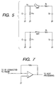
- the bit signal detecting section 106 has a current/voltage conversion circuit, like the one shown in Fig. 7, at the input portion.
- the tunnel current J T is converted into a voltage signal by this circuit, and the voltage signal is subjected to the subsequent processing.
- the detected bit signal is sent to a data extraction processing section 112.
- the signal is then reproduced as information.
- the bit signal is a signal obtained by amplifying the frequency component of the bit of the detected tunnel current.
- the data extraction processing section 112 reproduces the recorded information from the bit detection timing of the signal and the position information of the probe on the medium.
- the reproduced information is sent from the data extraction processing section 112 to an image data output section, an audio output section, or an information processing system for performing processing in accordance with the information, e.g., using the information as numerical data for a computer.
- the relative positional relationship between the recording medium 102 and the probe 101 can be changed by the scanning operation of a movable stage 104.
- the movable stage 104 incorporates an actuator, and moves the recording medium in directions (X and Y directions) within a plane of the recording medium surface in accordance with driving signals sent from a Y scan signal generating section 108 and an X scan signal generating section 109 through amplifiers 110.
- Each scan signal generating section (108, 109) generates a scan signal in accordance with a control signal output from a scan controlling section 107 on the basis of control information such as an offset position, a scan frequency, a main scan (X scan) width, and a sub-scan (Y scan) width.
- the scan controlling section 107 also sends the probe position information to the input device 111.
- the input device 111 then calculates the recording timing of a bit from the input value, and supplies a recording control signal to the bias applying section 105.
- Fig. 4 shows the inner arrangement of the bias applying section 105.
- the bias applying section 105 includes switches (SW1 and SW2), a charge storage capacitor C S having a capacitance C S , and a variable-output power supply V B (having an output V B ).
- the SW1 and the SW2 are ON/OFF-controlled by a switch timing control circuit 201 with reference to an input recording control signal.
- a bias is applied from the left output terminal of the SW1 to the medium.
- the bias applying section 105 also includes a line resistor or a limiting resistor R L for determining the leading edge of an applied pulse.
- steps 1 to 4 indicate control on the SW1 and the SW2 and the flow of charges.
- step 1 charges C S V B are stored in the charge storage capacitor C S .
- step 2 no electrical change occurs.
- the probe is scanned over the medium surface to be moved to a recording position.
- step 3 a pulse is actually applied.
- FIG. 5 shows an equivalent circuit of the pulse applying system.
- this circuit has a capacitance C T corresponding to the sum of the parasitic capacitances of the medium and other portions and medium resistors R T0 and R T1 .
- the charges C S V B are stored in the charge storage capacitor C S .
- Fig. 6 shows the behaviors of a current and a voltage.
- V M C S V B /(C S + C T ) According to this equation, V M can be increased by increasing V B .
- biases and pulses are applied to the medium.
- these biases and pulses can be applied from the probe side in the same manner as described above by only changing the output terminal of the circuit in Fig. 4 from the medium to the probe.
- a polyimide Langmuir-Blodgett (LB) film stacked on an Au electrode was used as a recording medium, and the bias applying circuit of the present invention was used to apply a bias voltage to the medium, thereby recording information thereon.
- the measured pulse applying time was about 50 ⁇ sec.
- the ON/OFF timings of the SW1 and the SW2 were set in the switch timing control circuit 201 in accordance with this measured time, and a pulse was applied.
- the voltage V B was set to a read voltage of 2.5 V, and a read operation was designated to the switch timing control circuit 201, thus closing both the SW1 and the SW2 and applying a DC bias to the medium.
- the charges stored in the charge storage means are output to the probe or a recording medium after the charge storage means is disconnected from the DC power supply.
- a bias and a current can be controlled in accordance with the local characteristics of the medium at the pulse applying position. This operation allows stable recording in terms of bit shape and position, and can greatly decrease the error rate in a recording/reproducing operation.
- the read error rate can be reduced without using any strong tracking mechanism.
- no redundant bits for error correction are required, and hence the system load in an encoding/decoding operation can be reduced.
- the recording density can be increased.
Landscapes
- Engineering & Computer Science (AREA)
- Chemical & Material Sciences (AREA)
- Nanotechnology (AREA)
- Physics & Mathematics (AREA)
- Mathematical Physics (AREA)
- Theoretical Computer Science (AREA)
- Crystallography & Structural Chemistry (AREA)
- Semiconductor Memories (AREA)
- Length Measuring Devices With Unspecified Measuring Means (AREA)
- Measuring Leads Or Probes (AREA)
- Measurement Of Length, Angles, Or The Like Using Electric Or Magnetic Means (AREA)
Applications Claiming Priority (3)
| Application Number | Priority Date | Filing Date | Title |
|---|---|---|---|
| JP28467096 | 1996-10-07 | ||
| JP28467096A JP3679525B2 (ja) | 1996-10-07 | 1996-10-07 | 情報記録再生装置、および情報記録再生方法 |
| JP284670/96 | 1996-10-07 |
Publications (2)
| Publication Number | Publication Date |
|---|---|
| EP0834875A2 true EP0834875A2 (de) | 1998-04-08 |
| EP0834875A3 EP0834875A3 (de) | 2001-03-28 |
Family
ID=17681470
Family Applications (1)
| Application Number | Title | Priority Date | Filing Date |
|---|---|---|---|
| EP97117269A Withdrawn EP0834875A3 (de) | 1996-10-07 | 1997-10-06 | Informationsaufzeichnungsgerät und -methode mittels Spannungsanlegung zwischen Sonde und Aufzeichnungsmedium |
Country Status (3)
| Country | Link |
|---|---|
| US (1) | US6040848A (de) |
| EP (1) | EP0834875A3 (de) |
| JP (1) | JP3679525B2 (de) |
Cited By (1)
| Publication number | Priority date | Publication date | Assignee | Title |
|---|---|---|---|---|
| US6040848A (en) * | 1996-10-07 | 2000-03-21 | Canon Kabushiki Kaisha | Information recording apparatus and method of recording information by applying voltage between probe and recording medium |
Families Citing this family (2)
| Publication number | Priority date | Publication date | Assignee | Title |
|---|---|---|---|---|
| KR100585462B1 (ko) * | 2003-12-26 | 2006-06-07 | 한국전자통신연구원 | 정보 저장 및 독출 장치 |
| KR100842890B1 (ko) | 2007-01-25 | 2008-07-03 | 삼성전자주식회사 | 탐침 또는 전도성 구조를 이용한 강유전층의 비트 기록 방법 |
Family Cites Families (25)
| Publication number | Priority date | Publication date | Assignee | Title |
|---|---|---|---|---|
| US3843846A (en) * | 1973-02-08 | 1974-10-22 | Rca Corp | Demountable capacitive protective coupling for pickup transducers |
| JPS5952571B2 (ja) * | 1979-10-04 | 1984-12-20 | 東北金属工業株式会社 | 方形波発生装置 |
| US4320491A (en) * | 1980-09-19 | 1982-03-16 | Rca Corporation | Apparatus for video disc stylus electrode reconditioning |
| JPS5922251A (ja) * | 1982-07-29 | 1984-02-04 | Toshiba Corp | 記録装置 |
| JPS59101049A (ja) * | 1982-11-30 | 1984-06-11 | Toshiba Corp | 記録再生装置 |
| JP2556491B2 (ja) * | 1986-12-24 | 1996-11-20 | キヤノン株式会社 | 記録装置及び記録法 |
| JP2556492B2 (ja) * | 1986-12-24 | 1996-11-20 | キヤノン株式会社 | 再生装置及び再生法 |
| US4896044A (en) * | 1989-02-17 | 1990-01-23 | Purdue Research Foundation | Scanning tunneling microscope nanoetching method |
| DE69030040T2 (de) * | 1989-09-07 | 1997-07-03 | Canon K.K., Tokio/Tokyo | Informationsspeicherung, -zugriff und -verarbeitung |
| JP2999282B2 (ja) * | 1990-03-09 | 2000-01-17 | キヤノン株式会社 | 記録再生方法及び装置 |
| JP2743213B2 (ja) * | 1990-07-25 | 1998-04-22 | キヤノン株式会社 | 記録及び/又は再生を行なう装置および方法 |
| JP2744359B2 (ja) * | 1991-04-24 | 1998-04-28 | キヤノン株式会社 | 情報再生及び/又は情報記録装置 |
| JP2930447B2 (ja) * | 1991-05-15 | 1999-08-03 | キヤノン株式会社 | 情報処理装置 |
| JP3029143B2 (ja) * | 1991-06-11 | 2000-04-04 | キヤノン株式会社 | 情報再生方法 |
| US5329122A (en) * | 1991-08-29 | 1994-07-12 | Canon Kabushiki Kaisha | Information processing apparatus and scanning tunnel microscope |
| JP3029499B2 (ja) * | 1992-05-07 | 2000-04-04 | キヤノン株式会社 | 記録再生装置 |
| US5323377A (en) * | 1992-11-27 | 1994-06-21 | Chen Zhi Q | Electrical data recording and retrieval based on impedance variation |
| EP0615235B9 (de) * | 1993-03-09 | 2003-11-12 | Canon Kabushiki Kaisha | Informationsaufzeichnungsmethode und -gerät |
| JPH0823014A (ja) * | 1994-07-08 | 1996-01-23 | Fujitsu Ltd | 信号波形測定装置及び信号波形測定方法 |
| JP3581475B2 (ja) * | 1995-02-13 | 2004-10-27 | キヤノン株式会社 | 情報処理装置 |
| JPH08297871A (ja) * | 1995-04-21 | 1996-11-12 | Hewlett Packard Co <Hp> | 高密度記録媒体及び大容量記録装置 |
| JP3576644B2 (ja) * | 1995-06-19 | 2004-10-13 | キヤノン株式会社 | 情報記録装置のプローブ及び記録媒体、並びにこれらを用いた情報記録方法 |
| JPH09120593A (ja) * | 1995-08-23 | 1997-05-06 | Sony Corp | 記録再生装置 |
| US5757760A (en) * | 1996-01-18 | 1998-05-26 | Canon Kabushiki Kaisha | Information recording and/or reproducing apparatus and method for performing recording and/or reproduction of information by using probe |
| JP3679525B2 (ja) * | 1996-10-07 | 2005-08-03 | キヤノン株式会社 | 情報記録再生装置、および情報記録再生方法 |
-
1996
- 1996-10-07 JP JP28467096A patent/JP3679525B2/ja not_active Expired - Fee Related
-
1997
- 1997-10-06 US US08/944,895 patent/US6040848A/en not_active Expired - Lifetime
- 1997-10-06 EP EP97117269A patent/EP0834875A3/de not_active Withdrawn
Cited By (1)
| Publication number | Priority date | Publication date | Assignee | Title |
|---|---|---|---|---|
| US6040848A (en) * | 1996-10-07 | 2000-03-21 | Canon Kabushiki Kaisha | Information recording apparatus and method of recording information by applying voltage between probe and recording medium |
Also Published As
| Publication number | Publication date |
|---|---|
| EP0834875A3 (de) | 2001-03-28 |
| JPH10112082A (ja) | 1998-04-28 |
| JP3679525B2 (ja) | 2005-08-03 |
| US6040848A (en) | 2000-03-21 |
Similar Documents
| Publication | Publication Date | Title |
|---|---|---|
| EP0529616B1 (de) | Informationsverarbeitungsgerät und Rastertunnelmikroskop | |
| JP3073616B2 (ja) | マルチプローブを具備する情報処理装置 | |
| JP3246987B2 (ja) | マルチプローブ制御回路を具備する情報処理装置 | |
| JPH06251435A (ja) | 記録再生装置 | |
| US5371728A (en) | Information recording/reproducing apparatus using probe | |
| US5371727A (en) | Scanning tunnel microscopy information processing system with noise detection to correct the tracking mechanism | |
| US5287342A (en) | Apparatus and method for reproducing information | |
| CA2080252C (en) | Information processing apparatus | |
| US6040848A (en) | Information recording apparatus and method of recording information by applying voltage between probe and recording medium | |
| US5535185A (en) | Information recording/reproduction apparatus using probe | |
| US5978326A (en) | Information processing apparatus using an offset signal to control the position of a probe | |
| US20050157575A1 (en) | Storage device and method | |
| US5517482A (en) | Information recording/reproducing apparatus having fuzzy operating unit | |
| JP3053142B2 (ja) | 情報処理装置 | |
| JP2983693B2 (ja) | 情報処理方法及び情報処理装置 | |
| JP3118654B2 (ja) | 情報処理装置及び走査型トンネル電子顕微鏡 | |
| JP3078141B2 (ja) | 記録装置および記録再生装置 | |
| JP3004823B2 (ja) | 情報処理装置 | |
| JP3039725B2 (ja) | 情報処理装置 | |
| JP3093946B2 (ja) | 記録媒体 | |
| JP4079397B2 (ja) | 記録再生装置のトラッキング機構及びトラッキング方法 | |
| JPH05109130A (ja) | 情報処理装置 | |
| JPH06119665A (ja) | 情報記録再生装置 | |
| JPH09282725A (ja) | 情報記録再生装置 | |
| JPH05314550A (ja) | 記録情報再生装置 |
Legal Events
| Date | Code | Title | Description |
|---|---|---|---|
| PUAI | Public reference made under article 153(3) epc to a published international application that has entered the european phase |
Free format text: ORIGINAL CODE: 0009012 |
|
| AK | Designated contracting states |
Kind code of ref document: A2 Designated state(s): DE FR GB IT |
|
| PUAL | Search report despatched |
Free format text: ORIGINAL CODE: 0009013 |
|
| AK | Designated contracting states |
Kind code of ref document: A3 Designated state(s): AT BE CH DE DK ES FI FR GB GR IE IT LI LU MC NL PT SE |
|
| 17P | Request for examination filed |
Effective date: 20010523 |
|
| AKX | Designation fees paid |
Free format text: DE FR GB IT |
|
| GRAH | Despatch of communication of intention to grant a patent |
Free format text: ORIGINAL CODE: EPIDOS IGRA |
|
| STAA | Information on the status of an ep patent application or granted ep patent |
Free format text: STATUS: THE APPLICATION IS DEEMED TO BE WITHDRAWN |
|
| 18D | Application deemed to be withdrawn |
Effective date: 20030422 |