EP0834927A2 - Halbleiter-IC-Anordnung - Google Patents
Halbleiter-IC-Anordnung Download PDFInfo
- Publication number
- EP0834927A2 EP0834927A2 EP97300960A EP97300960A EP0834927A2 EP 0834927 A2 EP0834927 A2 EP 0834927A2 EP 97300960 A EP97300960 A EP 97300960A EP 97300960 A EP97300960 A EP 97300960A EP 0834927 A2 EP0834927 A2 EP 0834927A2
- Authority
- EP
- European Patent Office
- Prior art keywords
- semiconductor
- pad
- semiconductor chip
- well portion
- function region
- Prior art date
- Legal status (The legal status is an assumption and is not a legal conclusion. Google has not performed a legal analysis and makes no representation as to the accuracy of the status listed.)
- Withdrawn
Links
Images


Classifications
-
- H—ELECTRICITY
- H10—SEMICONDUCTOR DEVICES; ELECTRIC SOLID-STATE DEVICES NOT OTHERWISE PROVIDED FOR
- H10D—INORGANIC ELECTRIC SEMICONDUCTOR DEVICES
- H10D30/00—Field-effect transistors [FET]
- H10D30/60—Insulated-gate field-effect transistors [IGFET]
- H10D30/64—Double-diffused metal-oxide semiconductor [DMOS] FETs
- H10D30/66—Vertical DMOS [VDMOS] FETs
-
- H—ELECTRICITY
- H10—SEMICONDUCTOR DEVICES; ELECTRIC SOLID-STATE DEVICES NOT OTHERWISE PROVIDED FOR
- H10D—INORGANIC ELECTRIC SEMICONDUCTOR DEVICES
- H10D10/00—Bipolar junction transistors [BJT]
- H10D10/40—Vertical BJTs
- H10D10/421—Vertical BJTs having both emitter-base and base-collector junctions ending at the same surface of the body
-
- H—ELECTRICITY
- H10—SEMICONDUCTOR DEVICES; ELECTRIC SOLID-STATE DEVICES NOT OTHERWISE PROVIDED FOR
- H10D—INORGANIC ELECTRIC SEMICONDUCTOR DEVICES
- H10D10/00—Bipolar junction transistors [BJT]
- H10D10/60—Lateral BJTs
-
- H—ELECTRICITY
- H10—SEMICONDUCTOR DEVICES; ELECTRIC SOLID-STATE DEVICES NOT OTHERWISE PROVIDED FOR
- H10D—INORGANIC ELECTRIC SEMICONDUCTOR DEVICES
- H10D64/00—Electrodes of devices having potential barriers
- H10D64/20—Electrodes characterised by their shapes, relative sizes or dispositions
- H10D64/23—Electrodes carrying the current to be rectified, amplified, oscillated or switched, e.g. sources, drains, anodes or cathodes
- H10D64/251—Source or drain electrodes for field-effect devices
- H10D64/252—Source or drain electrodes for field-effect devices for vertical or pseudo-vertical devices
-
- H—ELECTRICITY
- H10—SEMICONDUCTOR DEVICES; ELECTRIC SOLID-STATE DEVICES NOT OTHERWISE PROVIDED FOR
- H10D—INORGANIC ELECTRIC SEMICONDUCTOR DEVICES
- H10D64/00—Electrodes of devices having potential barriers
- H10D64/20—Electrodes characterised by their shapes, relative sizes or dispositions
- H10D64/27—Electrodes not carrying the current to be rectified, amplified, oscillated or switched, e.g. gates
- H10D64/311—Gate electrodes for field-effect devices
- H10D64/411—Gate electrodes for field-effect devices for FETs
- H10D64/511—Gate electrodes for field-effect devices for FETs for IGFETs
- H10D64/517—Gate electrodes for field-effect devices for FETs for IGFETs characterised by the conducting layers
- H10D64/519—Gate electrodes for field-effect devices for FETs for IGFETs characterised by the conducting layers characterised by their top-view geometrical layouts
-
- H—ELECTRICITY
- H10—SEMICONDUCTOR DEVICES; ELECTRIC SOLID-STATE DEVICES NOT OTHERWISE PROVIDED FOR
- H10W—GENERIC PACKAGES, INTERCONNECTIONS, CONNECTORS OR OTHER CONSTRUCTIONAL DETAILS OF DEVICES COVERED BY CLASS H10
- H10W72/00—Interconnections or connectors in packages
- H10W72/90—Bond pads, in general
-
- H—ELECTRICITY
- H10—SEMICONDUCTOR DEVICES; ELECTRIC SOLID-STATE DEVICES NOT OTHERWISE PROVIDED FOR
- H10D—INORGANIC ELECTRIC SEMICONDUCTOR DEVICES
- H10D62/00—Semiconductor bodies, or regions thereof, of devices having potential barriers
- H10D62/10—Shapes, relative sizes or dispositions of the regions of the semiconductor bodies; Shapes of the semiconductor bodies
- H10D62/102—Constructional design considerations for preventing surface leakage or controlling electric field concentration
- H10D62/103—Constructional design considerations for preventing surface leakage or controlling electric field concentration for increasing or controlling the breakdown voltage of reverse-biased devices
- H10D62/105—Constructional design considerations for preventing surface leakage or controlling electric field concentration for increasing or controlling the breakdown voltage of reverse-biased devices by having particular doping profiles, shapes or arrangements of PN junctions; by having supplementary regions, e.g. junction termination extension [JTE]
- H10D62/106—Constructional design considerations for preventing surface leakage or controlling electric field concentration for increasing or controlling the breakdown voltage of reverse-biased devices by having particular doping profiles, shapes or arrangements of PN junctions; by having supplementary regions, e.g. junction termination extension [JTE] having supplementary regions doped oppositely to or in rectifying contact with regions of the semiconductor bodies, e.g. guard rings with PN or Schottky junctions
-
- H—ELECTRICITY
- H10—SEMICONDUCTOR DEVICES; ELECTRIC SOLID-STATE DEVICES NOT OTHERWISE PROVIDED FOR
- H10D—INORGANIC ELECTRIC SEMICONDUCTOR DEVICES
- H10D62/00—Semiconductor bodies, or regions thereof, of devices having potential barriers
- H10D62/10—Shapes, relative sizes or dispositions of the regions of the semiconductor bodies; Shapes of the semiconductor bodies
- H10D62/124—Shapes, relative sizes or dispositions of the regions of semiconductor bodies or of junctions between the regions
- H10D62/126—Top-view geometrical layouts of the regions or the junctions
- H10D62/127—Top-view geometrical layouts of the regions or the junctions of cellular field-effect devices, e.g. multicellular DMOS transistors or IGBTs
-
- H—ELECTRICITY
- H10—SEMICONDUCTOR DEVICES; ELECTRIC SOLID-STATE DEVICES NOT OTHERWISE PROVIDED FOR
- H10D—INORGANIC ELECTRIC SEMICONDUCTOR DEVICES
- H10D64/00—Electrodes of devices having potential barriers
- H10D64/20—Electrodes characterised by their shapes, relative sizes or dispositions
- H10D64/27—Electrodes not carrying the current to be rectified, amplified, oscillated or switched, e.g. gates
- H10D64/311—Gate electrodes for field-effect devices
- H10D64/411—Gate electrodes for field-effect devices for FETs
- H10D64/511—Gate electrodes for field-effect devices for FETs for IGFETs
-
- H—ELECTRICITY
- H10—SEMICONDUCTOR DEVICES; ELECTRIC SOLID-STATE DEVICES NOT OTHERWISE PROVIDED FOR
- H10W—GENERIC PACKAGES, INTERCONNECTIONS, CONNECTORS OR OTHER CONSTRUCTIONAL DETAILS OF DEVICES COVERED BY CLASS H10
- H10W72/00—Interconnections or connectors in packages
- H10W72/50—Bond wires
- H10W72/531—Shapes of wire connectors
- H10W72/536—Shapes of wire connectors the connected ends being ball-shaped
-
- H—ELECTRICITY
- H10—SEMICONDUCTOR DEVICES; ELECTRIC SOLID-STATE DEVICES NOT OTHERWISE PROVIDED FOR
- H10W—GENERIC PACKAGES, INTERCONNECTIONS, CONNECTORS OR OTHER CONSTRUCTIONAL DETAILS OF DEVICES COVERED BY CLASS H10
- H10W72/00—Interconnections or connectors in packages
- H10W72/50—Bond wires
- H10W72/59—Bond pads specially adapted therefor
-
- H—ELECTRICITY
- H10—SEMICONDUCTOR DEVICES; ELECTRIC SOLID-STATE DEVICES NOT OTHERWISE PROVIDED FOR
- H10W—GENERIC PACKAGES, INTERCONNECTIONS, CONNECTORS OR OTHER CONSTRUCTIONAL DETAILS OF DEVICES COVERED BY CLASS H10
- H10W72/00—Interconnections or connectors in packages
- H10W72/90—Bond pads, in general
- H10W72/931—Shapes of bond pads
- H10W72/932—Plan-view shape, i.e. in top view
-
- H—ELECTRICITY
- H10—SEMICONDUCTOR DEVICES; ELECTRIC SOLID-STATE DEVICES NOT OTHERWISE PROVIDED FOR
- H10W—GENERIC PACKAGES, INTERCONNECTIONS, CONNECTORS OR OTHER CONSTRUCTIONAL DETAILS OF DEVICES COVERED BY CLASS H10
- H10W72/00—Interconnections or connectors in packages
- H10W72/90—Bond pads, in general
- H10W72/931—Shapes of bond pads
- H10W72/934—Cross-sectional shape, i.e. in side view
-
- H—ELECTRICITY
- H10—SEMICONDUCTOR DEVICES; ELECTRIC SOLID-STATE DEVICES NOT OTHERWISE PROVIDED FOR
- H10W—GENERIC PACKAGES, INTERCONNECTIONS, CONNECTORS OR OTHER CONSTRUCTIONAL DETAILS OF DEVICES COVERED BY CLASS H10
- H10W72/00—Interconnections or connectors in packages
- H10W72/90—Bond pads, in general
- H10W72/951—Materials of bond pads
-
- H—ELECTRICITY
- H10—SEMICONDUCTOR DEVICES; ELECTRIC SOLID-STATE DEVICES NOT OTHERWISE PROVIDED FOR
- H10W—GENERIC PACKAGES, INTERCONNECTIONS, CONNECTORS OR OTHER CONSTRUCTIONAL DETAILS OF DEVICES COVERED BY CLASS H10
- H10W72/00—Interconnections or connectors in packages
- H10W72/90—Bond pads, in general
- H10W72/981—Auxiliary members, e.g. spacers
- H10W72/983—Reinforcing structures, e.g. collars
Definitions
- the present invention relates to a semiconductor IC device, and more particularly to a semiconductor IC device with a high dielectric strength as in the insulated gate FET (IGFET).
- IGFET insulated gate FET
- a MOS FET metal-oxide-semiconductor field effect transistor
- MOS capacitor formed by a silicon substrate and a gate arranged on the silicon substrate through the intermediary of a gate oxide film, and a source for supply of carriers and a drain for taking out the carriers.
- Figures 5 and 6 are a plan view and a cross sectional view respectively showing the basic structure of a conventional semiconductor IC device called a VDMOS FET (vertical double-diffused MOS FET).
- VDMOS FET vertical double-diffused MOS FET
- a dual well structure which includes a first well portion 3 (see Figure 6) in the silicon substrate and a second well portion 4 (see Figure 6) in the first well portion 3, these wells being successively formed by double diffusion of impurities into the silicon substrate 2. If a dual well structure is expressed as a cell 5, a plurality of cells 5 are arranged in the center of the silicon substrate 2.
- a pair of pads 6 and 7 are provided, and the surface of the silicon substrate 2 is protected by a passivation film 8 which leaves the pads 6 and 7 exposed, and a peripheral area of the silicon substrate 2 also exposed.
- a gate is arranged on each of the first well portions 3 through the intermediary of a gate oxide film, not shown.
- a source is formed in each of the second well portions 4.
- a drain electrode 9 for the drain, composed of the body of the silicon substrate 2, is formed on the reverse side of the silicon substrate 2.
- the gates of the cells 5 are collectively connected to one pad 6, while the sources, that is, the second well portions 4 are collectively connected to the other pad 7.
- the depletion layer 10 to increase the dielectric strength between the drain and the source is formed in such a way as to surround all well structures, that is, the cells 5 in the silicon substrate 2.
- a field plate 11, which serves to improve the dielectric strength by expanding the depletion layer 10 is disposed between the surface of the silicon substrate 2 and the passivation layer 8.
- Bonding wires 12 extend from the pads 6 and 7 to external terminals, not shown.
- VDMOS 1 on account of the presence of the depletion layer 10, even if a voltage of 1000 V, for example, is applied between the drain and the source, a direct dielectric breakdown between drain and source is certainly prevented so long as a gate voltage is not applied to the gate.
- the pads 6 and 7 are arranged so close to the peripheral edge of the silicon substrate 2 as to be adjacent to the field plate 11 to shorten the length of the bonding wires 12 for reasons of installation of the bonding wires 12 led outward from the silicon substrate 2.
- Figures 7 and 8 are respectively a plan view and a cross sectional view showing the basic structure of a conventional semiconductor IC device called a high voltage IC bipolar transistor (dielectric strength : about 1000 V).
- a dual well structure is adopted for this bipolar transistor 20, which basically includes a first well portion 23 (see Figure 8) in the silicon substrate and a second well portion 24 (see Figure 8) in the first well portion, successively formed by double diffusion of impurities into the silicon substrate 22 as in the VDMOS 1 shown in Figures 5 and 6. If each dual well structure is called a cell 25, a plurality of cells 25 are arranged in the center of the silicon substrate 22.
- a base is formed in each first well portion 23, and an emitter is formed in each second well portion 24.
- a collector electrode 29 for the collector region, composed of the body of the silicon substrate 22, is formed on the reverse side of the silicon substrate 22.
- the bases of the cells 25 are collectively connected to one pad 26 as the combined base, and the emitters of the cells 25 are collectively connected to the other pad 27 as the combined emitter.
- a depletion layer 30 to increase the dielectric strength between the collector and the base is so formed as to surround all cells 25 in the silicon substrate 22 as in the example shown in Figure 6.
- a field plate 31, which serves to improve the dielectric strength, is arranged between the surface of the silicon substrate 22 and the passivation film 28.
- this transistor 20 owing to the presence of the depletion layer 30, even if a voltage of 1000 V, for example, is applied between the base and the collector, a direct dielectric breakdown is certainly prevented so long as a current does not flow between base and emitter.
- the pads 26 and 27 are arranged so close to the peripheral edge of the silicon substrate 22 as to be adjacent to the field plate 31 to shorten the length of the bonding wires 32 for reasons of installation of the bonding wires 32 led outward from the silicon substrate 22, the space between the pads 26 and 27, and the grid line 33 of the silicon substrate 22 extending beyond the peripheral edge of the passivation film 28 becomes relatively small.
- an object of the present invention is to provide a semiconductor IC device which does not incur a decrease in the dielectric strength by a leakage current flowing over the surface of the semiconductor device.
- a semiconductor IC device comprising a semiconductor chip including at least a first function region, a second function region, and a third function region, wherein a current flowing through the third function region is controlled by an electric signal input to the first function region; and a first and a second pad provided on a surface of the semiconductor chip and serving as electric connectors for the first and second function regions, wherein in the semiconductor chip, when there is no electric signal input to the first function region, a depletion layer is so formed as to surround the first and second function regions between the first and second function regions, and the third function region, and wherein in order to improve the dielectric strength between the first and second function regions, and the third function region, the first and second pads are arranged close to each other substantially in the center of the surface of the semiconductor chip.
- the space between the peripheral edge of the semiconductor chip, and the first and second pad can be made larger than before.
- dielectric breakdown by a surface leakage current can be prevented securely.
- the present invention can be applied to MOS FETs and bipolar transistors.
- a dual well structure is preferably adopted in which the first function portion is formed by a first well portion and a second well portion is nested in the first well portion.
- a plurality of cells, each of this dual well structure, may be so arranged as to surround the first and second pads.
- the portion whereby to improve the dielectric strength is preferably formed of a field plate structure to manufacture a semiconductor IC device in a compact form.
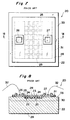
- Figures 1 and 2 show examples in which the present invention is applied to a high-power high-dielectric strength VDMOS like the one shown in Figures 5 and 6, and in Figures 1 and 2, the elements identical with those in Figures 5 and 6 are designated by the same reference numerals.
- the VDMOS FET 50 comprises a semiconductor chip 51, and a pair of pads 52 and 53 formed on the semiconductor chip 51.
- the semiconductor chip 51 is obtained by growing an n - -type silicon epitaxial layer 55 on an n-type silicon crystal substrate, for example.
- a plurality of cells 58 are provided which are of a dual well structure including a first well portion 56 (see Figure 2) and a second well portion 57 (see Figure 2) in the first well portion 56, successively formed by double diffusion of impurities into the substrate 51 as is conventionally done.
- the first well portion 56 has a polarity (p) opposite from that of the substrate 51.
- its central part 57a shows the same polarity as the first well portion 56, and the two side parts 57b show a polarity (n) opposite from that of the first well portion 56.
- the first well portion 56 serves as the first function region, and has a gate 60 deposited on its top surface through the intermediary of a gate oxide film 59.
- a voltage as an electric signal is applied to the gate 60, in the first well portion 56, a channel is formed to electrically connect the second well portion 57 to the drain region 51 composed of the body of the substrate 51 which serves as the third function region as is conventionally done.
- the gates 60 of the respective cells 58 are collectively connected to the pad 52 through a conductive means, not shown, which has conventionally been used and is here omitted for simplicity of the drawing.
- the second well portion 57 serves as the second function region. Being in contact on its side parts 57b with the first well portion 56, the second function region is electrically connected through the channel to the substrate 51, which is the drain region, and therefore functions as the source region.
- the central part 57a serves to increase the dielectric strength between the source and the drain, and by connecting to the first well portion 56, prevent an electric stray in the first well portion 56.
- the second well portions 57 that is, the source regions 57 are collectively connected to the pad 53 through a conductive means, not shown, which is conventionally used.
- the pads 52 and 53 having the gates 60 and the sources 57 of a plurality of cells 58 collectively connected thereto are arranged close to each other substantially in the center of that surface 51a of the substrate 51 where the cells 58 are provided.
- Those cells 58 are arranged in such a manner as to surround this pair of pads 52 and 53.
- a drain electrode 9 is provided, while on the top surface of the substrate 51, a bonding wire 12, same as the one conventionally used, extends from each of the pads 52 and 53.
- the depletion layer 10 to secure the dielectric strength between drain and source is formed between the cells 58 and the drain in such a manner as to surround all cells 58 in the substrate 51.
- the p-well portions 61 are provided under the pads 52 and 53 to expand the depletion layer 10 to thereby increase the dielectric strength of the device.
- a conventional passivation film 62 is deposited which leaves the grid line 13 as well as the pads 52 and 53 exposed. Moreover, in order to improve the dielectric strength, a conventional field plate 11 is arranged along and beneath the peripheral area of the passivation film 62 and above the surface 51a of the substrate 51.
- a guard ring structure may be adopted, but a field plate 11 is to be preferably adopted to make a VDMOS FET 50 in a compact size.
- the source and gate are grounded, and a voltage of 1000 V is applied to the drain.
- a voltage of 1000 V is applied to the drain.
- a predetermined voltage higher than 1000 V as mentioned above, for example is applied between the drain and the source, while no voltage is applied to the gate pad 52, a leakage current does not occur between drain and source in the substrate 51, so that a decrease in the dielectric strength by a leakage current does not occur, which used to occur in the past.
- a pair of the pads 52 and 53 are arranged in the center of the surface 51a of the substrate 51 remote from the grid line 13 which is the exposed area at the periphery of the substrate 51. Therefore, the occurrence of a leakage current as in the past can be certainly prevented, which flows over the surface of the passivation film 62 between the grid line 13 and the pad 52 or between the grid line 13 and the pad 53.
- the decrease in the dielectric strength due to a leakage current between the drain and the source or between drain and gate over the surface of the semiconductor IC device 50 can be certainly prevented, thus improving the dielectric strength of the device.
- Figures 3 and 4 show an example in which the present invention is applied to a high-dielectric-strength bipolar transistor similar to the one shown in Figures 7 and 8.
- the elements identical with those in Figures 7 and 8 are designated by the same reference numerals.
- a high-dielectric-strength bipolar transistor 70 comprises a semiconductor chip 71, and a pair of pads 72 and 73 formed on the semiconductor chip 71 as shown in Figures 3 and 4.
- the semiconductor chip is obtained by growing an n - -type silicon epitaxial layer 75 on an n-type silicon crystal substrate 74, for example.
- a plurality of cells 78 are provided which are of a dual well structure including a first well portion 76 (see Figure 4) and a second well portion 77 (see Figure 4) in the first well portion, successively formed by double diffusion of impurities into the substrate 71 as is conventionally done.
- the first well portion 76 has a polarity (p) opposite from that of the substrate 71.
- the second well portion 77 shows a polarity (n) opposite from that of the first well portion 76.
- the first well portion 76 which is the first function region, serves as a base.
- the second well portion 77 which is the second function region, serves as an emitter.
- the third function region composed of the body of the substrate 71 serves as a collector, and on the reverse side of the substrate 71, a collector electrode 29 is formed.
- the bases 76 of the respective cells 78 are collectively connected to the pad 72 through a conductive means, not shown, which has conventionally been used and is here omitted for simplicity of the drawing.
- the emitters of the respective cells 78 are collectively connected to the pad 73 through a conductive means, not shown, which has conventionally been used.
- the pads 72 and 73 having the bases 76 and the emitters 77 of a plurality of cells 78 collectively connected thereto are arranged close to each other substantially in the center of that surface 71a of the substrate 71 where the cells 78 are provided.
- Those cells 78 are arranged in such a manner as to surround this pair of pads 72 and 73.
- a bonding wire 32 same as the one conventionally used extends from each of the pads 72 and 73.
- each transistor 70 of the p-n-p type has its base grounded, for example, and a current does not flow from base to emitter, a depletion layer 30 to ensure the collector-base dielectric strength is formed between the cells and the collector in such a way as to surround all cells 78 in the substrate 71.
- the p-well portions are provided under the pads 72 and 73 to expand the depletion layer 30 to thereby increase the dielectric strength of the device.
- a conventional passivation film 80 is deposited which leaves the grid line 33 as well as the pads 72 and 73 exposed. Moreover, in order to improve the dielectric strength, a conventional field plate 31 is arranged along and beneath the peripheral area of the passivation film 80 and above the surface 71a of the substrate 71.
- the collector current can be controlled.
- the depletion layer 30 to secure the dielectric strength exists. Therefore, even when a predetermined voltage in excess of 1000 V, for example, is applied between the collector and the emitter, a leakage current does not occur between collector and emitter in the substrate 71, so that a decrease in the dielectric strength by a leakage current does not come to pass, which used to be a problem in the past.
- a pair of the pads 72 and 73 are arranged in the center of the surface 71a of the substrate 71 remote from the grid line 33 which is the exposed area at the periphery of the substrate 71. Therefore, the occurrence of a leakage current as in the past can be certainly prevented, which flows over the surface of the passivation film 80 between the grid line 33 and the base pad 72 or between the grid line 33 and the emitter pad 73.
- the decrease in the dielectric strength due to a collector-base leakage current between the base pad 72 and the grid line 33 or between the emitter pad 73 and the grid line 33 over the surface of the semiconductor IC device 70 can be certainly prevented, thus improving the dielectric strength of the device.
- the present invention is applied to a high-dielectric-strength VDMOS FET and a high-dielectric-strength bipolar transistor as a semiconductor IC device with a high dielectric strength.
- the present invention is not limited to those examples, but can be applied to other various types of high-dielectric-strength semiconductor IC devices , such as an insulated gate FET (IGFET), and a lateral double-diffused MOS FET (LDMOS) in which the drain electrode is provided on the top surface of an IC chip where the source pad and the drain pad are formed.
- IGFET insulated gate FET
- LDMOS lateral double-diffused MOS FET
- the manufacturing process of the semiconductor IC device, the polarity and material of the semiconductor chip, the number of pads, the connection arrangement of the respective function regions, the applied voltages, etc. in the embodiments described above can be selected as you think suitable.
Landscapes
- Semiconductor Integrated Circuits (AREA)
- Metal-Oxide And Bipolar Metal-Oxide Semiconductor Integrated Circuits (AREA)
- Bipolar Transistors (AREA)
- Wire Bonding (AREA)
Applications Claiming Priority (2)
| Application Number | Priority Date | Filing Date | Title |
|---|---|---|---|
| JP8261781A JPH10107061A (ja) | 1996-10-02 | 1996-10-02 | 半導体集積回路装置 |
| JP261781/96 | 1996-10-02 |
Publications (2)
| Publication Number | Publication Date |
|---|---|
| EP0834927A2 true EP0834927A2 (de) | 1998-04-08 |
| EP0834927A3 EP0834927A3 (de) | 1998-09-09 |
Family
ID=17366620
Family Applications (1)
| Application Number | Title | Priority Date | Filing Date |
|---|---|---|---|
| EP97300960A Withdrawn EP0834927A3 (de) | 1996-10-02 | 1997-02-14 | Halbleiter-IC-Anordnung |
Country Status (4)
| Country | Link |
|---|---|
| US (1) | US5814860A (de) |
| EP (1) | EP0834927A3 (de) |
| JP (1) | JPH10107061A (de) |
| KR (1) | KR100312467B1 (de) |
Families Citing this family (6)
| Publication number | Priority date | Publication date | Assignee | Title |
|---|---|---|---|---|
| TWI220565B (en) * | 2003-02-26 | 2004-08-21 | Realtek Semiconductor Corp | Structure of IC bond pad and its formation method |
| KR100648276B1 (ko) * | 2004-12-15 | 2006-11-23 | 삼성전자주식회사 | 역방향 다이오드가 구비된 수직형 디모스 소자 |
| US9647077B2 (en) * | 2013-12-23 | 2017-05-09 | Jsab Technologies Limited | Power semiconductor devices having a semi-insulating field plate |
| JP6319028B2 (ja) | 2014-10-03 | 2018-05-09 | 三菱電機株式会社 | 半導体装置 |
| US11393692B2 (en) * | 2017-08-17 | 2022-07-19 | Semiconductor Components Industries, Llc | Semiconductor package electrical contact structures and related methods |
| TR201806277A2 (tr) | 2018-05-03 | 2018-05-21 | Deniz Kusaslan | Pencere çocuk güvenli̇k si̇stemi̇ |
Family Cites Families (4)
| Publication number | Priority date | Publication date | Assignee | Title |
|---|---|---|---|---|
| JPS5987828A (ja) * | 1982-11-12 | 1984-05-21 | Hitachi Ltd | 半導体装置 |
| JPS60133745A (ja) * | 1983-12-21 | 1985-07-16 | Fujitsu Ltd | 高耐圧トランジスタ |
| JP3150443B2 (ja) * | 1992-09-10 | 2001-03-26 | 株式会社東芝 | 半導体装置 |
| DE69321966T2 (de) * | 1993-12-24 | 1999-06-02 | Consorzio Per La Ricerca Sulla Microelettronica Nel Mezzogiorno, Catania | Leistungs-Halbleiterbauelement |
-
1996
- 1996-10-02 JP JP8261781A patent/JPH10107061A/ja not_active Withdrawn
-
1997
- 1997-02-14 EP EP97300960A patent/EP0834927A3/de not_active Withdrawn
- 1997-02-24 US US08/804,828 patent/US5814860A/en not_active Expired - Lifetime
- 1997-05-22 KR KR1019970019990A patent/KR100312467B1/ko not_active Expired - Fee Related
Also Published As
| Publication number | Publication date |
|---|---|
| KR100312467B1 (ko) | 2002-01-12 |
| KR19980032131A (ko) | 1998-07-25 |
| US5814860A (en) | 1998-09-29 |
| JPH10107061A (ja) | 1998-04-24 |
| EP0834927A3 (de) | 1998-09-09 |
Similar Documents
| Publication | Publication Date | Title |
|---|---|---|
| JP3214818B2 (ja) | レベルシフト操作を有し、金属クロスオーバを有しない高電圧電力用集積回路 | |
| US5589405A (en) | Method for fabricating VDMOS transistor with improved breakdown characteristics | |
| US5282018A (en) | Power semiconductor device having gate structure in trench | |
| US4789882A (en) | High power MOSFET with direct connection from connection pads to underlying silicon | |
| US6552597B1 (en) | Integrated circuit with closely coupled high voltage output and offline transistor pair | |
| US5557127A (en) | Termination structure for mosgated device with reduced mask count and process for its manufacture | |
| US5633525A (en) | Lateral field effect transistor | |
| JPS61182264A (ja) | 縦型mosトランジスタ | |
| JPH05503190A (ja) | パワーmosfetトランジスタ回路 | |
| EP0494597A1 (de) | Leistungshalbleiteranordnung mit einer Graben-Gateelektrode | |
| JP2877408B2 (ja) | 導電変調型mosfet | |
| US20010040266A1 (en) | Integrated circuit with highly efficient junction insulation | |
| JP2954854B2 (ja) | 集積回路チップ | |
| US5814860A (en) | Semiconductor IC device having first and second pads on surface of semiconductor chip | |
| US5874767A (en) | Semiconductor device including a lateral power device | |
| JPS63311766A (ja) | Misパワートランジスタ | |
| JP2996722B2 (ja) | 一体型esd保護を備えたnmos素子 | |
| JPH07142731A (ja) | パワーデバイスおよびそれを形成するための方法 | |
| US20100102379A1 (en) | Lateral diffused metal oxide semiconductor device | |
| US6043534A (en) | High voltage semiconductor device | |
| US5317182A (en) | Termination of the power stage of a monolithic semiconductor device | |
| JP3349029B2 (ja) | 半導体装置 | |
| JP2797688B2 (ja) | 伝導度変調型misfetを備えた半導体装置 | |
| JPS5987828A (ja) | 半導体装置 | |
| US20020167044A1 (en) | Semiconductor component with an edge termination that is suitable for high voltage |
Legal Events
| Date | Code | Title | Description |
|---|---|---|---|
| PUAI | Public reference made under article 153(3) epc to a published international application that has entered the european phase |
Free format text: ORIGINAL CODE: 0009012 |
|
| AK | Designated contracting states |
Kind code of ref document: A2 Designated state(s): AT DE GB |
|
| AX | Request for extension of the european patent |
Free format text: AL;LT;LV;RO;SI |
|
| PUAL | Search report despatched |
Free format text: ORIGINAL CODE: 0009013 |
|
| AK | Designated contracting states |
Kind code of ref document: A3 Designated state(s): AT BE CH DE DK ES FI FR GB GR IE IT LI LU MC NL PT SE |
|
| AX | Request for extension of the european patent |
Free format text: AL;LT;LV;RO;SI |
|
| 17P | Request for examination filed |
Effective date: 19990210 |
|
| AKX | Designation fees paid |
Free format text: AT DE GB |
|
| RBV | Designated contracting states (corrected) |
Designated state(s): AT DE GB |
|
| STAA | Information on the status of an ep patent application or granted ep patent |
Free format text: STATUS: THE APPLICATION IS DEEMED TO BE WITHDRAWN |
|
| 18D | Application deemed to be withdrawn |
Effective date: 20060620 |