EP0835049A2 - Appareil et méthode pour réaliser un chemin conducteur résistant à la corrosion à travers des joints ou des interstices non conducteurs - Google Patents
Appareil et méthode pour réaliser un chemin conducteur résistant à la corrosion à travers des joints ou des interstices non conducteurs Download PDFInfo
- Publication number
- EP0835049A2 EP0835049A2 EP97202940A EP97202940A EP0835049A2 EP 0835049 A2 EP0835049 A2 EP 0835049A2 EP 97202940 A EP97202940 A EP 97202940A EP 97202940 A EP97202940 A EP 97202940A EP 0835049 A2 EP0835049 A2 EP 0835049A2
- Authority
- EP
- European Patent Office
- Prior art keywords
- conductive
- bridge
- mesh
- peaks
- intersection
- Prior art date
- Legal status (The legal status is an assumption and is not a legal conclusion. Google has not performed a legal analysis and makes no representation as to the accuracy of the status listed.)
- Withdrawn
Links
Images


Classifications
-
- B—PERFORMING OPERATIONS; TRANSPORTING
- B32—LAYERED PRODUCTS
- B32B—LAYERED PRODUCTS, i.e. PRODUCTS BUILT-UP OF STRATA OF FLAT OR NON-FLAT, e.g. CELLULAR OR HONEYCOMB, FORM
- B32B3/00—Layered products comprising a layer with external or internal discontinuities or unevennesses, or a layer of non-planar shape; Layered products comprising a layer having particular features of form
- B32B3/02—Layered products comprising a layer with external or internal discontinuities or unevennesses, or a layer of non-planar shape; Layered products comprising a layer having particular features of form characterised by features of form at particular places, e.g. in edge regions
- B32B3/08—Layered products comprising a layer with external or internal discontinuities or unevennesses, or a layer of non-planar shape; Layered products comprising a layer having particular features of form characterised by features of form at particular places, e.g. in edge regions characterised by added members at particular parts
-
- B—PERFORMING OPERATIONS; TRANSPORTING
- B32—LAYERED PRODUCTS
- B32B—LAYERED PRODUCTS, i.e. PRODUCTS BUILT-UP OF STRATA OF FLAT OR NON-FLAT, e.g. CELLULAR OR HONEYCOMB, FORM
- B32B3/00—Layered products comprising a layer with external or internal discontinuities or unevennesses, or a layer of non-planar shape; Layered products comprising a layer having particular features of form
- B32B3/26—Layered products comprising a layer with external or internal discontinuities or unevennesses, or a layer of non-planar shape; Layered products comprising a layer having particular features of form characterised by a particular shape of the outline of the cross-section of a continuous layer; characterised by a layer with cavities or internal voids ; characterised by an apertured layer
- B32B3/266—Layered products comprising a layer with external or internal discontinuities or unevennesses, or a layer of non-planar shape; Layered products comprising a layer having particular features of form characterised by a particular shape of the outline of the cross-section of a continuous layer; characterised by a layer with cavities or internal voids ; characterised by an apertured layer characterised by an apertured layer, the apertures going through the whole thickness of the layer, e.g. expanded metal, perforated layer, slit layer regular cells B32B3/12
-
- B—PERFORMING OPERATIONS; TRANSPORTING
- B32—LAYERED PRODUCTS
- B32B—LAYERED PRODUCTS, i.e. PRODUCTS BUILT-UP OF STRATA OF FLAT OR NON-FLAT, e.g. CELLULAR OR HONEYCOMB, FORM
- B32B15/00—Layered products comprising a layer of metal
- B32B15/14—Layered products comprising a layer of metal next to a fibrous or filamentary layer
-
- B—PERFORMING OPERATIONS; TRANSPORTING
- B64—AIRCRAFT; AVIATION; COSMONAUTICS
- B64D—EQUIPMENT FOR FITTING IN OR TO AIRCRAFT; FLIGHT SUITS; PARACHUTES; ARRANGEMENT OR MOUNTING OF POWER PLANTS OR PROPULSION TRANSMISSIONS IN AIRCRAFT
- B64D45/00—Aircraft indicators or protectors not otherwise provided for
- B64D45/02—Lightning protectors; Static dischargers
-
- B—PERFORMING OPERATIONS; TRANSPORTING
- B32—LAYERED PRODUCTS
- B32B—LAYERED PRODUCTS, i.e. PRODUCTS BUILT-UP OF STRATA OF FLAT OR NON-FLAT, e.g. CELLULAR OR HONEYCOMB, FORM
- B32B2305/00—Condition, form or state of the layers or laminate
- B32B2305/38—Meshes, lattices or nets
-
- B—PERFORMING OPERATIONS; TRANSPORTING
- B32—LAYERED PRODUCTS
- B32B—LAYERED PRODUCTS, i.e. PRODUCTS BUILT-UP OF STRATA OF FLAT OR NON-FLAT, e.g. CELLULAR OR HONEYCOMB, FORM
- B32B2307/00—Properties of the layers or laminate
- B32B2307/20—Properties of the layers or laminate having particular electrical or magnetic properties, e.g. piezoelectric
- B32B2307/202—Conductive
-
- H—ELECTRICITY
- H01—ELECTRIC ELEMENTS
- H01R—ELECTRICALLY-CONDUCTIVE CONNECTIONS; STRUCTURAL ASSOCIATIONS OF A PLURALITY OF MUTUALLY-INSULATED ELECTRICAL CONNECTING ELEMENTS; COUPLING DEVICES; CURRENT COLLECTORS
- H01R2201/00—Connectors or connections adapted for particular applications
- H01R2201/02—Connectors or connections adapted for particular applications for antennas
-
- H—ELECTRICITY
- H01—ELECTRIC ELEMENTS
- H01R—ELECTRICALLY-CONDUCTIVE CONNECTIONS; STRUCTURAL ASSOCIATIONS OF A PLURALITY OF MUTUALLY-INSULATED ELECTRICAL CONNECTING ELEMENTS; COUPLING DEVICES; CURRENT COLLECTORS
- H01R2201/00—Connectors or connections adapted for particular applications
- H01R2201/26—Connectors or connections adapted for particular applications for vehicles
-
- Y—GENERAL TAGGING OF NEW TECHNOLOGICAL DEVELOPMENTS; GENERAL TAGGING OF CROSS-SECTIONAL TECHNOLOGIES SPANNING OVER SEVERAL SECTIONS OF THE IPC; TECHNICAL SUBJECTS COVERED BY FORMER USPC CROSS-REFERENCE ART COLLECTIONS [XRACs] AND DIGESTS
- Y10—TECHNICAL SUBJECTS COVERED BY FORMER USPC
- Y10T—TECHNICAL SUBJECTS COVERED BY FORMER US CLASSIFICATION
- Y10T428/00—Stock material or miscellaneous articles
- Y10T428/28—Web or sheet containing structurally defined element or component and having an adhesive outermost layer
- Y10T428/2804—Next to metal
-
- Y—GENERAL TAGGING OF NEW TECHNOLOGICAL DEVELOPMENTS; GENERAL TAGGING OF CROSS-SECTIONAL TECHNOLOGIES SPANNING OVER SEVERAL SECTIONS OF THE IPC; TECHNICAL SUBJECTS COVERED BY FORMER USPC CROSS-REFERENCE ART COLLECTIONS [XRACs] AND DIGESTS
- Y10—TECHNICAL SUBJECTS COVERED BY FORMER USPC
- Y10T—TECHNICAL SUBJECTS COVERED BY FORMER US CLASSIFICATION
- Y10T428/00—Stock material or miscellaneous articles
- Y10T428/31504—Composite [nonstructural laminate]
- Y10T428/31678—Of metal
- Y10T428/31681—Next to polyester, polyamide or polyimide [e.g., alkyd, glue, or nylon, etc.]
-
- Y—GENERAL TAGGING OF NEW TECHNOLOGICAL DEVELOPMENTS; GENERAL TAGGING OF CROSS-SECTIONAL TECHNOLOGIES SPANNING OVER SEVERAL SECTIONS OF THE IPC; TECHNICAL SUBJECTS COVERED BY FORMER USPC CROSS-REFERENCE ART COLLECTIONS [XRACs] AND DIGESTS
- Y10—TECHNICAL SUBJECTS COVERED BY FORMER USPC
- Y10T—TECHNICAL SUBJECTS COVERED BY FORMER US CLASSIFICATION
- Y10T428/00—Stock material or miscellaneous articles
- Y10T428/31504—Composite [nonstructural laminate]
- Y10T428/31725—Of polyamide
- Y10T428/31736—Next to polyester
Definitions
- the present invention relates to apparatus and methods of providing an electrically conductive path across a joint or gap between two or more adjacent parts in order to provide a continuous conductive path therebetween.
- EMI effects can disrupt the operation of on board electronic components by generating unwanted voltage and current fluctuations in the wiring. These fluctuations can also permanently damage the electronic components.
- a common method of mitigating the potential damage from EMI effects and lightning is to place a continuous conductive shield around the electronic components which are at risk. Often the outer surface or "skin" of the aircraft is used as such a shield.
- one suggested method has been to use conductive fasteners to attach the panels to the underlying frame of the aircraft so that a path of conductivity is provided through the fasteners and frame to the adjacent panels.
- An additional problem related to the use of composite materials is galvanic corrosion. This problem arises when two dissimilar parts, such as a composite skin and an aluminum frame, are joined together.
- a solution to this problem has been to provide an electrical insulator at the junction of these dissimilar materials. This reduces the conductivity between the dissimilar materials sufficiently so that the galvanic corrosion is no longer a problem.
- the need to protect such components from corrosion is sometimes incompatible with the need for electrically conductivity therebetween to obtain electromagnetic and/or lightning shielding.
- the use of insulators to prevent galvanic corrosion eliminates the required conductivity between panels that is essential to EMI and lightning protection.
- U.S. Patent No. 5,250,342 by Lang et al discloses a composite EMI shield having an embedded aluminum wire mesh which is fabricated using nonporous tape so that upon removal of the tape there are provided clean conductive areas on either side of the shield for conductive mating with adjoining parts using metal straps, bolts or gaskets.
- U.S. 3,431,348 by Watchung et al discloses a viewing laminate containing an embedded wire screen which extends beyond the periphery thereof to provide electrical contact with an exterior conductor.
- U.S. 5,473,111 by Hattori discloses an electronics enclosure made of molded resin and having EMI shielding which is molded integrally with the resin.
- U.S. 4,015,035 and U.S. 3,885,071 both by Blad et al, disclose an apparatus and method of joining epoxy composite articles whereby fibers of each of the composite articles pass through and are intermeshed across a joint bond line.
- U.S. 5,370,921 by Cedarleaf discloses a composite structure containing a conductive metallic wire screen or foil layer.
- U.S. 5,312,508 by Chisholm discloses a method for attaching wire mesh heat sinks to electronic packages for heat transfer purposes wherein the adhesive is displaced from the areas between the wire mesh and the semiconductor.
- U.S. 4,671,470 by Jonas discloses a method for fastening aircraft wing spars and frame members to fiber reinforced composite structures using H-shaped woven strap connectors.
- the present invention pertains to a conductive system including a first part having an electrical conductor therein and a second part which is separate from the first part and which has an electrical conductor therein.
- the invention includes a bridge for conducting electrical energy between the first part and the second part.
- the bridge has an electrical conductor therein which has a plurality of peaks.
- this embodiment includes means for adhering the bridge to the first part and the second part such that the peaks of the bridge electrical conductor are in contact with the electrical conductor of the first part and the electrical conductor of the second part so as to provide a conductive path between them.
- the present invention pertains to a method of providing a conductive path between adjacent parts. This involves positioning a first part adjacent to a second part such that there is a space between the first part and the second part, and exposing conductive portions of the first part and the second part. Further steps include providing a conductive workpiece having a plurality of peaks, and positioning the conductive workpiece against the first part and the second part such that the peaks of the conductive workpiece are in contact with the exposed conductive portions of the first part and the second part.
- a liquid adhesive is applied to the conductive workpiece and the first part and the second part, and the conductive workpiece and the first part and the second part are compressed together such that excessive liquid adhesive between the conductive workpiece and the first part and the second part is caused to flow and escape through spaces beneath the peaks of the conductive workpiece while the adhesive cures.
- the present invention will be described for its use in providing an electromagnetic shield for the V-22 Osprey aircraft.
- the present invention is not limited for use in aircraft or in any particular aircraft type. Rather, the present invention may be used in any situation where a conductive bridge is needed between two adjacent conductive workpieces.
- the V-22 Osprey is a fly-by-wire aircraft constructed of graphite composite skin over a mostly aluminum internal frame. It is a vertical take off and landing airplane having as one of its missions the transportation of shipboard marine personnel to and from land.
- the combination of the graphite/aluminum construction and the salt spray environment in which the V-22 will be based necessitates exceptionally strict corrosion protection measures. These measures inherently isolate the conductive components of the aircraft.
- the V-22 is an "all weather" weapons system that must be able to survive a lightning strike with minimal impact. This requires careful electromagnetic shielding of the aircraft's fly-by-wire flight control system. Furthermore, the V-22 must take off vertically. Therefore, to minimize weight, electromagnetic shielding using the aircraft's existing structure must be accomplished whenever possible. This requires electrical bonding between the conductive structural components. However, most of the time these components are required to be electrically isolated due to corrosion considerations.
- a representative aluminum frame member 12 shown in cross section in FIG. 1, has attached thereto adjacent aircraft graphite epoxy skin panels 14 which are separated by a gap or joint 16. Due to the galvanic incompatibility of aluminum and graphite, these materials must be electrically isolated from each other in the event electrolytes (such as salt water) are present. Sealants and paint alone cannot sufficiently assure the exclusion of electrolytes from within these structurally critical joints. Therefore, it is necessary to use additional means to electrically isolate the graphite epoxy skins 14 from the aluminum frames 12.
- K-coat is an aluminum-pigmented coating used on titanium fasteners to reduce galvanic corrosion when installed in aluminum. This coating is non-conductive.
- the electrical conductivity across skin panel joints constructed in this manner is approximately 0.5 mhos per meter of joint length. This is unacceptable for electromagnetic shielding purposes.
- the electromagnetic requirements which the V-22 skin panel must satisfy are: (i) conductivity across each panel joint of at least 200 mhos per meter (DC), (ii) the ability to conduct zone 3 lightning current with a peak of 200 kA divided by the local circumference of the aircraft without causing damage sufficient to require maintenance such that there is no impairment of the EMI shielding effectiveness, and (iii) a 200 KA lightning attachment to the joint must not cause loss of life or aircraft, and (iv) any form of lightning damage to the structure must be repairable at the "organization" level of maintenance.
- non conductive gap or joint between adjacent skin panels include: (i) incorporation of the corrosion protection features outlined above, (ii) satisfying aerodynamic smoothness and discontinuity requirements, (iii) being manufacturable and repairable, (iv) withstanding maximum structural static and vibration loads without degrading electromagnetic shielding performance, and (v) keeping cost and weight to a minimum.
- the outermost layer of the composite lay-up is a thin copper mesh having a density of about .049 pounds per square foot.
- This mesh is pre-impregnated with a modified epoxy supported adhesive film and cocured with the structural graphite and resin matrix components.
- the adhesive film is FM-300 manufactured by Cytec Industries located in Havre de Grace, Maryland.
- the adhesive material is non-conductive and contains a non-conductive fiber glass "scrim" mat.
- the adhesive flows and envelops the copper mesh, totally encasing it in adhesive.
- the copper mesh is both physically and electrically isolated from the outer (air-flow side) of the skin panel by the cured adhesive as well as by the scrim mat. This is done purposefully to protect the thin copper mesh from mild impact damage and corrosion. This adhesive will partially electrically isolate the copper mesh from the underlying graphite.
- the ideal electrical "bridge" between adjacent panels would provide a low resistance path between the copper mesh present in adjacent skin panels.
- electrical conduction between the graphite layers would be electrically sufficient for EMI shielding, such an electrical path may tend to see high damage when stressed by lightning currents.
- a copper mesh-to-copper mesh bridge rather than a graphite-to-graphite bridge.
- any non-conductive material which is present such as epoxy adhesive, is removed from the surface of the air flow side of the skin panel 14. This is done near joint 16 between adjacent panels 14a and 14b in FIG. 2.
- electromagnetic shielding material 28 embedded in the skin 14 is exposed.
- the electromagnetic shielding material 28 is a lightweight (.049 pounds per square foot) thin expanded copper mesh which has been rolled and flattened, and which is manufactured and sold under the product name "AstroStrike Screening" by the Astroseal Company of Old Saybrook, Connecticut.
- the conductive portion of the bridge 22 uses a heavier weight (.080 pounds per square foot) expanded copper mesh which has not been rolled flat after expansion.
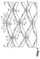
- the mesh 32 is formed by stamping a thin (5 mil) foil of high purity copper with a series of parallel overlapping slits. Once this is accomplished, the foil is expanded in a conventional manner by being pulled in opposite directions which are perpendicular to the lengthwise axes of the slits. The resultant pulling of the slits open (expanding) forms a somewhat diamond shaped mesh 32 shown in FIG. 3.
- the expanded mesh 32 includes diamond shaped openings 34 which are formed by perforating sheets of solid copper foil and then expanding the copper foil.
- Each opening 34 appears to be formed by two segments or "strands" of foil. These include (i) a first segment having an upper left portion 36 extending from a bend 38 in an upward and rightward direction (when viewing FIG. 3) where it joins with an upper right portion 40 at a bend 42 wherein the upper right portion 40 extends downward and rightward to a bend 44.
- the second segment of foil has a lower left portion 44 extending from a bend 46 in a downward and rightward direction where it joins with a lower right portion 48 at a bend 50 wherein the lower right portion 48 extends upward and rightward to a bend 52.
- each opening 34 is formed (i) at the nine o'clock position by a bottom edge of segment bend 38 which is connected to a top edge of segment bend 46 along a connection joint 53, and (ii) at the three o'clock position by a bottom edge of segment bend 44 which is connected to a top edge of segment bend 52 along a connection joint 55.
- a top edge of segment bend 42 is connected to a bottom edge of another segment bend 54 along a connection joint 57
- a bottom edge of segment bend 50 is connected to a top edge of another segment bend 56 along a connection joint 59.
- the individual segments of foil mesh do not lie in the same plane. That is, during the expansion process discussed above, the foil mesh 32 is formed into different planes. For example, assuming there is a first imaginary horizontal plane extending through connection line 53 (nine o'clock position), a top edge or peak 60 of segment bend 38 is located the farthest distance above this first imaginary horizontal plane, whereas a bottom edge or peak 62 of the adjoining bend 46 is located the farthest distance below this first imaginary horizontal plane.
- a top edge or peak 66 of segment bend 50 is located the farthest above this second imaginary horizontal plane, whereas a bottom edge or peak 68 of the adjoining segment bend 56 is located the farthest distance below this second imaginary horizontal plane.
- the resulting out of plane configuration of the foil mesh 32 creates a mesh of peaks 66,68 extending from opposite sides of the mesh.
- the expanded copper mesh 32 has a density of about .08 pounds per square foot and is sold under the product name "AstroStrike Screening" by the Astroseal Company of Old Saybrook, Connecticut. After expansion, normally this expanded mesh is rolled flat. However, for the purposes of the present invention, the flattening process is deleted so that the mesh retains its out-of-plane configuration shown in FIGS. 3 and 4.
- the conductive mesh 32 is taped over the joint 16 as shown in FIG. 2. It is preferable that the mesh 32 have a width dimension designated by the letter "w" in FIG. 2 of two inches or more in order to withstand the effects of a lightning strike.
- the mesh have a width dimension of about three inches so that it extends laterally beyond fasteners 20.
- the edges of the mesh are bent downward using pliers or the like to prevent curling so the mesh lays flat against the surface of the panel.
- the maximum resistance across a joint 16 which is one meter in length is about five milliohms. It is not necessary that an entire joint 16 between two adjacent panels be covered by the bridge 22, however. Rather, as shown in FIG. 2, spaces 62 (between consecutive bridges 22) which are small in relation to the wavelengths of the EMI and lightning strike energy are permissible. Since these wavelengths are on the order of about ten meters, spaces 62 of no more than about one meter between consecutive bridges 22 are permissible.
- an epoxy adhesive is brushed over the mesh in sufficient quantity that the entire mesh is covered with epoxy.
- the adhesive must be chemically compatible with the other materials used in the joint construction and is required to flow and envelop the conductive mesh 32 totally encasing it in resin. After cure, it is desirable that the conductive mesh be both physically and electrically isolated from the outer (air flow) side of the skin panel by the cured resin.
- the epoxy adhesive have the following properties: (1) it must be strong enough to maintain a high pressure contact between the bridge mesh 32 and the panel mesh 28; (2) it should be non-conductive so as to minimize the amount of heating within the resin when a lightning current flows through the conductive mesh; and (3) it should be sufficiently non-porous to protect the exposed embedded wire mesh 32 from mild impact damage and corrosion.
- the epoxy adhesive is Type EA 956 or EA 9396 manufactured by Hysol Corporation located in Pittsburgh, California.
- a Teflon® fabric parting film (not shown) is placed over the mesh 32.
- a fiberglass bleeder fabric 69 (FIG. 5) is applied over the parting film. The parting film prevents the bleeder fabric 69 from sticking to the mesh during curing.
- a nylon bag 70 which is attached via a tube 72 to a vacuum pump (not shown), is attached over the covered mesh 32 and secured to the panel by a conventional tape 74. Once this is accomplished, a vacuum of approximately twenty eight mm Hg is drawn for about twenty four hours to allow the adhesive to cure at room temperature.
- the peaks 66, 68 of the wire mesh 32 perform several valuable functions. First, the peaks contact the exposed mesh 28 of the panel 14 to make an electrical connection therewith. Also, during vacuum compression, the bridge mesh 32 is forced against the exposed panel mesh 28 causing any excess adhesive there between to be squeezed out. Beneath the peaks of the bridge mesh are open spaces 76 (FIG. 4) which provide paths for the adhesive to flow through. Without these paths for the adhesive to escape, there would be a tendency for the adhesive to prevent the peaks of the bridge mesh 32 from contacting the panel mesh 28 during vacuum compression thereby preventing proper electrical contact.
- the bridge mesh 32 remains in contact with the panel mesh 28 during the curing process.
- the conventional mesh might float away from the panel mesh 28 during the cure cycle.
- the conductive bridge of the present invention is placed across a joint between a composite panel or skin (identical to the panel 14) and a panel made of aluminum (not shown).
- the aluminum panel is prepared by exposing a bare aluminum portion of this panel. Typically, this is accomplished by removing any primer or other surface protectant from the surface of the aluminum skin by a sanding operation. Once this is accomplished, a protective coating is applied to the bare aluminum surface to prevent oxidation and to prepare the surface for the application of the adhesive.
- this coating is a chromate conversion coating formed by a chemical treatment of the aluminum in chemical solutions containing hexavalent chromium and goes by the name of Alodine.
- the aluminum surface is ready for the attachment of the bridge (identical to the bridge mesh 32) in the same manner discussed previously with regard to the attachment of the bridge mesh 32 to the exposed panel mesh 28. Furthermore, in this exemplary embodiment, the attachment of the bridge mesh to the composite panel is accomplished in the same manner as discussed previously with regard to the attachment of the bridge mesh 32 to the composite panel 14.
Landscapes
- Engineering & Computer Science (AREA)
- Aviation & Aerospace Engineering (AREA)
- Shielding Devices Or Components To Electric Or Magnetic Fields (AREA)
- Building Environments (AREA)
Applications Claiming Priority (2)
| Application Number | Priority Date | Filing Date | Title |
|---|---|---|---|
| US726041 | 1996-10-07 | ||
| US08/726,041 US5698316A (en) | 1996-10-07 | 1996-10-07 | Apparatus and methods of providing corrosion resistant conductive path across non conductive joints or gaps |
Publications (2)
| Publication Number | Publication Date |
|---|---|
| EP0835049A2 true EP0835049A2 (fr) | 1998-04-08 |
| EP0835049A3 EP0835049A3 (fr) | 1998-07-22 |
Family
ID=24916976
Family Applications (1)
| Application Number | Title | Priority Date | Filing Date |
|---|---|---|---|
| EP19970202940 Withdrawn EP0835049A3 (fr) | 1996-10-07 | 1997-09-25 | Appareil et méthode pour réaliser un chemin conducteur résistant à la corrosion à travers des joints ou des interstices non conducteurs |
Country Status (3)
| Country | Link |
|---|---|
| US (1) | US5698316A (fr) |
| EP (1) | EP0835049A3 (fr) |
| CA (1) | CA2215117C (fr) |
Cited By (4)
| Publication number | Priority date | Publication date | Assignee | Title |
|---|---|---|---|---|
| DE102007062111A1 (de) * | 2007-12-21 | 2009-07-02 | Airbus Deutschland Gmbh | Abschirmanordnung für insbesondere elektrische Leitungen in Flugzeugen |
| US8167231B2 (en) | 2007-12-21 | 2012-05-01 | Airbus Deutschland Gmbh | Shielding arrangement for lines, in particular electrical lines, in aircraft |
| US20250074626A1 (en) * | 2023-08-31 | 2025-03-06 | Airbus Operations Sas | Method for repairing a structural part of an aircraft having a protection defect, and structural aircraft part thus repaired |
| US12612187B2 (en) * | 2023-08-31 | 2026-04-28 | Airbus Operations Sas | Method for repairing a structural part of an aircraft having a protection defect, and structural aircraft part thus repaired |
Families Citing this family (25)
| Publication number | Priority date | Publication date | Assignee | Title |
|---|---|---|---|---|
| NL1007018C2 (nl) * | 1997-09-11 | 1999-03-12 | Hollandse Signaalapparaten Bv | Vezel-kunststof composiet lichaam voor electromagnetische afscherming, voorzien van een elektrische contactstrip. |
| GB9807198D0 (en) * | 1998-04-04 | 1998-06-03 | British Aerospace | Adhesively bonded joints in carbon fibre composite structures |
| US6284175B1 (en) * | 1999-04-29 | 2001-09-04 | Northrop Grumman Corporation | Method for reducing reflected radio frequency electromagnetic radiation |
| ES2264299B1 (es) * | 2003-06-06 | 2007-11-16 | Airbus España S.L. | Sistema de proteccion contra rayos para depositos de combustible fabricados en materiales compuestos de pobre conductividad electrica. |
| JP5610662B2 (ja) * | 2003-09-30 | 2014-10-22 | ザ・ボーイング・カンパニーTheBoeing Company | 保護シート |
| US7052573B2 (en) * | 2003-11-21 | 2006-05-30 | The Boeing Company | Method to eliminate undulations in a composite panel |
| US7554785B2 (en) * | 2004-03-23 | 2009-06-30 | The Boeing Company | Lightning damage protection for composite aircraft |
| US7561402B2 (en) | 2006-02-24 | 2009-07-14 | The Boeing Company | Gap lightning surface protection of composite structures |
| US7790294B2 (en) * | 2006-07-05 | 2010-09-07 | Lockheed Martin Corporation | System, method, and apparatus for three-dimensional woven metal preform structural joint |
| DE102006050534B4 (de) * | 2006-10-26 | 2013-12-12 | Airbus Operations Gmbh | Leitungssystem für ein Luftfahrzeug, insbesondere ein Flugzeug |
| US7642975B2 (en) * | 2008-03-12 | 2010-01-05 | Sikorsky Aircraft Corporation | Frame assembly for electrical bond |
| US8201773B1 (en) | 2008-07-02 | 2012-06-19 | The United States Of America As Represented By Secretary Of The Navy | Flexible self-erecting substructures for sensor networks |
| FR2941919B1 (fr) * | 2009-02-11 | 2011-04-08 | Airbus France | Element de reseau de retour de courant pour aeronef |
| US8222541B2 (en) * | 2009-06-19 | 2012-07-17 | General Electric Company | Avionics chassis |
| US8059409B2 (en) * | 2009-06-19 | 2011-11-15 | General Electric Company | Avionics chassis |
| US7911796B2 (en) * | 2009-06-19 | 2011-03-22 | General Electric Company | Avionics chassis |
| US8023267B2 (en) * | 2009-06-19 | 2011-09-20 | General Electric Company | Avionics chassis |
| US9415854B2 (en) * | 2011-09-14 | 2016-08-16 | Mitsubishi Aircraft Corporation | Aircraft window and aircraft having an electromagnetic shield |
| US9484123B2 (en) | 2011-09-16 | 2016-11-01 | Prc-Desoto International, Inc. | Conductive sealant compositions |
| JP6171402B2 (ja) * | 2013-03-01 | 2017-08-02 | セイコーエプソン株式会社 | モジュール、電子機器、および移動体 |
| EP2971610B1 (fr) * | 2013-03-15 | 2020-01-15 | United Technologies Corporation | Enlèvement ou masquage sélectif de revêtement pour une piste de mise à la terre |
| EP3130196A4 (fr) | 2014-04-10 | 2017-12-06 | Metis Design Corporation | Ensembles multifonctionnels |
| EP3234231B8 (fr) * | 2014-12-17 | 2020-11-04 | BAE Systems PLC | Traitement d'objets par revêtement par traitement chimique |
| US10875663B2 (en) * | 2017-12-11 | 2020-12-29 | The Boeing Company | Lightning protection in aircrafts constructed with carbon fiber reinforced plastic |
| EP4659953A1 (fr) * | 2024-06-04 | 2025-12-10 | AIRBUS Operations GmbH | Composant structurel, procédé de fabrication d'un composant structurel et aéronef |
Family Cites Families (17)
| Publication number | Priority date | Publication date | Assignee | Title |
|---|---|---|---|---|
| US3431348A (en) * | 1966-05-06 | 1969-03-04 | Tech Wire Prod Inc | Electromagnetic shield and viewing laminate |
| US3755713A (en) * | 1972-07-25 | 1973-08-28 | Boeing Co | Electrically conductive surface for aircraft |
| US4015035A (en) * | 1972-08-10 | 1977-03-29 | Lockheed Aircraft Corporation | Method of forming fiber-reinforced epoxy composite joints, and product thereof |
| US3885071A (en) * | 1972-08-10 | 1975-05-20 | Lockheed Aircraft Corp | Fiber-reinforced epoxy composite joints |
| US4313777A (en) * | 1979-08-30 | 1982-02-02 | The United States Of America As Represented By The United States National Aeronautics And Space Administration | One-step dual purpose joining technique |
| SE446924B (sv) * | 1985-02-22 | 1986-10-13 | Devex Sa | Sett vid utforande av en for elektromagnetisk stralning vesentligen opak skerm |
| US4671470A (en) * | 1985-07-15 | 1987-06-09 | Beech Aircraft Corporation | Method for fastening aircraft frame elements to sandwich skin panels covering same using woven fiber connectors |
| US4746389A (en) * | 1987-08-04 | 1988-05-24 | United Technologies Corporation | Method for producing a clean, highly conductive surface for mating composite articles |
| US5127601A (en) * | 1989-01-23 | 1992-07-07 | Lightning Diversion Systems | Conformal lightning shield and method of making |
| US4977296A (en) * | 1989-02-23 | 1990-12-11 | Hemming Leland H | Radio frequency shielding tape |
| US5250342A (en) * | 1989-05-24 | 1993-10-05 | United Technologies Corporation | Composite EMI shield having clean, highly conductive surfaces for conductive bonding |
| US5065960A (en) * | 1990-02-05 | 1991-11-19 | Northrop Corporation | Gap filler for advanced aircraft to reduce radar detectability |
| US5239125A (en) * | 1990-06-19 | 1993-08-24 | The United States Of America As Represented By The Secretary Of The Army | EMI/RFI shield |
| US5370921A (en) * | 1991-07-11 | 1994-12-06 | The Dexter Corporation | Lightning strike composite and process |
| US5595801A (en) * | 1991-07-30 | 1997-01-21 | International Paper Company | Laminated shielding material and method for shielding an enclosure therewith |
| JP2713059B2 (ja) * | 1992-10-07 | 1998-02-16 | 三菱電機株式会社 | 電子部品または電子機器を収納する箱または蓋からなる筺体の製造方法。 |
| US5312508A (en) * | 1992-10-16 | 1994-05-17 | John Chisholm | Attaching crimped wire mesh to an object requiring heat transfer |
-
1996
- 1996-10-07 US US08/726,041 patent/US5698316A/en not_active Expired - Lifetime
-
1997
- 1997-09-11 CA CA 2215117 patent/CA2215117C/fr not_active Expired - Lifetime
- 1997-09-25 EP EP19970202940 patent/EP0835049A3/fr not_active Withdrawn
Cited By (4)
| Publication number | Priority date | Publication date | Assignee | Title |
|---|---|---|---|---|
| DE102007062111A1 (de) * | 2007-12-21 | 2009-07-02 | Airbus Deutschland Gmbh | Abschirmanordnung für insbesondere elektrische Leitungen in Flugzeugen |
| US8167231B2 (en) | 2007-12-21 | 2012-05-01 | Airbus Deutschland Gmbh | Shielding arrangement for lines, in particular electrical lines, in aircraft |
| US20250074626A1 (en) * | 2023-08-31 | 2025-03-06 | Airbus Operations Sas | Method for repairing a structural part of an aircraft having a protection defect, and structural aircraft part thus repaired |
| US12612187B2 (en) * | 2023-08-31 | 2026-04-28 | Airbus Operations Sas | Method for repairing a structural part of an aircraft having a protection defect, and structural aircraft part thus repaired |
Also Published As
| Publication number | Publication date |
|---|---|
| EP0835049A3 (fr) | 1998-07-22 |
| CA2215117A1 (fr) | 1998-04-07 |
| US5698316A (en) | 1997-12-16 |
| CA2215117C (fr) | 2003-07-08 |
Similar Documents
| Publication | Publication Date | Title |
|---|---|---|
| US5698316A (en) | Apparatus and methods of providing corrosion resistant conductive path across non conductive joints or gaps | |
| US7554785B2 (en) | Lightning damage protection for composite aircraft | |
| US7277266B1 (en) | Lightning protection system for composite structure | |
| EP1767344B2 (fr) | Recouvrement parafoudre pour une surface étendue | |
| US3989984A (en) | Aircraft lightning protection means | |
| US5127601A (en) | Conformal lightning shield and method of making | |
| US7525785B2 (en) | Lightning strike protection method and apparatus | |
| EP1673218B1 (fr) | Autocollant de protection et son utilisation | |
| US8687342B2 (en) | Method of surface charge distribution | |
| RU2465176C2 (ru) | Система отвода тока молнии, генерируемого грозовым разрядом на летательный аппарат | |
| CA1316232C (fr) | Mecanisme assurant la continuite electrique dans les joints composes | |
| CN101282834B (zh) | 用于飞行器外部防护的环境稳定的混合织物系统 | |
| RU2676623C1 (ru) | Композитная структура | |
| CA2100241A1 (fr) | Element de structure | |
| CN105460228B (zh) | 飞行器中使用的导电热塑性接地平面 | |
| US20070141927A1 (en) | Method and system for exterior protection of an aircraft | |
| EP3156321B1 (fr) | Raidisseur composite avec élément conducteur intégré | |
| CN112072335A (zh) | 一种复合材料结构件之间导电结构及导电处理方法 | |
| US7776769B2 (en) | Manufacture and assembly of structures | |
| JP2001088793A (ja) | 複合材構造体及びこれを用いた航空尾翼 | |
| GB2545655A (en) | A structure formed from composite material | |
| US20250375946A1 (en) | Method for repairing composite structures for improved electromagnetic effects (eme) protection | |
| US12089388B2 (en) | Composite material structure | |
| Heseltine et al. | Electrical connections and antenna performance of a large composite | |
| CN114180083A (zh) | 一种利用铜杯实现的复合材料结构件之间导电处理方法 |
Legal Events
| Date | Code | Title | Description |
|---|---|---|---|
| PUAI | Public reference made under article 153(3) epc to a published international application that has entered the european phase |
Free format text: ORIGINAL CODE: 0009012 |
|
| AK | Designated contracting states |
Kind code of ref document: A2 Designated state(s): DE FR GB IT |
|
| PUAL | Search report despatched |
Free format text: ORIGINAL CODE: 0009013 |
|
| AK | Designated contracting states |
Kind code of ref document: A3 Designated state(s): AT BE CH DE DK ES FI FR GB GR IE IT LI LU MC NL PT SE |
|
| 17P | Request for examination filed |
Effective date: 19990119 |
|
| AKX | Designation fees paid |
Free format text: DE FR GB IT |
|
| RBV | Designated contracting states (corrected) |
Designated state(s): DE FR GB IT |
|
| 17Q | First examination report despatched |
Effective date: 20040225 |
|
| STAA | Information on the status of an ep patent application or granted ep patent |
Free format text: STATUS: THE APPLICATION IS DEEMED TO BE WITHDRAWN |
|
| 18D | Application deemed to be withdrawn |
Effective date: 20041009 |