EP0835497B1 - Carte a puce - Google Patents
Carte a puce Download PDFInfo
- Publication number
- EP0835497B1 EP0835497B1 EP96918600A EP96918600A EP0835497B1 EP 0835497 B1 EP0835497 B1 EP 0835497B1 EP 96918600 A EP96918600 A EP 96918600A EP 96918600 A EP96918600 A EP 96918600A EP 0835497 B1 EP0835497 B1 EP 0835497B1
- Authority
- EP
- European Patent Office
- Prior art keywords
- metal
- contact surfaces
- layer
- metallization
- plastic substrate
- Prior art date
- Legal status (The legal status is an assumption and is not a legal conclusion. Google has not performed a legal analysis and makes no representation as to the accuracy of the status listed.)
- Expired - Lifetime
Links
Images





Classifications
-
- C—CHEMISTRY; METALLURGY
- C23—COATING METALLIC MATERIAL; COATING MATERIAL WITH METALLIC MATERIAL; CHEMICAL SURFACE TREATMENT; DIFFUSION TREATMENT OF METALLIC MATERIAL; COATING BY VACUUM EVAPORATION, BY SPUTTERING, BY ION IMPLANTATION OR BY CHEMICAL VAPOUR DEPOSITION, IN GENERAL; INHIBITING CORROSION OF METALLIC MATERIAL OR INCRUSTATION IN GENERAL
- C23C—COATING METALLIC MATERIAL; COATING MATERIAL WITH METALLIC MATERIAL; SURFACE TREATMENT OF METALLIC MATERIAL BY DIFFUSION INTO THE SURFACE, BY CHEMICAL CONVERSION OR SUBSTITUTION; COATING BY VACUUM EVAPORATION, BY SPUTTERING, BY ION IMPLANTATION OR BY CHEMICAL VAPOUR DEPOSITION, IN GENERAL
- C23C2/00—Hot-dipping or immersion processes for applying the coating material in the molten state without affecting the shape; Apparatus therefor
- C23C2/04—Hot-dipping or immersion processes for applying the coating material in the molten state without affecting the shape; Apparatus therefor characterised by the coating material
-
- C—CHEMISTRY; METALLURGY
- C25—ELECTROLYTIC OR ELECTROPHORETIC PROCESSES; APPARATUS THEREFOR
- C25D—PROCESSES FOR THE ELECTROLYTIC OR ELECTROPHORETIC PRODUCTION OF COATINGS; ELECTROFORMING; APPARATUS THEREFOR
- C25D5/00—Electroplating characterised by the process; Pretreatment or after-treatment of workpieces
- C25D5/02—Electroplating of selected surface areas
- C25D5/022—Electroplating of selected surface areas using masking means
-
- C—CHEMISTRY; METALLURGY
- C25—ELECTROLYTIC OR ELECTROPHORETIC PROCESSES; APPARATUS THEREFOR
- C25D—PROCESSES FOR THE ELECTROLYTIC OR ELECTROPHORETIC PRODUCTION OF COATINGS; ELECTROFORMING; APPARATUS THEREFOR
- C25D5/00—Electroplating characterised by the process; Pretreatment or after-treatment of workpieces
- C25D5/22—Electroplating combined with mechanical treatment during the deposition
-
- C—CHEMISTRY; METALLURGY
- C25—ELECTROLYTIC OR ELECTROPHORETIC PROCESSES; APPARATUS THEREFOR
- C25D—PROCESSES FOR THE ELECTROLYTIC OR ELECTROPHORETIC PRODUCTION OF COATINGS; ELECTROFORMING; APPARATUS THEREFOR
- C25D7/00—Electroplating characterised by the article coated
-
- G—PHYSICS
- G06—COMPUTING OR CALCULATING; COUNTING
- G06K—GRAPHICAL DATA READING; PRESENTATION OF DATA; RECORD CARRIERS; HANDLING RECORD CARRIERS
- G06K19/00—Record carriers for use with machines and with at least a part designed to carry digital markings
- G06K19/04—Record carriers for use with machines and with at least a part designed to carry digital markings characterised by the shape
-
- G—PHYSICS
- G06—COMPUTING OR CALCULATING; COUNTING
- G06K—GRAPHICAL DATA READING; PRESENTATION OF DATA; RECORD CARRIERS; HANDLING RECORD CARRIERS
- G06K19/00—Record carriers for use with machines and with at least a part designed to carry digital markings
- G06K19/06—Record carriers for use with machines and with at least a part designed to carry digital markings characterised by the kind of the digital marking, e.g. shape, nature, code
- G06K19/067—Record carriers with conductive marks, printed circuits or semiconductor circuit elements, e.g. credit or identity cards also with resonating or responding marks without active components
- G06K19/07—Record carriers with conductive marks, printed circuits or semiconductor circuit elements, e.g. credit or identity cards also with resonating or responding marks without active components with integrated circuit chips
- G06K19/077—Constructional details, e.g. mounting of circuits in the carrier
- G06K19/07743—External electrical contacts
-
- G—PHYSICS
- G06—COMPUTING OR CALCULATING; COUNTING
- G06K—GRAPHICAL DATA READING; PRESENTATION OF DATA; RECORD CARRIERS; HANDLING RECORD CARRIERS
- G06K19/00—Record carriers for use with machines and with at least a part designed to carry digital markings
- G06K19/06—Record carriers for use with machines and with at least a part designed to carry digital markings characterised by the kind of the digital marking, e.g. shape, nature, code
- G06K19/08—Record carriers for use with machines and with at least a part designed to carry digital markings characterised by the kind of the digital marking, e.g. shape, nature, code using markings of different kinds or more than one marking of the same kind in the same record carrier, e.g. one marking being sensed by optical and the other by magnetic means
- G06K19/083—Constructional details
-
- H—ELECTRICITY
- H10—SEMICONDUCTOR DEVICES; ELECTRIC SOLID-STATE DEVICES NOT OTHERWISE PROVIDED FOR
- H10W—GENERIC PACKAGES, INTERCONNECTIONS, CONNECTORS OR OTHER CONSTRUCTIONAL DETAILS OF DEVICES COVERED BY CLASS H10
- H10W72/00—Interconnections or connectors in packages
- H10W72/851—Dispositions of multiple connectors or interconnections
- H10W72/874—On different surfaces
- H10W72/884—Die-attach connectors and bond wires
-
- H—ELECTRICITY
- H10—SEMICONDUCTOR DEVICES; ELECTRIC SOLID-STATE DEVICES NOT OTHERWISE PROVIDED FOR
- H10W—GENERIC PACKAGES, INTERCONNECTIONS, CONNECTORS OR OTHER CONSTRUCTIONAL DETAILS OF DEVICES COVERED BY CLASS H10
- H10W90/00—Package configurations
- H10W90/701—Package configurations characterised by the relative positions of pads or connectors relative to package parts
- H10W90/751—Package configurations characterised by the relative positions of pads or connectors relative to package parts of bond wires
- H10W90/754—Package configurations characterised by the relative positions of pads or connectors relative to package parts of bond wires between a chip and a stacked insulating package substrate, interposer or RDL
Definitions
- the invention relates to a method for the production of chip modules for contact-type chip cards, which have such a chip module (carrier element for the IC chip / chip) with electrically conductive contact surfaces. These contact surfaces are electrically connected to corresponding connection points of the IC module, so that in this case the communication of the IC module with appropriate devices (chip card terminals / machines) is possible.
- the chip module is fixed in a recess of the card body that is open toward the front of the card.
- the surface of the chip module is formed by a structured, the electrically conductive contact surfaces forming metallization with insulating gaps (lines).
- the contact surfaces are arranged offset in the plane of the front of the card or minimal (about ⁇ 0.1 mm) with respect to this.
- Such smart cards have already found widespread use in the form of telephone cards, health insurance cards, GSM cards, bank cards and credit cards.
- the layout of these cards is designed in a complex way.
- the visible surface of the chip module with its contact surfaces acts as a foreign body in the layout of the card front side, whereby the visual appearance is adversely affected and the layout Horsdorfkeiten are impaired.
- the contact surfaces have either a metallization of gold, silver or palladium, wherein the palladium metallization appears silver.
- These metals are particularly well suited for the formation of contact surfaces, as they are very chemically very are inert, ie in particular not oxidize or corrode, and with them on the other hand, very low contact resistance to the contacts of the smart card terminal can be achieved.
- gold and palladium, especially with special alloy additives have a high wear resistance. For these reasons, today almost exclusively gold or palladium is used for the contact surfaces of smart cards. Thus, there is only the choice between a chip module with gold or silver-colored surface for the layout design.
- WO 94/02 912 is a arranged on a memory card contact field is known, which is provided with an integrated, electrically conductive presentation icon, for example in the form of a post horn. This is intended to improve the anti-counterfeiting security of the memory card, as a counterfeiter is not easily able to accommodate the display icon in the contact field.
- the placement of the character or display symbol in the contact field is done with a corresponding mask.
- a colored adhesive layer serves here for fixing a chip module.
- the object of the invention is therefore to provide a further method for the production of chip modules for smart cards, in which the surface of the chip module can be adapted to the "layout design of the card front side, ie can be included as a design surface, so that the design possibilities for the visual appearance of the chip card are extended.
- FIGS. 12 to 14 represented objects do not belong to the claimed invention, but serve only to facilitate the understanding of the invention:
- FIG. 1 shows a plan view of the front side of a standard chip card (1) with the embedded therein chip module (2) and its electrical contact surfaces (20A).
- FIG. 2 is an enlarged section of the map (1) in FIG. 1 in the area of the chip module (2).
- the surface of the chip module (2) is formed by a structured metallization (20) having insulating interspaces (lines, 22A) forming the electrically conductive contact surfaces (20A).
- FIGS. 3 and 4 show the corresponding one with a different structuring of the contact surfaces (20A).
- the copper layer typically has a thickness of 35 .mu.m, the nickel layer a thickness of 15 .mu.m and the gold or palladium layer a thickness of 2 .mu.m.
- the color of the contact surfaces (20A) is deliberately adjusted by introducing this intermediate into a dyeing bath (dyeing solution).
- the color of the contact surfaces (20A) is brought about by a chemical reaction on the surface and / or in the near-surface region of the metallization (20) (reaction layer thickness ⁇ 1 ⁇ m). This can be done in a pure dipping process, ie without the use of an external power source, or in an electrolytic / galvanic process, ie be realized using an external power source.
- the following dyeing solution can be used for the green coloration of a gold contact surface: (see, for example: Handbook of Electroplating, Carl Hanser Verlag, Kunststoff 1969, Volume III, pages 291,292 ) Potassium nitrate (30% by weight) KNO 3 Iron (II) sulfate (10% by weight) FeSO 4 * 7H 2 O Zinc sulphate (5% by weight) ZnS0 4 * 7H 2 O Potassium aluminum sulfate (5% by weight) KAl (S0 4) 2 * 12H 2 O Water (50% by weight) H 2 O
- Dyeing parameters such as temperature, dyeing time, stirring (convection) must be optimally adapted to the specific conditions; By using in each case special dyeing solutions a total of a broad color spectrum can thus be covered.
- Coloring is not limited to gold, palladium or silver contact surfaces. Likewise, other metallizations (20) can be discolored and used as an outer contact surface layer.
- the coloring does not adversely affect functional properties such as chemical resistance, conductivity, abrasion resistance and light resistance.
- contact surfaces (20A) in the so-called lead frame technique.
- the metallization (20) forming the contact surfaces (20A) is not applied to a plastic substrate.
- the metallization of the chip module has at least two areas whose visible layer is formed of different metals and / or metal alloys, each with different light reflection and absorption properties.
- the procedure is as follows: A plastic substrate serving for the production of chip modules (2), on which a base metallization (201, 202) is applied for a plurality of chip modules, is introduced into a galvanic bath, where the different areas (20 *, 20 **) are each formed by galvanic deposition using selective coverage (passivation).
- FIG. 18 an enlarged section of the card (1) in the region of the chip module (2) is shown.
- the surface of the chip module is formed by a structured, the electrically conductive contact surfaces (20A) forming metallization (20).
- the metallization has two areas of different metals and / or metal alloys with different light reflection and absorption properties.
- FIG. 19 a layer structure of the metallization (20) is shown.
- a layer (202) On a non-conductive plastic substrate (22) with a laminated copper layer (201) as a diffusion barrier, a layer (202), for example a nickel layer, electrodeposited. With the aid of selective coverage (passivation) by photoresist, it is possible to apply different metals and / or metal alloys to different surface areas (20 *, 20 **) of the nickel layer (202).
- the base metalization may also be formed by three layers (eg copper, nickel and gold).
- the second area (20 **) is raised from the first one.
- the raised, second surface area is once as a company logo ( fig.20 ) and the other time as a currency symbol (Fig.21).
- a first metal or metal alloy layer (20 *) with specific light reflection and absorption properties is applied over the entire area to the base metalization (201, 202) in a first step.
- the first surface area (20 *) is raised in relation to the second area area (20 **).
- a first metal or metal alloy layer with specific light reflection and absorption properties is applied over the entire area to the base metalization (201, 202) in a first step.
- a second metal or metal alloy layer with light reflection and absorption properties that is different from the first metal or metal alloy layer is then applied over the entire surface of the first metal or metal alloy layer to form the second surface region (20 **).
- the second metal or metal alloy layer (20 **) is removed locally by an electrochemical process (e.g., an etch) so that the underlying first metal or metal alloy layer becomes visible.
- ISO 7816-2 specifies the position and minimum size of standard contact surfaces (20B), after which the standard contact surfaces (20B) must not be less than 2mm * 1.7mm. These standard contact surfaces (20B) are in FIG. 2 and 4 dashed lines.
- insulating gaps (lines 22A) are provided in the metallization (20).
- a colored plastic substrate (21) is now used, which is visible through the insulating, clear intermediate spaces (lines, 22A) (cf. Figure 9 ). Colored in this sense may also be a fluorescent plastic substrate (21).
- PVC polyvinyl chloride
- polyethylene polyethylene
- glass fiber reinforced epoxy resin or the like.
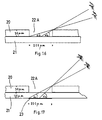
- this total shading angle is 16 °, ie in a viewing angle range from the vertical view (90 °) to a viewing angle of 16 °, the colored plastic substrate ( 21) at least partially visible.
- L2 the viewpoint at which a semi-shading has occurred.
- further clear spaces (22B) may be provided, through which the colored plastic substrate (21) is likewise visible.
- FIG. 5 a section of a plan view of a chip card (1) with a guilloche pattern (3) is shown.
- the lines forming the guilloche pattern (3) continue on the metallization (20) forming the contact surfaces (20A) as insulating lines (22A) between the standard contact surfaces (20B). If, for example, the color red is selected for the lines (3) printed on the card body (1A), a red plastic substrate (21) is accordingly taken.
- a uniform color behind the guilloche pattern (3) can then be achieved on the entire card side, including the chip module surface.
- the surface of the chip module (2) is thus integrated in the card layout and does not represent a foreign body. In addition, this provides a considerable degree of additional security against counterfeiting, since this chip module (2) with its very specially structured for a card type and color-designed surface, would suspect, if it is inserted into another card body.
- the motif is a wheel with spokes, with the spokes continuing as insulating gaps (lines, 22A) between the standard contact surfaces (1A).
- a color matching between the printed on the card body (1A) motif portions and the motif portions on the surface of the chip module (2) is easily possible.
- FIG. 7 another layout design is shown.
- the motif here is a company logo, wherein on both sides of the chip module (2) a letter is printed on the front of the card and the other two letters are formed by additional spaces (22B) in the metallization (20).
- additional spaces (22B) in the metallization (20) By choosing a correspondingly colored plastic substrate (21), color matching is also possible without any problem here.
- the plastic substrate (21) is completely or partially transparent. On the side facing away from the metallization (20) side (back) of the plastic substrate (21) while one or more color pattern (23) are applied, so that the color pattern (23) through the plastic substrate (21) and the clear spaces ( 22A, 22B) are visible (see. Fig. 8 . 15 . 17 ).
- FIG. 8 is a layout design shown, which is technically feasible with this design variant. As a motive, the Olympic rings are chosen, with two ring segments continuing as insulating gaps (lines, 22A) on the metallization (20). The on the back of the plastic substrate (21) applied ring segments are formed in different colors.
- the rear side of the plastic substrate (21) is printed gold-colored, which corresponds to the color of the gold contact surfaces (20A). corresponds, so that these spaces (lines, 22A) do not settle in color from the metallization (20). In this way, the chip module (2) can hide in the card layout.
- the color patterns (23) can also be printed or sputtered onto the backside of the plastic substrate (21).
- ink (24) is introduced into the insulating interspaces (lines, 22A) in the metallization (20) (cf. Figure 11 ).
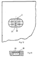
- the metallization (20) forming the contact surfaces (20A) has a raised geometry (25) in the ⁇ m for selectively influencing the light reflection and / or sub-micron range, which may be embossed in the metallization (20) or may be formed by electrodeposition.
- FIG. 12 shows, for example, a company logo, which is present as a raised structure (25) on the metallization (25).
- FIG. 13 shows a section through the chip card (1) in the region of this raised structure (25).
- the sublime structures (25) may also be formed as a surface relief corresponding to a rainbow hologram. Also, for example, scale-like structures are possible, which produce multicolored iridescent light reflections (cf. Fig. 14 ).
- a chip module (2) implanted in a card body (1) is shown.
- the chip module (2) consists of the contact surfaces (20A) which are electrically conductively connected to connection points (26A) of the IC chip (26) via bonding wires (27).
- the IC module (26) and the bonding wires (27) and the connection points (26A) of the bonding wires () on the IC module (26) and on the contact surfaces (20A) are protected against mechanical stress, oxidation and moisture with a potting compound (28) surrounded.
- the IC module (26) is inserted in a central recess of the plastic substrate (21) and fixed with an adhesive, preferably an electrically conductive adhesive, on a ground-related contact surface (20A).
- the plastic substrate 21 has contact access openings 29A.
- the chip module (2) is fixed with a hot-melt adhesive layer (4) in a recess (1B) of the card body (1A).
- This hot-melt adhesive layer (4) can also be dyed according to the invention.
- the IC module (26) is fixed on the plastic substrate (21).
- the bonding wires (27) are electrically connected to the contact surfaces (20A) by means of plated-through holes (29B).
Landscapes
- Engineering & Computer Science (AREA)
- Chemical & Material Sciences (AREA)
- Organic Chemistry (AREA)
- Materials Engineering (AREA)
- Metallurgy (AREA)
- Chemical Kinetics & Catalysis (AREA)
- Electrochemistry (AREA)
- Physics & Mathematics (AREA)
- General Physics & Mathematics (AREA)
- Theoretical Computer Science (AREA)
- Mechanical Engineering (AREA)
- Computer Hardware Design (AREA)
- Microelectronics & Electronic Packaging (AREA)
- Credit Cards Or The Like (AREA)
Claims (2)
- Procédé de fabrication de modules de puce pour cartes à puce, dans lequel un substrat de matière plastique servant à la fabrication de modules de puce (2), sur lequel est appliqué une métallisation de base (201, 202) pour une pluralité de modules de puce, est placé dans un bain galvanique et les différentes zones de la surface (20*, 20**) sont formées par dépôt galvanique à l'aide d'un recouvrement sélectif (passivation), dans lequel, dans une première étape, une première couche d'un métal ou d'un alliage métallique offrant des caractéristiques prédéterminées de réflexion lumineuse et d'absorption sur toute la surface par un dépôt galvanique sur la métallisation de base (201, 202), dans une deuxième étape, une deuxième couche de métal ou d'alliage métallique offrant des caractéristiques de réflexion lumineuse et d'absorption différentes de celles de la première, est appliquée galvaniquement sur toute la surface ou seulement sur une partie de la surface de la première couche de métal ou d'alliage métallique et, dans une troisième étape, la deuxième couche de métal ou d'alliage métallique est éliminée localement par un processus électrochimique, si bien que la première couche de métal ou d'alliage métallique sous-jacente est visible.
- Procédé selon la revendication 1, caractérisé en ce que la métallisation de base (201, 202) est formée d'une couche de cuivre et d'une couche de nickel placée au-dessus.
Applications Claiming Priority (5)
| Application Number | Priority Date | Filing Date | Title |
|---|---|---|---|
| DE19523242A DE19523242A1 (de) | 1995-06-27 | 1995-06-27 | Chipkarte |
| DE19523242 | 1995-06-27 | ||
| DE19532223A DE19532223C1 (de) | 1995-09-01 | 1995-09-01 | Chipkarte |
| DE19532223 | 1995-09-01 | ||
| PCT/DE1996/001105 WO1997001823A2 (fr) | 1995-06-27 | 1996-06-24 | Carte a puce |
Publications (2)
| Publication Number | Publication Date |
|---|---|
| EP0835497A2 EP0835497A2 (fr) | 1998-04-15 |
| EP0835497B1 true EP0835497B1 (fr) | 2013-03-27 |
Family
ID=26016298
Family Applications (1)
| Application Number | Title | Priority Date | Filing Date |
|---|---|---|---|
| EP96918600A Expired - Lifetime EP0835497B1 (fr) | 1995-06-27 | 1996-06-24 | Carte a puce |
Country Status (4)
| Country | Link |
|---|---|
| US (1) | US6259035B1 (fr) |
| EP (1) | EP0835497B1 (fr) |
| ES (1) | ES2408855T3 (fr) |
| WO (1) | WO1997001823A2 (fr) |
Families Citing this family (33)
| Publication number | Priority date | Publication date | Assignee | Title |
|---|---|---|---|---|
| US5997654A (en) | 1995-06-27 | 1999-12-07 | The Procter & Gamble Company | Cleaning/sanitizing methods, compositions, and/or articles for produce |
| DE19630049A1 (de) * | 1996-07-25 | 1998-01-29 | Siemens Ag | Chipkarte mit einer Kontaktzone und Verfahren zum Herstellen einer solchen Kontaktzone |
| DE19833103C1 (de) * | 1998-07-23 | 1999-08-26 | Orga Kartensysteme Gmbh | Chipkarten, Verfahren zur Herstellung derselben, Zwischenerzeugnis sowie System zur Prüfung der Echtheit derart hergestellter Chipkarten |
| US20050061539A1 (en) * | 2003-09-19 | 2005-03-24 | Mirov Russell Norman | Mechanism for disabling an electronic assembly |
| DE10345257B4 (de) * | 2003-09-29 | 2008-10-02 | Infineon Technologies Ag | Chipkarte mit Kontaktfelder und Verfahren zum Herstellen solcher Kontaktfelder |
| DE102004021872B3 (de) * | 2004-05-04 | 2005-12-22 | Infineon Technologies Ag | Chipkarte, Verfahren zum Herstellen einer Chipkarte und elektrisch leitfähiges Kontaktierungselement |
| DE102008028300B4 (de) * | 2008-06-13 | 2021-10-07 | Tdk Electronics Ag | Leiterplatte mit flexiblem Bereich und Verfahren zur Herstellung |
| FR2932910B1 (fr) * | 2008-06-20 | 2011-02-11 | Smart Packaging Solutions Sps | Carte sans contact avec logo securitaire |
| EP2339511A1 (fr) * | 2009-12-17 | 2011-06-29 | Gemalto SA | Objet communicant avec sécurisation d'une interface de communication par contact |
| EP2390824A1 (fr) * | 2010-05-27 | 2011-11-30 | Gemalto SA | Procédé de réalisation d'un module multifonctionnel et dispositif le comprenant |
| US20150129665A1 (en) * | 2013-11-13 | 2015-05-14 | David Finn | Connection bridges for dual interface transponder chip modules |
| EP2642430A1 (fr) * | 2012-03-22 | 2013-09-25 | Gemalto SA | Carte à puce et procédé de fabrication |
| FR2989492B1 (fr) * | 2012-04-17 | 2014-12-26 | Microconnections Sas | Procede de marquage de module de carte a puce par electrodeposition |
| FR2989491B1 (fr) | 2012-04-17 | 2014-12-26 | Microconnections Sas | Procede de marquage de module de carte a puce par gravure |
| FR2997550B1 (fr) * | 2012-10-26 | 2016-01-22 | Linxens Holding | Circuit electrique, module electronique pour carte a puce realise sur ce circuit electrique et procede pour la realisation d’un tel circuit electrique. |
| FR3000583B1 (fr) * | 2012-12-31 | 2016-02-05 | Smart Packaging Solutions | Carte a puce avec element securitaire reparti entre corps de carte et module |
| FR3016442B1 (fr) * | 2014-01-10 | 2017-07-21 | Continental Automotive France | Mesure de resistances de reprise de contacts |
| US11068770B2 (en) | 2014-03-08 | 2021-07-20 | Féinics AmaTech Teoranta Lower Churchfield | Connection bridges for dual interface transponder chip modules |
| WO2015154019A2 (fr) | 2014-04-04 | 2015-10-08 | Visa International Service Association | Dispositif de paiement avec élément de sécurité holographique |
| GB201510252D0 (en) * | 2015-06-12 | 2015-07-29 | Johnson Electric Sa | Coloured smart card module and smart card |
| CN107025481B (zh) * | 2016-02-02 | 2021-08-20 | 上海伯乐电子有限公司 | 柔性印制电路板及应用其的智能卡模块和智能卡 |
| EP3471024A1 (fr) * | 2017-10-11 | 2019-04-17 | Gemalto Sa | Carte a puce avec module électronique sécurisé et procédé de fabrication |
| FR3074193B1 (fr) | 2017-11-28 | 2020-07-10 | Linxens Holding | Circuit electrique, module electronique pour carte a puce realise sur ce circuit electrique et procede pour la realisation d’un tel circuit electrique. |
| EP3726432B1 (fr) | 2019-04-18 | 2023-06-07 | MK Smart JSC | Module de carte intelligente à motifs |
| USD983261S1 (en) | 2019-12-20 | 2023-04-11 | Capital One Services, Llc | Vented laminated card |
| FR3108634B1 (fr) | 2020-03-27 | 2022-07-15 | Linxens Holding | Procédé pour électrodéposer une couche grise ou noire sur un circuit électrique, circuit électrique pour module électronique de carte à puce comportant une telle couche |
| EP3889839A1 (fr) * | 2020-03-31 | 2021-10-06 | Thales Dis France Sa | Procédé de personnalisation graphique optimisé de modules de carte à puce et module obtenu |
| FR3110734B1 (fr) | 2020-05-20 | 2022-07-29 | Smart Packaging Solutions | Module électronique pour carte à puce avec motifs de sécurité |
| FR3110768A1 (fr) | 2020-05-21 | 2021-11-26 | Linxens Holding | Procédé de fabrication d’un circuit électrique pour module électronique de carte à puce avec des contacts ayant une couleur noire ou proche du noir et circuit électrique réalisé par ce procédé |
| FR3125347B1 (fr) | 2021-07-16 | 2024-05-24 | Linxens Holding | Procédé de fabrication de circuits imprimés multicolores pour modules de carte à puce |
| FR3141834A1 (fr) * | 2022-11-08 | 2024-05-10 | Linxens Holding | Circuit imprimé avec une couche d’alliage substitutive de l’or et procédé de fabrication d’un tel circuit imprimé |
| KR20250027086A (ko) * | 2023-08-18 | 2025-02-25 | 엘지이노텍 주식회사 | 스마트 ic 기판, 스마트 ic 모듈 및 이를 포함하는 ic 카드 |
| DE102024113029A1 (de) * | 2024-05-08 | 2025-11-13 | Bundesdruckerei Gmbh | Dokument mit einem integrierten elektronischen Bauelement |
Family Cites Families (6)
| Publication number | Priority date | Publication date | Assignee | Title |
|---|---|---|---|---|
| US4725111A (en) * | 1986-07-29 | 1988-02-16 | American Bank Note Holographics, Inc. | Holograms embossed into metal surfaces |
| EP0412316B1 (fr) * | 1989-08-11 | 1996-05-22 | Nhk Spring Company Limited | Système d'identification de l'authenticité pour cartes de stockage d'informations |
| IT1255355B (it) | 1992-07-22 | 1995-10-31 | Lucio Gibertoni | Cartuccia igroscopica particolarmente per filtri per impiego in ambito medico-chirurgico |
| WO1994002912A1 (fr) * | 1992-07-23 | 1994-02-03 | Deutsche Thomson-Brandt Gmbh | Contact, produit muni dudit contact et appareil recepteur pour ce produit |
| FR2695234B1 (fr) | 1992-08-26 | 1994-11-04 | Gemplus Card Int | Procédé de marquage d'une carte à puce. |
| DE4328469A1 (de) | 1993-08-24 | 1995-03-02 | Giesecke & Devrient Gmbh | IC-Karte mit integriertem Baustein |
-
1996
- 1996-06-24 WO PCT/DE1996/001105 patent/WO1997001823A2/fr not_active Ceased
- 1996-06-24 ES ES96918600T patent/ES2408855T3/es not_active Expired - Lifetime
- 1996-06-24 US US08/981,014 patent/US6259035B1/en not_active Expired - Lifetime
- 1996-06-24 EP EP96918600A patent/EP0835497B1/fr not_active Expired - Lifetime
Also Published As
| Publication number | Publication date |
|---|---|
| ES2408855T3 (es) | 2013-06-21 |
| EP0835497A2 (fr) | 1998-04-15 |
| WO1997001823A2 (fr) | 1997-01-16 |
| US6259035B1 (en) | 2001-07-10 |
| WO1997001823A3 (fr) | 1997-02-27 |
Similar Documents
| Publication | Publication Date | Title |
|---|---|---|
| EP0835497B1 (fr) | Carte a puce | |
| EP0823096B1 (fr) | Procede de production d'une carte a puce | |
| DE69737914T2 (de) | Kartenförmige vorrichtung mit einem halbleiterelement | |
| DE60209124T2 (de) | Verfahren zur herstellung einer gedruckten schaltung und mit dieser gedruckten schaltung hergestellte planarantenne | |
| EP1503903B9 (fr) | Element de securite comprenant des couches metalliques | |
| DE19710144C2 (de) | Verfahren zur Herstellung einer Chipkarte und nach dem Verfahren hergestellte Chipkarte | |
| DE3634857C2 (de) | Ausweiskarte mit visuell sichtbarem Echtheitsmerkmal und Verfahren zur Herstellung derselben | |
| DE69512137T2 (de) | Herstellungsverfahren und Montage für IC-Karte. | |
| DE60036496T2 (de) | Verfahren zum Herstellen eines IC-Elements mit Spule | |
| DE69505539T2 (de) | Sicherheitsprodukt, film und verfahren zur herstellung eines sicherheitsprodukts | |
| DE19523242A1 (de) | Chipkarte | |
| EP1609619A2 (fr) | Elément de sécurité avec motifs insérés | |
| DE102007030414B4 (de) | Verfahren zur Herstellung einer elektrisch leitfähigen Struktur | |
| DE102009004130A1 (de) | Mehrschichtiges Folienelement | |
| DE19645084A1 (de) | Identifikationskarte mit zusätzlichen Sicherheitsmerkmalen und Verfahren zu deren Herstellung | |
| DE19625466C1 (de) | Kontaktbehaftete Chipkarte | |
| DE10345257B4 (de) | Chipkarte mit Kontaktfelder und Verfahren zum Herstellen solcher Kontaktfelder | |
| EP1525564B2 (fr) | Procede pour la fabrication d'un billet de banque | |
| DE10236666A1 (de) | Verfahren zum Herstellen von Kontaktlosen und/oder gemischten Chipkarten | |
| DE102016110630A1 (de) | Koloriertes Smartcardmodul | |
| DE102005054418B4 (de) | Verfahren zum Herstellen einer Kontaktzone für eine Chipkarte | |
| DE19532223C1 (de) | Chipkarte | |
| DE19626702C1 (de) | Kontaktbehaftete Chipkarte | |
| DE102006060801B4 (de) | Verfahren zur Herstellung eines Chipkartenmoduls und Chipkartenmodul | |
| DE102009040537B4 (de) | Mehrschichtiges Folienelement sowie Verfahren zur Bereitstellung eines Schwingkreises |
Legal Events
| Date | Code | Title | Description |
|---|---|---|---|
| PUAI | Public reference made under article 153(3) epc to a published international application that has entered the european phase |
Free format text: ORIGINAL CODE: 0009012 |
|
| 17P | Request for examination filed |
Effective date: 19971126 |
|
| AK | Designated contracting states |
Kind code of ref document: A2 Designated state(s): AT BE DE DK ES FR GB IT NL SE |
|
| 17Q | First examination report despatched |
Effective date: 20020802 |
|
| APBN | Date of receipt of notice of appeal recorded |
Free format text: ORIGINAL CODE: EPIDOSNNOA2E |
|
| APBR | Date of receipt of statement of grounds of appeal recorded |
Free format text: ORIGINAL CODE: EPIDOSNNOA3E |
|
| APBV | Interlocutory revision of appeal recorded |
Free format text: ORIGINAL CODE: EPIDOSNIRAPE |
|
| RAP1 | Party data changed (applicant data changed or rights of an application transferred) |
Owner name: SAGEM ORGA GMBH |
|
| RAP1 | Party data changed (applicant data changed or rights of an application transferred) |
Owner name: SAGEM ORGA GMBH |
|
| RAP1 | Party data changed (applicant data changed or rights of an application transferred) |
Owner name: SAGEM ORGA GMBH |
|
| RAP1 | Party data changed (applicant data changed or rights of an application transferred) |
Owner name: MORPHO CARDS GMBH |
|
| GRAP | Despatch of communication of intention to grant a patent |
Free format text: ORIGINAL CODE: EPIDOSNIGR1 |
|
| RIC1 | Information provided on ipc code assigned before grant |
Ipc: G06K 19/077 20060101AFI20120802BHEP |
|
| GRAS | Grant fee paid |
Free format text: ORIGINAL CODE: EPIDOSNIGR3 |
|
| GRAA | (expected) grant |
Free format text: ORIGINAL CODE: 0009210 |
|
| AK | Designated contracting states |
Kind code of ref document: B1 Designated state(s): AT BE DE DK ES FR GB IT NL SE |
|
| REG | Reference to a national code |
Ref country code: GB Ref legal event code: FG4D Free format text: NOT ENGLISH |
|
| REG | Reference to a national code |
Ref country code: AT Ref legal event code: REF Ref document number: 603809 Country of ref document: AT Kind code of ref document: T Effective date: 20130415 |
|
| REG | Reference to a national code |
Ref country code: DE Ref legal event code: R096 Ref document number: 59611532 Country of ref document: DE Effective date: 20130529 |
|
| REG | Reference to a national code |
Ref country code: ES Ref legal event code: FG2A Ref document number: 2408855 Country of ref document: ES Kind code of ref document: T3 Effective date: 20130621 |
|
| PG25 | Lapsed in a contracting state [announced via postgrant information from national office to epo] |
Ref country code: SE Free format text: LAPSE BECAUSE OF FAILURE TO SUBMIT A TRANSLATION OF THE DESCRIPTION OR TO PAY THE FEE WITHIN THE PRESCRIBED TIME-LIMIT Effective date: 20130327 |
|
| REG | Reference to a national code |
Ref country code: NL Ref legal event code: VDEP Effective date: 20130327 |
|
| PG25 | Lapsed in a contracting state [announced via postgrant information from national office to epo] |
Ref country code: NL Free format text: LAPSE BECAUSE OF FAILURE TO SUBMIT A TRANSLATION OF THE DESCRIPTION OR TO PAY THE FEE WITHIN THE PRESCRIBED TIME-LIMIT Effective date: 20130327 |
|
| BERE | Be: lapsed |
Owner name: MORPHO CARDS G.M.B.H. Effective date: 20130630 |
|
| PG25 | Lapsed in a contracting state [announced via postgrant information from national office to epo] |
Ref country code: DK Free format text: LAPSE BECAUSE OF FAILURE TO SUBMIT A TRANSLATION OF THE DESCRIPTION OR TO PAY THE FEE WITHIN THE PRESCRIBED TIME-LIMIT Effective date: 20130327 |
|
| PLBE | No opposition filed within time limit |
Free format text: ORIGINAL CODE: 0009261 |
|
| STAA | Information on the status of an ep patent application or granted ep patent |
Free format text: STATUS: NO OPPOSITION FILED WITHIN TIME LIMIT |
|
| PG25 | Lapsed in a contracting state [announced via postgrant information from national office to epo] |
Ref country code: IT Free format text: LAPSE BECAUSE OF FAILURE TO SUBMIT A TRANSLATION OF THE DESCRIPTION OR TO PAY THE FEE WITHIN THE PRESCRIBED TIME-LIMIT Effective date: 20130327 |
|
| 26N | No opposition filed |
Effective date: 20140103 |
|
| PG25 | Lapsed in a contracting state [announced via postgrant information from national office to epo] |
Ref country code: BE Free format text: LAPSE BECAUSE OF NON-PAYMENT OF DUE FEES Effective date: 20130630 |
|
| REG | Reference to a national code |
Ref country code: DE Ref legal event code: R097 Ref document number: 59611532 Country of ref document: DE Effective date: 20140103 |
|
| REG | Reference to a national code |
Ref country code: AT Ref legal event code: MM01 Ref document number: 603809 Country of ref document: AT Kind code of ref document: T Effective date: 20130624 |
|
| PG25 | Lapsed in a contracting state [announced via postgrant information from national office to epo] |
Ref country code: AT Free format text: LAPSE BECAUSE OF NON-PAYMENT OF DUE FEES Effective date: 20130624 |
|
| REG | Reference to a national code |
Ref country code: FR Ref legal event code: PLFP Year of fee payment: 20 |
|
| PGFP | Annual fee paid to national office [announced via postgrant information from national office to epo] |
Ref country code: ES Payment date: 20150612 Year of fee payment: 20 Ref country code: GB Payment date: 20150622 Year of fee payment: 20 |
|
| PGFP | Annual fee paid to national office [announced via postgrant information from national office to epo] |
Ref country code: FR Payment date: 20150622 Year of fee payment: 20 |
|
| PGFP | Annual fee paid to national office [announced via postgrant information from national office to epo] |
Ref country code: DE Payment date: 20150630 Year of fee payment: 20 |
|
| REG | Reference to a national code |
Ref country code: DE Ref legal event code: R071 Ref document number: 59611532 Country of ref document: DE |
|
| REG | Reference to a national code |
Ref country code: GB Ref legal event code: PE20 Expiry date: 20160623 |
|
| PG25 | Lapsed in a contracting state [announced via postgrant information from national office to epo] |
Ref country code: GB Free format text: LAPSE BECAUSE OF EXPIRATION OF PROTECTION Effective date: 20160623 |
|
| REG | Reference to a national code |
Ref country code: ES Ref legal event code: FD2A Effective date: 20160930 |
|
| PG25 | Lapsed in a contracting state [announced via postgrant information from national office to epo] |
Ref country code: ES Free format text: LAPSE BECAUSE OF EXPIRATION OF PROTECTION Effective date: 20160625 |