EP0836331A2 - Aperture compensation circuit and RGB monitor - Google Patents
Aperture compensation circuit and RGB monitor Download PDFInfo
- Publication number
- EP0836331A2 EP0836331A2 EP97308085A EP97308085A EP0836331A2 EP 0836331 A2 EP0836331 A2 EP 0836331A2 EP 97308085 A EP97308085 A EP 97308085A EP 97308085 A EP97308085 A EP 97308085A EP 0836331 A2 EP0836331 A2 EP 0836331A2
- Authority
- EP
- European Patent Office
- Prior art keywords
- signal
- circuit
- differentiation
- signals
- sharpness
- Prior art date
- Legal status (The legal status is an assumption and is not a legal conclusion. Google has not performed a legal analysis and makes no representation as to the accuracy of the status listed.)
- Withdrawn
Links
Images





Classifications
-
- H—ELECTRICITY
- H04—ELECTRIC COMMUNICATION TECHNIQUE
- H04N—PICTORIAL COMMUNICATION, e.g. TELEVISION
- H04N9/00—Details of colour television systems
- H04N9/64—Circuits for processing colour signals
- H04N9/68—Circuits for processing colour signals for controlling the amplitude of colour signals, e.g. automatic chroma control circuits
-
- H—ELECTRICITY
- H04—ELECTRIC COMMUNICATION TECHNIQUE
- H04N—PICTORIAL COMMUNICATION, e.g. TELEVISION
- H04N9/00—Details of colour television systems
- H04N9/64—Circuits for processing colour signals
- H04N9/646—Circuits for processing colour signals for image enhancement, e.g. vertical detail restoration, cross-colour elimination, contour correction, chrominance trapping filters
Definitions
- This invention relates to an aperture compensation circuit and an RGB monitor.
- RGB monitor to which R, G and B signals are inputted so that a color image can be monitored is ordinarily known.
- an RGB monitor for a personal computer in order to give the first priority to the picture quality of displayed characters of word processor or spreadsheet software, efforts in designing of video circuits are directed towards making the frequency characteristic as flat as possible. By flattening the frequency characteristic, the overshoot after displaying characters is suppressed to such peeking as does not stand out.
- an ordinary RGB monitor has a problem in that, when to a display multimedia image including a photograph or moving pictures, since it is lower in sharpness than a television set for home use, the picture quality is such that a fine contour portion of a display image is not clear-cut and gives a somewhat dull impression.
- an aperture compensation circuit comprising detection means for detecting a particular signal from among an R signal, a G signal and a B signal supplied thereto, differentiation means for producing a differentiation signal of the particular signal, and addition means for adding the differentiation signal to the R signal, the G signal and the B signal.
- Embodiments of the present invention can provide an aperture compensation circuit which gives a raised picture quality when a multimedia image is displayed.
- the aperture compensation circuit since the sharpness rises when a multimedia image such as a photograph or moving pictures is displayed on an RGB monitor in which the aperture compensation circuit is incorporated, a picture quality higher than that of a television set for home use can be obtained. Further, since a common contour correction signal is added to R, G and B signals, from any pattern, an overshoot portion is free from a coloring phenomenon and a picture quality very preferable for the sense of sight can be obtained. Furthermore, since the amplitude of the overshoot amount at a character displaying portion is limited, even for a multi-media image in which the character displaying portion is present in a mixed condition, optimum contour correction for the entire screen can be performed without deteriorating the picture quality of the character displaying portion remarkably. Further, the circuit construction is simplified comparing with an alternative case wherein individual aperture compensation circuits are provided for R, G and B signals, and matching in peeking among the R, G and B signals can be performed readily when contour correction for the R, G and B signals is performed.
- An aperture compensation circuit according to the first aspect of the present invention may be provided in an RGB monitor.
- an RGB monitor to which an R signal, a G signal and a B signal are inputted, comprising detection means for detecting a particular signal from among an R signal, a G signal and a B signal inputted to the RGM monitor, differentiation means for producing a differentiation signal of the particular signal, addition means for adding the differentiation signal to the R signal, the G signal and the B signal to effect contour correction, and a CRT connected to be driven by the R signal, G signal and B signal for which the contour correction has been performed.
- the RGB monitor may incorporate an aperture compensation circuit according to the first aspect of the present invention described above, in which case similar advantages to those described above in connection with the first aspect can be achieved.
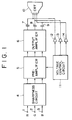
- FIG. 1 there is shown in block diagram an RGB monitor according to a first preferred embodiment of the present invention.
- input terminals 1 to 3 of R, G and B signals are connected to input terminals for R, G and B signals of a sharpness circuit 4a, respectively.
- Output terminals for R, G and B signals of the sharpness circuit 4a are connected to input terminals for R, G and B terminals of a preamplifier 5, respectively.
- Output terminals for R, G and B signals of the preamplifier 5 are connected to input terminals for R, G and B signals of an output amplifier 6, respectively.
- Output terminals for R, G and B signals of the output amplifier 6 are connected to cathodes (not shown) for R, G and B of a cathode ray tube (CRT) 10 through capacitors 7 to 9, respectively.
- a voltage control circuit 11 is connected to the preamplifier 5 and connected also to the cathodes for R, G and B of the CRT 10 through amplifiers 12 to 14, respectively.
- R, G and B signals are supplied to the input terminals 1 to 3, respectively. Further, though not shown, a horizontal synchronizing signal and a vertical synchronizing signal, or a composite synchronizing signal, is supplied to the RGB monitor.
- the R, G and B signals from the input terminals 1 to 3 are supplied to the sharpness circuit 4a.
- the sharpness circuit 4a performs contour correction for all of the R, G and B signals based on a signal detected in accordance with a predetermined condition from among the R, G and B signals. A detailed construction of the sharpness circuit 4a will be hereinafter described.
- the R, G and B signals contour corrected by the sharpness circuit 4a are supplied to the preamplifier 5.
- the preamplifier 5 performs signal processing of the R, G and B signals supplied thereto under the control of the voltage control circuit 11 to adjust the contrast, the black level and so forth of them.
- the R, G and B signals processed by the preamplifier 5 are supplied to the output amplifier 6, and the cathodes of the CRT 10 are driven by R, G and B signals outputted from the output amplifier 6 through the capacitors 7 to 9, respectively.
- the cutoff levels are adjusted in accordance with control signals supplied thereto from the voltage control circuit 11 through the amplifiers 12 to 14.
- the sharpness circuit 4a employed in the RGB monitor detects that one of inputted R, G and B signals which has the smallest amplitude, and performs contour correction of the R, G and B signals based on the detected signal.
- FIG. 2 shows in block diagram an example of a construction of the sharpness circuit 4a employed in the RGB monitor of FIG. 1.
- the sharpness circuit 4a employed in the RGB monitor of FIG. 1 includes a lowest value detection circuit 15, a differentiation circuit 16, a slice circuit 17 and addition circuits 18 to 20.
- the input terminals 1 to 3 are connected to input terminals for R, G and B signals of the lowest value detection circuit 15 and each connected to one of a pair of input terminals of a corresponding one of the addition circuits 18 to 20.
- An output terminal of the lowest value detection circuit 15 is connected to an input terminal of the differentiation circuit 16, and an output terminal of the differentiation circuit 16 is connected to an input terminal of the slice circuit 17.
- An output terminal of the slice circuit 17 is connected to the other input terminals of the addition circuits 18 to 20.
- Output terminals of the addition circuits 18 to 20 are connected to input terminals (not shown) for R, G and B signals of the preamplifier 5, respectively.
- FIG. 3 illustrates in time chart operation of the sharpness circuit 4a.
- R, G and B signals from the input terminals 1 to 3 are supplied to the lowest value detection circuit 15 and also to the addition circuits 18 to 20, respectively.
- the lowest value detection circuit 15 detects, from among the R, G and B signals supplied thereto, a signal which has the smallest amplitude, and outputs the signal as a lowest value signal S1.
- This lowest value signal S1 is near to a brightness signal of a television signal.
- the lowest value detection circuit 15 is constructed so that it can detect, from within any input signals which vary momentarily, an input signal of the smallest amplitude momentarily. Where such R, G and B signals as seen in FIG. 3 are received, the B signal which has the smallest amplitude from among the R, G and B signals is outputted as the lowest value signal S1.
- the lowest value signal S1 from the lowest value detection circuit 15 is supplied to the differentiation circuit 16.
- the differentiation circuit 16 differentiates the lowest value signal S1 to produce a differentiation signal S2.
- This differentiation signal S2 corresponds to an edge component of the lowest value signal S1.
- the differentiation signal S2 from the differentiation circuit 16 is supplied to the addition circuits 18 to 20 through the slice circuit 17.
- a component of the differentiation signal S2 which corresponds to a portion at which a change from black to white occurs is sliced with an arbitrary amplitude by the slice circuit 17.
- the differentiation signal S2' after slice processed by the slice circuit 17 is supplied as a contour correction signal to the addition circuits 18 to 20.
- the addition circuits 18 to 20 add, to the original R, G and B signals from the input terminals 1 to 3 supplied to the first terminals thereof, the differentiation signal S2' from the slice circuit 17 supplied to the second input terminals thereof. Consequently, contour corrected R, G and B signals having a desired sharpness characteristic are produced.
- the contour corrected R, G and B signals are supplied from the output terminals of the addition circuits 18 to 20 to the input terminals for R, G and B signals of the preamplifier 5, respectively, and signal processed by the preamplifier 5, and then supplied to the output amplifier 6. Then, the cathodes of the CRT 10 are driven by the contour corrected R, G and B signals.
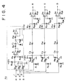
- FIG. 4 shows in circuit diagram an exemplary detailed construction of the sharpness circuit 4a of FIG. 2.
- the input terminals 1 to 3 are connected to the bases of transistors Q 1 to Q 3 and also to the bases of transistors Q 4 to Q 6 , respectively. Further, the input terminals 1 to 3 are grounded through resistors R 1 to R 3 , respectively.
- the collectors and the emitters of the transistors Q 1 to Q 3 are individually connected commonly.
- the commonly connected collectors of the transistors Q 1 to Q 3 are grounded, and the commonly connected emitters are connected to a power supply (not shown), which supplies a power supply voltage of +12 V, through a resistor R 4 .
- the lowest value detection circuit 15 in FIG. 2 is formed from the transistors Q 1 to Q 3 .
- the commonly connected emitters of the transistors Q 1 to Q 3 which form the lowest value detection circuit 15 are connected to a non-negated input terminal of an operational amplifier A 1 , which acts as an amplifier, through a resistor R 5 .
- An output terminal of the operational amplifier A 1 is connected to a negated input terminal of the operational amplifier A 1 through a resistor R 6 , and a junction between the resistor R 6 and the negated input terminal of the operational amplifier A 1 is grounded through a resistor R 7 .
- An output terminal of the operational amplifier A 1 is connected to a terminal of a capacitor C 1 through a resistor R 8 .
- the other terminal of the capacitor C 1 is grounded through a resistor R 9 .
- the capacitor C 1 and the resistor R 9 form a CR resonance circuit, and the differentiation circuit 16 in FIG. 2 is formed from the CR resonance circuit.
- the time constant of the CR resonance circuit formed from the capacitor C 1 and the resistor R 9 can be varied when necessary.
- a diode D 1 is connected at the cathode terminal thereof to a junction between the capacitor C 1 and the resistor R 9 , and the anode terminal of the diode D 1 is grounded.
- the slice circuit 17 in FIG. 2 is formed from the diode D 1 .
- the common junction of the capacitor C 1 , the resistor R 9 and the cathode terminal of the diode D 1 is connected to a non-negated input terminal of an operational amplifier A 2 , which acts as a buffer, through a resistor R 10 .
- An output terminal of the operational amplifier A 2 is connected to a negated input terminal of the operational amplifier A 2 and connected to one of a pair of terminals of each of resistors R 11 to R 13 through a capacitor C 2 .
- the other terminals of the resistors R 11 to R 13 are connected to non-negated input terminals of operational amplifiers A3 to A 5 , respectively.
- Transistors Q 4 to Q 6 connected at the bases thereof to the input terminals 1 to 3, respectively, form emitter follower circuits which act as buffers.
- the collectors of the transistors Q 4 to Q 6 are grounded.
- the emitters of the transistors Q 4 to Q 6 are connected to the power supply (not shown) of +12 V through resistors R 14 to R 16 , respectively.
- the emitters of the transistors Q 4 to Q 6 are connected to first terminals of resistors R 17 to R 19 through capacitors C 3 to C 5 , respectively.
- the other or second terminals of the resistors R 17 to R 19 are connected to non-negated input terminals of the operational amplifiers A 3 to A 5 , respectively.
- the addition circuit 18 in FIG. 2 is formed from the operational amplifier A 3 and the resistors R 11 and R 17 .
- the addition circuit 19 in FIG. 2 is formed from the operational amplifier A 4 and the resistors R 12 and R 18 .
- the addition circuit 20 in FIG. 2 is formed from the operational amplifier A 5 and the resistors R 13 and R 19 .
- the common junction of the non-negated input terminal of the operational amplifier A 3 and the resistors R 11 and R 17 is grounded through a resistor R 20 .
- the common junction of the non-negated input terminal of the operational amplifier A 4 and the resistors R 12 and R 18 is grounded through a resistor R 21 .
- the common junction of the non-negated input terminal of the operational amplifier A 5 and the resistors R 13 and R 19 is grounded through a resistor R 22 .
- Output terminals of the operational amplifiers A 3 to A 5 are connected to the non-negated input terminals of the operational amplifiers A 3 to A 5 through resistors R 23 to R 25 , respectively, and the junctions of the resistors R 23 to R 25 and the non-negated input terminals of the operational amplifiers A 3 to A 5 are grounded through resistors R 26 to R 28 , respectively.
- Output terminals of the operational amplifiers A 3 to A 5 are connected to the input terminals for R, G and B signals of the preamplifier 5 not shown.
- the transistors Q 1 to Q 6 for example, a pnp type bipolar transistor is used. Further, for the operational amplifier A 1 to A 5 , an operational amplifier having a sufficiently high radio frequency characteristic is used.
- R, G and B signals from the input terminals 1 to 3 are supplied to the bases of the transistors Q 1 to Q 3 which form the lowest value detection circuit and the bases of the transistors Q 4 to Q 6 which form emitter follower circuits for buffering, respectively.
- a lowest value signal S1 is detected from among the R, G and B signals from the input terminals 1 to 3.
- the lowest value signal S1 is suitably amplified by the operational amplifier A 1 and then supplied to the differentiation circuit formed from the CR resonance circuit of the capacitor C 1 and the resistor R 9 .
- the differentiation circuit By the differentiation circuit, a differentiation signal S2 of the lowest value signal S1 is produced.
- the differentiation signal S2 is subject to predetermined slice processing by the diode D 1 provided at the input portion of the operational amplifier A 1 for buffering in the next stage.
- a differentiation signal S2' after the slice processing has been performed is supplied to the operational amplifier A 2 . From the operational amplifier A 2 , the differentiation signal S2' is buffer outputted. Meanwhile, from the transistors Q 4 to Q 6 which form emitter followers, the R, G and B signals supplied from the input terminals 1 to 3 are buffer outputted, respectively.
- the differentiation signal S2 buffer outputted from the operational amplifier A 2 is resistance added to the R, G and B signals buffer outputted from the transistors Q 4 to Q 6 through the corresponding resistors R 11 to R 13 and R 17 to R 19 , respectively.
- the operational amplifiers A 3 to A 5 in the next stage effect suitable amplification where they have insufficient amplitudes.
- the RGB monitor since it includes the sharpness circuit 4a constructed so as to detect a lowest value signal S1 from among input R, G and B signals and effect contour correction for all of the R, G and B signals based on a differentiation signal S2 obtained by differentiating the lowest value signal S1, the sharpness of a color image displayed on the CRT 10 is improved, and a picture quality higher than that of a television monitor can be obtained when the CRT 10 displays a photograph or moving pictures. Further, since, from any pattern, no coloring phenomenon occurs at an overshoot portion, a picture quality very preferable for the sense of sight can be obtained.
- contour correction of the R, G and B signals using a differentiation signal S2' obtained by slicing a component of the differentiation signal S2 corresponding to a portion at which a change from black to white occurs with an arbitrary amplitude, the amplitude of the overshoot amount at a character displaying portion is limited. Consequently, even for a pattern wherein a character displaying portion is present in a mixed state in a photograph or moving pictures, optimum contour correction of the entire screen can be performed without deteriorating the picture quality of the character displaying portion remarkably.
- the sharpness circuit 4a is constructed so as to perform contour correction of all of R, G and B signals based on a differentiation signal S2 obtained by differentiating a lowest value detection signal S1 detected from among the input R, G and B signals, simplification in circuit construction can be achieved and matching in peeking among the R, G and B signals can be facilitated comparing with an alternative case wherein sharpness circuits are individually provided for R, G and B signals.
- a contour correction signal used for contour correction in a sharpness circuit is a quadratic differentiation signal.
- a sharpness circuit which uses a quadratic differentiation signal is described.
- An RGB monitor according to the second embodiment is constructed in a similar manner, for example, to the RGB monitor according to the first embodiment shown in FIG. 1.
- a sharpness circuit 4b employed in the RGB monitor according to the second embodiment is constructed such that the differentiation circuit formed from the capacitor C 1 and the resistor R 9 in the sharpness circuit 4a shown in FIG. 4 is replaced by a quadratic differentiation circuit which employs a delay circuit.
- FIG. 5 is a circuit diagram showing an example of the sharpness circuit 4b employed in the RGB monitor according to the present second embodiment.
- an output terminal of an operational amplifier A 1 is connected to a non-negated input terminal of an operational amplifier A 6 which acts as a buffer, and is connected to an input terminal of a delay circuit DL 1 through a resistor R 29 .
- An output terminal of the delay circuit DL 1 is connected to a negated input terminal of an operational amplifier A 7 for reversal through a resistor R 30 , and is connected also to a non-negated input terminal of an operational amplifier A 8 for buffering through another delay circuit DL 2 .
- Outputs of the operational amplifiers A 6 and A 8 are connected to negated input terminals of the operational amplifiers A 6 and A 8 , respectively.
- a output terminal of the operational amplifier A 7 is connected to a non-negated input terminal of the operational amplifier A 7 through a resistor R 31 , and a non-negated input terminal of the operational amplifier A 7 is grounded through a resistor R 32 .
- delay circuits DL 1 and DL 2 delay circuits having an equal delay time are used.
- Output terminals of the operational amplifiers A 6 to A 8 are connected to a negated input terminal of an operational amplifier A 9 for reversal.
- An output terminal of the operational amplifier A 9 is connected to a negated input terminal of the operational amplifier A 9 .
- a non-negated input terminal of the operational amplifier A 9 is grounded through a resistor R 37 .
- An output terminal of the operational amplifier A 9 is connected to non-negated input terminals of the operational amplifiers A 3 to A 5 through the resistors R 11 to R 13 for addition.
- the emitters of the transistors Q 4 to Q 6 are connected to input terminals of delay circuits DL 3 to DL 5 through capacitors C 3 to C 5 , respectively.
- Output terminals of the delay circuits DL 3 to DL 5 are connected to non-negated input terminals of the operational amplifiers A 3 to A 5 through the resistors R 17 to R 19 for addition, respectively.
- delay circuits DL 3 to DL 5 delay circuits having a delay time equal to those of the delay circuits DL 1 and DL 2 are used.
- the remaining part of the sharpness circuit 4b is constructed in a similar manner as in the sharpness circuit 4a shown in FIG. 4.
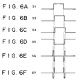
- FIG. 6 is a time chart for explaining operation of the sharpness circuit 4b shown in FIG. 5.
- the waveform A illustrates the lowest value signal S1 at the output terminal of the operational amplifier A 1 ;
- the waveform B illustrates a signal S3 at the output terminal of the delay circuit DL 1 ;
- the waveform C illustrates a signal S4 at the output terminal of the delay circuit DL 2 ;
- the waveform D illustrates a signal S5 at the output terminal of the operational amplifier A 7 ;
- the waveform E illustrates a signal S6 at the common junction of the resistors R 33 to R 35 ;
- the waveform F illustrates a signal (quadratic differentiation signal) S7 at the output terminal of the operational amplifier A 9 .
- the sharpness circuit 4b from the lowest value detection circuit formed from the transistors Q 1 to Q 3 , such a lowest value signal S1 as seen from the waveform A is outputted through the operational amplifier A 1 .
- the lowest value signal S1 is supplied to the operational amplifier A 6 for buffering and supplied also to the delay circuit DL 1 through the resistor R 29 .
- the delay circuit DL 1 produces a signal S3 delayed by a time t from the lowest value signal S1 as seen from the waveform B.
- the signal S3 from the delay circuit DL 1 is supplied to the operational amplifier A 7 for reversal through the resistor R 30 and is supplied to the delay circuit DL 2 .
- the delay circuit DL 2 produces a signal S4 delayed by the time t from the signal S3 as seen from the waveform C.
- the signal S4 from the delay circuit DL 2 is supplied to the operational amplifier A 8 for buffering.
- the lowest value signal S1 from the operational amplifier A 1 is buffer outputted.
- a signal S5 obtained by reversing the signal S3 from the delay circuit DL 1 as seen from the waveform D is outputted.
- the signal S4 from the delay circuit DL 2 is buffer outputted.
- the lowest value signal S1 and the signals S5 and S4 are added through the resistors R 33 to R 35 , respectively. Consequently, such a signal S6 as seen from the waveform E is produced. This signal S6 is supplied to the operational amplifier A 9 .
- the quadratic differentiation signal S7 outputted from the operational amplifier A 9 is resistance added through the corresponding resistors R 11 to R 13 and R 17 to R 19 to the R, G and B signals buffer outputted through the delay circuits DL 3 to DL 5 from the transistors Q 4 to Q 6 which form emitter circuits, respectively. Description of the other operation is omitted here since it is similar to that of the sharpness circuit 4a employed in the RGB monitor according to the first embodiment. According to the second embodiment, similar effects to those of the first embodiment can be obtained.
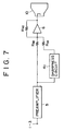
- FIG. 7 is a block diagram showing an example of a construction of an RGB monitor according to the third embodiment.
- input terminals 1 to 3 for R, G and B signals are connected to input terminals of a preamplifier 5.
- Output terminals of the preamplifier 5 are connected to input terminals of an output amplifier 6 through resistors R 38 and connected to input terminals of a sharpness circuit 4c.
- Output terminals of the sharpness circuit 4c are connected to input terminals of the output amplifier 6 through resistors R 39 .
- Output terminals of the output amplifier 6 are connected to input terminals of the output amplifier 6 through resistors R 40 and connected to cathodes of a CRT 10.
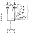
- FIG. 8 is a circuit diagram showing an exemplary detailed construction of the sharpness circuit 4c employed in the RGB monitor shown in FIG. 7.
- the output terminals for R, G and B signals of the preamplifier 5 are connected to the input terminals for R, G and B signals of the sharpness circuit 4c and connected to the input terminals of the output amplifier 6 for R, G and B signals through the resistors R 38 , respectively.
- the sharpness circuit 4c is constructed in a similar manner to that portion surrounded by a broken line in FIG. 4 of the first embodiment, that is, a portion which forms the lowest value detection circuit, differentiation circuit and slice circuit.
- the bases of the transistors Q 1 to Q 3 which form the lowest value detection circuit are connected to the output terminals for R, G and B signals of the preamplifier 5, respectively.
- the operational amplifier A 1 for amplification in FIG. 4 is replaced by the transistor Q 7 which forms an emitter follower circuit.
- an npn type bipolar transistor may be used.
- the collector of the transistor Q 7 is connected to a power supply of +12 V.
- the emitter of the transistor Q 7 is grounded through a resistor R 41 and is connected to the capacitor C 1 which forms the differentiation circuit through the resistor R 8 .
- An output terminal of the operational amplifier A 2 for buffering of the sharpness circuit 4c is connected to the input terminals of the output amplifier 6 for R, G and B signals through the resistors R 39 .
- the remaining part of the RGM monitor is constructed in a similar manner as in the RGB monitor according to the first embodiment. It is to be noted that, in FIG. 7, the capacitors 7 to 9, voltage control circuit 11 and amplifiers 12 to 14 are omitted. Further, while, in FIG. 7, signal paths are indicated by a single path for simplification, signal paths are actually provided individually for R, G and B signals similarly as in FIG. 1.
- the sharpness circuit 4c is provided at the following stage to the preamplifier 5 and the output amplifier 6 is formed as of the feedback amplification type, and a contour correction signal from the sharpness circuit 4c is added to R, G and B signals from the preamplifier 5 at the input stage of the output amplifier 6.
- the R, G and B signals from the preamplifier 5 are supplied to the sharpness circuit 4c and also to the output amplifier 6 for R, G and B signals.
- the sharpness circuit 4c detects a lowest value signal S1 from among the R, G and B signals supplied thereto from the preamplifier 5 and produces a differentiation signal S2' corresponding to an edge portion of the lowest value signal S1. Then, the differentiation signal S2' is supplied as a contour correction signal to the output amplifier 6 for R, G and B signals.
- the differentiation signal S2' supplied from the sharpness circuit 4c is resistance added to the R, G and B signals supplied from the preamplifier 5 through respective corresponding ones of the resistors R 38 and R 39 so that R, G and B signals having a desired sharpness characteristic are produced.
- Description of the other operation is omitted since it is similar to that of the first embodiment. According to the present third embodiment, similar effects to those of the first embodiment can be obtained.
- FIG. 9 is a block diagram showing an example of a construction of an RGB monitor according to the fourth embodiment.
- input terminals 1 to 3 are connected to input terminals of the preamplifier 5.
- Output terminals of the preamplifier 5 are connected to input terminals of an output amplifier 6 and also to input terminals of a sharpness circuit 4d.
- Output terminals of the sharpness circuit 4d are connected to a first grid electrode G1 of a CRT 10 through an amplifier 21.
- FIG. 10 is a circuit diagram showing an exemplary detailed construction of the sharpness circuit 4d employed in the RGB monitor shown in FIG. 9.
- the present sharpness circuit 4d is constructed in a similar manner to the sharpness circuit 4c shown in FIG. 8.
- an output terminal of the sharpness circuit 4d that is, a common junction of a capacitor C 1 and a resistor R 9 which form a differentiation circuit and a diode D 1 which forms a slice circuit, is connected to an input terminal of the amplifier 21.
- an amplifier similar to the amplifiers (not shown) for R, G and B signals used for the output amplifier 6 is used.
- An output terminal of the amplifier 21 is connected to the first grid electrode G1 of the CRT 10 through a capacitor 22.
- a bias power supply 23 for the first grid electrode G1 is connected at the negative pole thereof to the first grid electrode G1 through a resistor R 42 , while the positive pole of the bias power supply 23 is grounded.
- the remaining part of the RGB monitor of the fourth embodiment is constructed in a similar manner to the RGB monitor according to the first embodiment. It is to be noted that, in FIG. 9, the capacitors 7 to 9, voltage control circuit 11 and amplifiers 12 to 14 are omitted. Further, while, in FIG. 9, signal paths are indicated by a single path for simplification, signal paths are actually provided individually for R, G and B signals similarly as in FIG. 1.
- the sharpness circuit 4d is provided at the stage following the preamplifier 5 and a contour correction signal (differentiation signal S2') from the sharpness circuit 4d is added to the bias to the first grid electrode G1 of the CRT 10 to effect contour correction of R, G and B signals for driving the cathodes of the CRT 10.
- FIG. 11 is a block diagram showing an exemplary detailed construction of the sharpness circuit 4e which is employed in the RGB monitor according to the fifth embodiment.
- the present sharpness circuit 4e includes, in addition to a construction similar to that of the sharpness circuit 4a of the first embodiment, a highest value detection circuit 24 and a calculation circuit 25. Further, the slice circuit 17 in FIG. 2 is replaced by a non-linear amplification circuit 26, and the addition circuits 18 to 20 in FIG. 2 are replaced by addition/subtraction circuits 27 to 29, respectively.
- input terminals for R, G and B signals of the highest value detection circuit 24 are connected to the input terminals 1 to 3, respectively. Meanwhile, output terminals of the lowest value detection circuit 15 and the highest value detection circuit 24 are connected to input terminals of the calculation circuit 25, and an output terminal of the calculation circuit 25 is connected to an input terminal of the differentiation circuit 16.
- the highest value detection circuit 24 detects, from among R, G and B signals supplied thereto from the input terminals 1 to 3, a signal having the largest amplitude, and outputs the signal as a highest value signal S8.
- the calculation circuit 25 calculates, for example, when the lowest value signal S1 from the lowest value detection circuit 15 and the highest value signal S8 from the highest value detection circuit 24 are different in amplitude from each other, the sum of or the difference between them.
- the non-linear amplification circuit 26 connected to the differentiation circuit 16 effects such non-linear amplification that, for example, the amplification factor is decreased in a region wherein the amplitude of the differentiation signal S2 from the differentiation circuit 16 is larger, but the amplification factor is increased in another region wherein the amplification factor of the differentiation signal S2 is smaller.
- the addition/subtraction circuits 27 to 29 effect addition or subtraction of a differentiation signal S2'' supplied thereto from the differentiation circuit 16 through the non-linear amplification circuit 26 to or from the R, G and B signals supplied thereto from the input terminals 1 to 3. Consequently, it is possible not only to emphasize a contour provided by the R, G and B signals but also to make a contour provided by the R, G and B signals dull conversely. Description of the remaining part of the RGB monitor is omitted here because it is similar as in the first embodiment. Also by the fifth embodiment, similar effects to those of the first embodiment can be obtained.
- the sharpness circuits 4a to 4e on/off or another function of setting the amount of sharpness to an arbitrary value.
- contour correction in a vertical direction may be performed alternatively.
- a differentiation signal for contour correction in a vertical direction can be formed by modifying the second embodiment described above such that the delay time t of the delay circuits DL 1 to DL 5 of the sharpness circuit 4b is set to 1 horizontal period.
Landscapes
- Engineering & Computer Science (AREA)
- Multimedia (AREA)
- Signal Processing (AREA)
- Processing Of Color Television Signals (AREA)
- Picture Signal Circuits (AREA)
Abstract
Description
Claims (12)
- An aperture compensation circuit (4) comprising:detection means (15) for detecting a particular signal from among an R signal, a G signal and a B signal supplied thereto;differentiation means (16) for producing a differentiation signal of the particular signal; andaddition means (18,19,20) for adding the differentiation signal to the R signal, the G signal and the B signal.
- An aperture compensation circuit according to claim 1, wherein the particular signal is that one of the R signal, the G signal and the B signal which has the smallest amplitude.
- An aperture compensation circuit according to claim 1, wherein the particular signal is that one of the R signal, the G signal and the B signal which has the largest amplitude.
- An aperture compensation circuit according to claim 1, wherein the particular signal is the G signal.
- An aperture compensation circuit according to any one of the preceding claims, wherein said differentiation means (16) performs quadratic differentiation of the particular signal.
- An aperture compensation circuit according to any one of the preceding claims, further comprising calculation means (25) provided between said detection means (15,24) and said differentiation means (16) for performing some calculation to produce the particular signal.
- An aperture compensation circuit according to any of the preceding claims, further comprising slice means (17) provided between said differentiation means (16) and said addition means (18,19,20) for slicing the differentiation signal with a particular amplitude.
- An aperture compensation circuit according to any one of the preceding claims, further comprising non-linear amplification means (26) provided between said differentiation means (16) and said addition means (27,28,29) for non-linearly amplifying the differentiation signal.
- An aperture compensation circuit according to any one of the preceding claims, further comprising amplitude control means for controlling the amplitude of the differentiation signal.
- An RGB monitor to which an R signal, a G signal and a B signal are inputted, comprising:detection means (15) for detecting a particular signal from among an R signal, a G signal and a B signal inputted to said RGM monitor;differentiation means (16) for producing a differentiation signal of the particular signal;addition means (18,19,20) for adding the differentiation signal to the R signal, the G signal and the B signal to effect contour correction; anda CRT (10) connected to be driven by the R signal, G signal and B signal for which the contour correction has been performed.
- An RGB monitor according to claim 10, wherein the particular signal is that one of the R signal, the G signal and the B signal which has the smallest amplitude.
- An RGB monitor according to claim 10 or 11, wherein the RGB monitor is arranged to use the differentiation signal as a bias signal to a first grid electrode of said CRT (10) so that, when said CRT (10) is to be driven, contour correction of the R signal, G signal and B signal for driving said CRT (10) is performed.
Applications Claiming Priority (3)
| Application Number | Priority Date | Filing Date | Title |
|---|---|---|---|
| JP29111196 | 1996-10-14 | ||
| JP8291111A JPH10116050A (en) | 1996-10-14 | 1996-10-14 | Contour correction circuit and rgb monitor |
| JP291111/96 | 1996-10-14 |
Publications (2)
| Publication Number | Publication Date |
|---|---|
| EP0836331A2 true EP0836331A2 (en) | 1998-04-15 |
| EP0836331A3 EP0836331A3 (en) | 2000-07-12 |
Family
ID=17764604
Family Applications (1)
| Application Number | Title | Priority Date | Filing Date |
|---|---|---|---|
| EP97308085A Withdrawn EP0836331A3 (en) | 1996-10-14 | 1997-10-13 | Aperture compensation circuit and RGB monitor |
Country Status (6)
| Country | Link |
|---|---|
| US (1) | US5926058A (en) |
| EP (1) | EP0836331A3 (en) |
| JP (1) | JPH10116050A (en) |
| KR (1) | KR19980032647A (en) |
| SG (1) | SG66402A1 (en) |
| TW (1) | TW358318B (en) |
Cited By (1)
| Publication number | Priority date | Publication date | Assignee | Title |
|---|---|---|---|---|
| CN111787298A (en) * | 2020-07-14 | 2020-10-16 | 深圳创维-Rgb电子有限公司 | Image quality compensation method, device and terminal device for liquid crystal display device |
Families Citing this family (2)
| Publication number | Priority date | Publication date | Assignee | Title |
|---|---|---|---|---|
| JP3937426B2 (en) * | 2001-07-16 | 2007-06-27 | 日本電気株式会社 | Preamplifier circuit |
| KR20040019213A (en) * | 2002-08-27 | 2004-03-05 | 이미지퀘스트(주) | Visual signal control circuit with sharpness compensation circuit |
Family Cites Families (14)
| Publication number | Priority date | Publication date | Assignee | Title |
|---|---|---|---|---|
| FR2583244B1 (en) * | 1985-06-05 | 1987-08-07 | Thomson Video Equip | DEVICE FOR CORRECTING CONTOURS IN AN IMAGE AND USE OF SUCH A DEVICE IN A COLOR TELEVISION CAMERA |
| JPS62239670A (en) * | 1986-04-11 | 1987-10-20 | Ikegami Tsushinki Co Ltd | Contour emphasizing device |
| JPS6418374A (en) * | 1987-07-14 | 1989-01-23 | Sharp Kk | Contour correcting method for television video |
| JPH02280465A (en) * | 1989-04-20 | 1990-11-16 | Sanyo Electric Co Ltd | Picture quality improvement circuit for crt |
| KR920007040Y1 (en) * | 1989-09-19 | 1992-09-28 | 안영남 | Electrical power control device for industry |
| GB9001429D0 (en) * | 1990-01-22 | 1990-03-21 | British Broadcasting Corp | Improvements in television |
| JPH04100487A (en) * | 1990-08-20 | 1992-04-02 | Ikegami Tsushinki Co Ltd | Contour correction method |
| DE69223679T2 (en) * | 1991-05-16 | 1998-04-30 | Victor Company Of Japan | Image quality improvement circuit for image contour compensation |
| JPH05244414A (en) * | 1992-02-28 | 1993-09-21 | Canon Inc | Picture processor |
| US5298981A (en) * | 1992-10-22 | 1994-03-29 | Panasonic Technologies, Inc. | Color signal aperture correction system having automatically selected source signal |
| JPH07162890A (en) * | 1993-12-08 | 1995-06-23 | Matsushita Electric Ind Co Ltd | White balance adjustment device |
| KR960007544B1 (en) * | 1993-09-10 | 1996-06-05 | 삼성전자 주식회사 | On-Screen Display on Monitors |
| DE59406405D1 (en) * | 1993-09-17 | 1998-08-13 | De La Rue Giori Sa | Printing unit for a web printing machine |
| US5751451A (en) * | 1995-05-26 | 1998-05-12 | Minolta Co., Ltd. | Film image reading system |
-
1996
- 1996-10-14 JP JP8291111A patent/JPH10116050A/en active Pending
-
1997
- 1997-10-07 US US08/944,962 patent/US5926058A/en not_active Expired - Fee Related
- 1997-10-07 TW TW086114685A patent/TW358318B/en active
- 1997-10-08 KR KR1019970051559A patent/KR19980032647A/en not_active Ceased
- 1997-10-10 SG SG1997003721A patent/SG66402A1/en unknown
- 1997-10-13 EP EP97308085A patent/EP0836331A3/en not_active Withdrawn
Cited By (2)
| Publication number | Priority date | Publication date | Assignee | Title |
|---|---|---|---|---|
| CN111787298A (en) * | 2020-07-14 | 2020-10-16 | 深圳创维-Rgb电子有限公司 | Image quality compensation method, device and terminal device for liquid crystal display device |
| US11776498B2 (en) | 2020-07-14 | 2023-10-03 | Shenzhen Chuangwei-Rgb Electronics Co., Ltd. | Image quality compensation method for liquid crystal display device, device and terminal equipment |
Also Published As
| Publication number | Publication date |
|---|---|
| SG66402A1 (en) | 1999-07-20 |
| KR19980032647A (en) | 1998-07-25 |
| TW358318B (en) | 1999-05-11 |
| US5926058A (en) | 1999-07-20 |
| EP0836331A3 (en) | 2000-07-12 |
| JPH10116050A (en) | 1998-05-06 |
| MX9707874A (en) | 1998-06-30 |
Similar Documents
| Publication | Publication Date | Title |
|---|---|---|
| EP1858257B1 (en) | Display device, contrast adjusting method and contrast adjusting program | |
| KR100691553B1 (en) | Image signal processing circuit and television receiver | |
| US5699127A (en) | Automatic brightness limiter automatic control circuit, contrast limiter control circuit, luminance/color difference signal processor and video display apparatus | |
| US20030156225A1 (en) | Gradation correction apparatus | |
| EP0218456B1 (en) | Automatic bias control of an image display device in a video monitor | |
| US5926058A (en) | Aperture compensation circuit and RGB monitor | |
| US4679092A (en) | Reduced distortion display circuit | |
| JPH0353832B2 (en) | ||
| US4689679A (en) | Brightness and automatic kinescope bias control in a video signal processor with an AC coupled kinescope driver | |
| US6577285B1 (en) | Gamma corrector and image display device using the same | |
| US5726540A (en) | Transient enhancement circuit for CRT amplifier | |
| US4730210A (en) | Wideband analog RGB video processor with negative feedback capability and black level control | |
| US6541927B2 (en) | Color cathode ray tube and adjusting method | |
| US4979044A (en) | Automatic contrast circuit for instantaneous compensation | |
| JP3237207B2 (en) | Color video display device and video signal processing circuit | |
| JP2938264B2 (en) | Liquid crystal display | |
| US20040196271A1 (en) | Method for controlling video signal circuit, display device and computer | |
| KR980013287A (en) | Luminance signal gamma correction device in video equipment | |
| US5757340A (en) | Amplifier with a second active element being cascode connected to a first active element and having a control electrode connected to a constant voltage | |
| MXPA97007874A (en) | Opening and monitor compensation circuit | |
| KR20010076333A (en) | Gamma correction circuit for imaging signal and display apparatus including such gamma correction circuit | |
| JPH10191102A (en) | Video signal amplifier circuit | |
| KR20000009203U (en) | Monitor back raster adjustment circuit | |
| KR100447188B1 (en) | Gamma Correction Device of display device | |
| JPH0865698A (en) | Video display |
Legal Events
| Date | Code | Title | Description |
|---|---|---|---|
| PUAI | Public reference made under article 153(3) epc to a published international application that has entered the european phase |
Free format text: ORIGINAL CODE: 0009012 |
|
| AK | Designated contracting states |
Kind code of ref document: A2 Designated state(s): DE FR GB |
|
| AX | Request for extension of the european patent |
Free format text: AL;LT;LV;RO;SI |
|
| PUAL | Search report despatched |
Free format text: ORIGINAL CODE: 0009013 |
|
| AK | Designated contracting states |
Kind code of ref document: A3 Designated state(s): AT BE CH DE DK ES FI FR GB GR IE IT LI LU MC NL PT SE |
|
| AX | Request for extension of the european patent |
Free format text: AL;LT;LV;RO;SI |
|
| 17P | Request for examination filed |
Effective date: 20001219 |
|
| AKX | Designation fees paid |
Free format text: DE FR GB |
|
| STAA | Information on the status of an ep patent application or granted ep patent |
Free format text: STATUS: THE APPLICATION HAS BEEN WITHDRAWN |
|
| 18W | Application withdrawn |
Withdrawal date: 20020930 |