EP0837622A1 - Plasma generator - Google Patents
Plasma generator Download PDFInfo
- Publication number
- EP0837622A1 EP0837622A1 EP96116612A EP96116612A EP0837622A1 EP 0837622 A1 EP0837622 A1 EP 0837622A1 EP 96116612 A EP96116612 A EP 96116612A EP 96116612 A EP96116612 A EP 96116612A EP 0837622 A1 EP0837622 A1 EP 0837622A1
- Authority
- EP
- European Patent Office
- Prior art keywords
- plasma generator
- discharging
- dielectric
- plasma
- high voltage
- Prior art date
- Legal status (The legal status is an assumption and is not a legal conclusion. Google has not performed a legal analysis and makes no representation as to the accuracy of the status listed.)
- Ceased
Links
- 239000007789 gas Substances 0.000 claims abstract description 29
- 239000007788 liquid Substances 0.000 claims abstract description 16
- 239000000126 substance Substances 0.000 claims abstract description 15
- 239000007787 solid Substances 0.000 claims abstract description 9
- 238000012545 processing Methods 0.000 claims abstract description 8
- 239000004020 conductor Substances 0.000 claims description 19
- 239000004065 semiconductor Substances 0.000 claims description 18
- 239000003990 capacitor Substances 0.000 claims description 10
- 239000000463 material Substances 0.000 claims description 6
- 239000000203 mixture Substances 0.000 claims description 5
- 230000008878 coupling Effects 0.000 claims description 4
- 238000010168 coupling process Methods 0.000 claims description 4
- 238000005859 coupling reaction Methods 0.000 claims description 4
- 230000010355 oscillation Effects 0.000 claims description 4
- 238000007599 discharging Methods 0.000 claims 12
- 230000001131 transforming effect Effects 0.000 claims 2
- 230000004913 activation Effects 0.000 abstract description 13
- 239000003814 drug Substances 0.000 abstract description 4
- 238000002560 therapeutic procedure Methods 0.000 abstract description 4
- 230000003247 decreasing effect Effects 0.000 abstract description 3
- 238000001994 activation Methods 0.000 abstract description 2
- 230000005495 cold plasma Effects 0.000 abstract description 2
- 238000005516 engineering process Methods 0.000 abstract description 2
- 238000000746 purification Methods 0.000 abstract description 2
- 238000011084 recovery Methods 0.000 abstract description 2
- 208000028659 discharge Diseases 0.000 description 35
- 238000000034 method Methods 0.000 description 20
- 230000008569 process Effects 0.000 description 19
- 238000004804 winding Methods 0.000 description 14
- 238000010586 diagram Methods 0.000 description 13
- 230000006698 induction Effects 0.000 description 12
- 239000002245 particle Substances 0.000 description 11
- 230000006870 function Effects 0.000 description 10
- 229910052751 metal Inorganic materials 0.000 description 10
- 239000002184 metal Substances 0.000 description 10
- 230000005284 excitation Effects 0.000 description 9
- 239000012530 fluid Substances 0.000 description 7
- 239000000443 aerosol Substances 0.000 description 6
- 230000003287 optical effect Effects 0.000 description 5
- 238000012546 transfer Methods 0.000 description 5
- XKRFYHLGVUSROY-UHFFFAOYSA-N Argon Chemical compound [Ar] XKRFYHLGVUSROY-UHFFFAOYSA-N 0.000 description 4
- 239000013078 crystal Substances 0.000 description 4
- 239000011521 glass Substances 0.000 description 4
- 238000006467 substitution reaction Methods 0.000 description 4
- 238000013461 design Methods 0.000 description 3
- 239000006185 dispersion Substances 0.000 description 3
- -1 for instance Substances 0.000 description 3
- 238000010438 heat treatment Methods 0.000 description 3
- 230000001939 inductive effect Effects 0.000 description 3
- 230000007935 neutral effect Effects 0.000 description 3
- 239000010453 quartz Substances 0.000 description 3
- VYPSYNLAJGMNEJ-UHFFFAOYSA-N silicon dioxide Inorganic materials O=[Si]=O VYPSYNLAJGMNEJ-UHFFFAOYSA-N 0.000 description 3
- XLYOFNOQVPJJNP-UHFFFAOYSA-N water Substances O XLYOFNOQVPJJNP-UHFFFAOYSA-N 0.000 description 3
- 229910000859 α-Fe Inorganic materials 0.000 description 3
- 229910000906 Bronze Inorganic materials 0.000 description 2
- 230000005668 Josephson effect Effects 0.000 description 2
- XUIMIQQOPSSXEZ-UHFFFAOYSA-N Silicon Chemical compound [Si] XUIMIQQOPSSXEZ-UHFFFAOYSA-N 0.000 description 2
- 229910052786 argon Inorganic materials 0.000 description 2
- 230000000712 assembly Effects 0.000 description 2
- 238000000429 assembly Methods 0.000 description 2
- 239000010974 bronze Substances 0.000 description 2
- 238000006243 chemical reaction Methods 0.000 description 2
- KUNSUQLRTQLHQQ-UHFFFAOYSA-N copper tin Chemical compound [Cu].[Sn] KUNSUQLRTQLHQQ-UHFFFAOYSA-N 0.000 description 2
- 125000004122 cyclic group Chemical group 0.000 description 2
- 208000037265 diseases, disorders, signs and symptoms Diseases 0.000 description 2
- 230000005672 electromagnetic field Effects 0.000 description 2
- 230000005674 electromagnetic induction Effects 0.000 description 2
- PCHJSUWPFVWCPO-UHFFFAOYSA-N gold Chemical compound [Au] PCHJSUWPFVWCPO-UHFFFAOYSA-N 0.000 description 2
- 239000010931 gold Substances 0.000 description 2
- 229910052737 gold Inorganic materials 0.000 description 2
- 239000001307 helium Substances 0.000 description 2
- 229910052734 helium Inorganic materials 0.000 description 2
- SWQJXJOGLNCZEY-UHFFFAOYSA-N helium atom Chemical compound [He] SWQJXJOGLNCZEY-UHFFFAOYSA-N 0.000 description 2
- 238000004020 luminiscence type Methods 0.000 description 2
- 229910052754 neon Inorganic materials 0.000 description 2
- GKAOGPIIYCISHV-UHFFFAOYSA-N neon atom Chemical compound [Ne] GKAOGPIIYCISHV-UHFFFAOYSA-N 0.000 description 2
- 238000007747 plating Methods 0.000 description 2
- 230000010287 polarization Effects 0.000 description 2
- 239000000843 powder Substances 0.000 description 2
- 239000000523 sample Substances 0.000 description 2
- 229910052710 silicon Inorganic materials 0.000 description 2
- 239000010703 silicon Substances 0.000 description 2
- 230000005418 spin wave Effects 0.000 description 2
- 230000009466 transformation Effects 0.000 description 2
- 230000001052 transient effect Effects 0.000 description 2
- 230000007704 transition Effects 0.000 description 2
- 230000005641 tunneling Effects 0.000 description 2
- 235000012431 wafers Nutrition 0.000 description 2
- OKTJSMMVPCPJKN-UHFFFAOYSA-N Carbon Chemical compound [C] OKTJSMMVPCPJKN-UHFFFAOYSA-N 0.000 description 1
- RYGMFSIKBFXOCR-UHFFFAOYSA-N Copper Chemical compound [Cu] RYGMFSIKBFXOCR-UHFFFAOYSA-N 0.000 description 1
- 239000004593 Epoxy Substances 0.000 description 1
- ZOKXTWBITQBERF-UHFFFAOYSA-N Molybdenum Chemical compound [Mo] ZOKXTWBITQBERF-UHFFFAOYSA-N 0.000 description 1
- 229910000831 Steel Inorganic materials 0.000 description 1
- 239000004809 Teflon Substances 0.000 description 1
- 229920006362 Teflon® Polymers 0.000 description 1
- RTAQQCXQSZGOHL-UHFFFAOYSA-N Titanium Chemical compound [Ti] RTAQQCXQSZGOHL-UHFFFAOYSA-N 0.000 description 1
- QCWXUUIWCKQGHC-UHFFFAOYSA-N Zirconium Chemical compound [Zr] QCWXUUIWCKQGHC-UHFFFAOYSA-N 0.000 description 1
- 238000009825 accumulation Methods 0.000 description 1
- 230000009471 action Effects 0.000 description 1
- 229910045601 alloy Inorganic materials 0.000 description 1
- 239000000956 alloy Substances 0.000 description 1
- 230000015572 biosynthetic process Effects 0.000 description 1
- 239000003054 catalyst Substances 0.000 description 1
- 230000000739 chaotic effect Effects 0.000 description 1
- 239000002131 composite material Substances 0.000 description 1
- 150000001875 compounds Chemical class 0.000 description 1
- 238000010276 construction Methods 0.000 description 1
- 229910052802 copper Inorganic materials 0.000 description 1
- 239000010949 copper Substances 0.000 description 1
- 238000012937 correction Methods 0.000 description 1
- 230000001419 dependent effect Effects 0.000 description 1
- 238000011161 development Methods 0.000 description 1
- 201000010099 disease Diseases 0.000 description 1
- 208000035475 disorder Diseases 0.000 description 1
- 239000000428 dust Substances 0.000 description 1
- 230000000694 effects Effects 0.000 description 1
- 238000010891 electric arc Methods 0.000 description 1
- 230000005684 electric field Effects 0.000 description 1
- 230000002349 favourable effect Effects 0.000 description 1
- 239000007888 film coating Substances 0.000 description 1
- 238000009501 film coating Methods 0.000 description 1
- 229920002313 fluoropolymer Polymers 0.000 description 1
- 229910002804 graphite Inorganic materials 0.000 description 1
- 239000010439 graphite Substances 0.000 description 1
- 239000001257 hydrogen Substances 0.000 description 1
- 229910052739 hydrogen Inorganic materials 0.000 description 1
- 125000004435 hydrogen atom Chemical class [H]* 0.000 description 1
- 230000010354 integration Effects 0.000 description 1
- 230000003993 interaction Effects 0.000 description 1
- 230000004807 localization Effects 0.000 description 1
- 230000007246 mechanism Effects 0.000 description 1
- 150000002739 metals Chemical class 0.000 description 1
- 238000012986 modification Methods 0.000 description 1
- 230000004048 modification Effects 0.000 description 1
- 229910052750 molybdenum Inorganic materials 0.000 description 1
- 239000011733 molybdenum Substances 0.000 description 1
- 229910052758 niobium Inorganic materials 0.000 description 1
- 239000010955 niobium Substances 0.000 description 1
- GUCVJGMIXFAOAE-UHFFFAOYSA-N niobium atom Chemical compound [Nb] GUCVJGMIXFAOAE-UHFFFAOYSA-N 0.000 description 1
- 230000007170 pathology Effects 0.000 description 1
- 238000010248 power generation Methods 0.000 description 1
- 230000000630 rising effect Effects 0.000 description 1
- 238000001228 spectrum Methods 0.000 description 1
- 239000010959 steel Substances 0.000 description 1
- 229910052715 tantalum Inorganic materials 0.000 description 1
- GUVRBAGPIYLISA-UHFFFAOYSA-N tantalum atom Chemical compound [Ta] GUVRBAGPIYLISA-UHFFFAOYSA-N 0.000 description 1
- 230000001225 therapeutic effect Effects 0.000 description 1
- 229910052726 zirconium Inorganic materials 0.000 description 1
Images








Classifications
-
- H—ELECTRICITY
- H01—ELECTRIC ELEMENTS
- H01J—ELECTRIC DISCHARGE TUBES OR DISCHARGE LAMPS
- H01J37/00—Discharge tubes with provision for introducing objects or material to be exposed to the discharge, e.g. for the purpose of examination or processing thereof
- H01J37/32—Gas-filled discharge tubes
- H01J37/32009—Arrangements for generation of plasma specially adapted for examination or treatment of objects, e.g. plasma sources
-
- H—ELECTRICITY
- H01—ELECTRIC ELEMENTS
- H01J—ELECTRIC DISCHARGE TUBES OR DISCHARGE LAMPS
- H01J37/00—Discharge tubes with provision for introducing objects or material to be exposed to the discharge, e.g. for the purpose of examination or processing thereof
- H01J37/32—Gas-filled discharge tubes
- H01J37/32009—Arrangements for generation of plasma specially adapted for examination or treatment of objects, e.g. plasma sources
- H01J37/32018—Glow discharge
- H01J37/32045—Circuits specially adapted for controlling the glow discharge
-
- H—ELECTRICITY
- H05—ELECTRIC TECHNIQUES NOT OTHERWISE PROVIDED FOR
- H05H—PLASMA TECHNIQUE; PRODUCTION OF ACCELERATED ELECTRICALLY-CHARGED PARTICLES OR OF NEUTRONS; PRODUCTION OR ACCELERATION OF NEUTRAL MOLECULAR OR ATOMIC BEAMS
- H05H1/00—Generating plasma; Handling plasma
- H05H1/24—Generating plasma
- H05H1/46—Generating plasma using applied electromagnetic fields, e.g. high frequency or microwave energy
-
- H—ELECTRICITY
- H05—ELECTRIC TECHNIQUES NOT OTHERWISE PROVIDED FOR
- H05H—PLASMA TECHNIQUE; PRODUCTION OF ACCELERATED ELECTRICALLY-CHARGED PARTICLES OR OF NEUTRONS; PRODUCTION OR ACCELERATION OF NEUTRAL MOLECULAR OR ATOMIC BEAMS
- H05H2240/00—Testing
- H05H2240/20—Non-thermal plasma
-
- H—ELECTRICITY
- H05—ELECTRIC TECHNIQUES NOT OTHERWISE PROVIDED FOR
- H05H—PLASMA TECHNIQUE; PRODUCTION OF ACCELERATED ELECTRICALLY-CHARGED PARTICLES OR OF NEUTRONS; PRODUCTION OR ACCELERATION OF NEUTRAL MOLECULAR OR ATOMIC BEAMS
- H05H2277/00—Applications of particle accelerators
- H05H2277/10—Medical devices
Definitions
- the present invention relates to a plasma generator, more specifically, to a plasma generator to apply cold plasma in the fields of medicine, biology, ecological recovery, activation, purification, special processing of gases, liquids and solid substances as well as other areas of technology and science.
- Plasmotrons which can generate plasma under normal atmospheric pressure conditions with temperature up to thousands degrees Celsius are well known in the art.
- the thermal heating of plasma is actived by classical electromagnetic induction, via induction heating of electrically conducting media in alternating electromagnetic field of the inductor.
- the device consists of high voltage AC generator, quartz pipe-shaped case and liquid-cooled inductor, an inductance coil having large numbers of turns.
- a multi-turn inductor of 0.1 m diameter is essentially required, the inductor reactance being raised greatly at 1 MHz and higher frequencies.
- the prior art plasmotron has revealed some drawbacks of large dimensions, poor efficiency and very high plasma temperature, which, in turn, restricted its operational features considerably, especially in medicine, biology and ecological treatment.
- the other types of plasma generator have been used in electric discharge therapy device which comprise electronic oscillator, modulation unit, output resonance transformer and rod-like discharge electrode.
- a plasma beam is induced between the end of the electrode and the biological object.
- the electronic oscillator produces oscillations in 200 kHz through 300 kHz frequency range.
- the modulator which can be constructed in transistors periodically switches on and off the signal of the oscillator at about 3 kHz to 5 kHz rate.
- the modulator provides impact excitation of resonance transformer circuit, which brings about measured output emission in a form of corona discharge between the electrode and the object.
- the device produces favorable therapeutic effect to treat a number of diseases, disorders, pathologies, mainly due to the induced heat in the specified areas of body.
- the device has also revealed shortcomings that the discharge transformation from corona to spark form may be appeared and the conduction currents origination directly in the tissue.
- the classical corona and spark discharge inevitably results in ionization, electric break-through and thermal heating of the air gap between the inducing electrode and the body which is used as the second electrode.
- direct resonance action of the device by virtue of field is shunted as a result of ionization of substantial medium and chaotic heat motion of particles in the discharge area.
- a primary object of the invention is, therefore, to provide a universal plasma generator with decreased mass and dimensions which provides unipolar plasma for plasma therapy and activation of substantial media by virtue of the field.
- a plasma generator of the invention comprises:
- FIG. 1 a structural circuit diagram of the plasma generator of the present invention is shown schematically.
- the plasma generator employs a conventional DC power source (7), which consists of AC voltage reducing transformer (8), bridge rectifier (9) and capacitor filter (10).
- the structure of the primary resonance circuit (13) constituting the electronic oscillator (1) involves non-linear capacitor (17) as well as the input low voltage section (14) of the resonance transformer (4).
- the primary resonance circuit (13) also includes an amplifying (control) element (3), e.g., a transistor.
- the plasma generator is optionally equipped with a drive unit (2) which is connected to the amplifying (control) element (3) and provides cyclic switching on and off of the amplifying (control) element (3) or another special drive mode.
- the drive unit (2) can be made with an electronic integrated circuit or diode-resistor assembly.
- the parametric resonance transformer (4) can be realized as an induction multi-turn coil transformer. In many cases, it makes sense to furnish the resonance transformer (4) with ferrite core (22). Feedback section (23) of the resonance transformer (4) is connected to control input (27) of the amplifying (control) element (3). A junction capacitor (26), correction resistors (28, 29) and diode (30) can be used for optimal operational conditions.
- the high voltage output section (31) of the resonance transformer (4) that is the secondary multilayer winding, is placed directly at the ferrite core (22). This high voltage output section (31) consists of inductive layers (32, 33, 34 and so on), whose number can be 10 to 20.
- the layer capacitance (35, 36, 37) which forms a cell (38) of transfer line in conjunction with the inductive layers.
- the line is combined with the electric circuit of the parametric transformer secondary winding.
- the lead (39) of the secondary winding internal layer is connected to rod-like electrode (6) in plasma head (5) via dividing (coupling) capacitor (41).
- the lead (42) of the secondary winding external layer can be either isolated or connected to the lead (16) of the primary winding (14).
- the primary winding (14) can be winded in one layer atop the secondary winding.
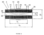
- the feedback winding (23) can be made as one turn placed at the symmetry plane, in the central part of the resonance transformer (4) ( see : Fig. 8).
- the resonance transformer (4) and the dividing high-voltage capacitor (41) can be assembled in dielectric cylinder casing (43) such as fluoroplastic and teflon so on.
- the plasma head (5) can be a kind of dielectric cap (44) with thread or fingered bushing coupling, fastener (46) at the seat (45) to the front end (47) of the casing.
- the electronic oscillations are supplied over the input (48) at the rear end (49) of the casing.
- the discharge rod-like electrode (6) has sharp, pointed emitter (50).
- the electrode (6) can be made, for instance, of bronze and it can have electrically conducting film coating, plating (51), for instance, gold.
- the plasma head is a kind of double-wall dielectric (glass) bulb (52).
- the space between the walls (55) can be filled with low pressure (for example, 1 to 20 mm Hg, that is 133.3 to 2,667 newton per square meter), normal atmospheric pressure or high pressure gas of a neutral gas, for example, helium, argon, neon, etc.
- the discharge electrode (6) comes to the internal cavity (61) of the bulb, the cavity volume is uniformly, evenly filled with electrically conducting substance (62) such as steel or copper cuts (chips), which has electric contact with the discharge electrode (63).
- the bulb is fixed to the casing (43) by means of dielectric adapters (56, 57, 58, 59).
- the plasma generator of the invention is a non-linear electronic device which generates unipolar (from one electrode) soliton mode discharge.
- the features of the unipolar discharge are dependent on resonance adjustment (amplitude, frequency, phase), on power level and high voltage level and on the type of the plasma head.
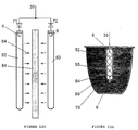
- the plasma head like the one depicted in Fig. 9B is optimum for plasma therapy in general and for plasma puncture in particular, because the plasma beam can be generated about 10 mm length and less than 1 mm diameter.
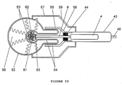
- the plasma head given in Fig. 10 forms three-dimensional (solid) discharges which are close to spherical symmetry of several types. These varying, moving cord-like discharges which diffuse three-dimensional discharges present soliton analogs of corona and spark discharges in linear circuits and devices.
- a non-linear cyclic transient of reactive energy accumulation and conversion is formed in the generalized resonance circuit (in terms of electric circuitry and field).
- the modulating transistor (3) induces free reactive power twice a period of free sine-shaped oscillation of charge (dQ 0 ) and magnetic flow (d ⁇ 0 ) at the moments of the network switching on and off. This free reactive power is emitted and absorbed by the resonance circuit.
- Non-linear features of the parametric resonance circuit are defined by three non-linear components: i.e., non-linear capacitor (17), ferrite core (22) and key-mode component (3) (for instance, transistor).
- the resonance circuit non-linearity and dispersion in terms of field processes are determined not only by the materials of the network components, but by the design of the network.
- the network integrates elements which function as transfer line, forming line and step-up transformer.
- the induction resonance process in this system differs from classical soliton excitation in electronic device.
- Combination, integration of various functions in single device brings about resonance matching of the generating resonance circuit and the load (which is the discharge). This resonance matching appears in stable field and plasma-optical solitons induced by plasma head (5).
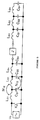
- the schematic diagram of the primary resonance circuit characterized by generalized parameters ⁇ Q 0 , ⁇ 0 , i 0 , u 0 , L 0 , C 0 ⁇ in accordance widh the equations (1) and circuitry design of Fig. 2A can be converted into a set of substitute schematic diagrams.
- This set of substitute schematic diagrams displays the development of the induction process both in time and in the proper space of the generalized resonance circuit. Possible variants of such substitute schematic diagram set are represented in Figs. 3 to 5.
- Figs. 6 and 7 depict some features of the induction process.
- L S and C S denote inductance and capacitance of layers of the resonance transformer secondary winding (31). These layers function as transfer line for the sine-shaped signal (u 0 ) and they function as forming line at the moments of the key component (transistor) driving to conduction and driving to cut-off (the key component is shown in Fig. 5 as K S ). If all the layers have the same number of turns we can roughly consider wherein,
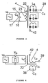
- Figs. 2B and 2C illustrate the mechanism of the spatial reactive currents generation in the circuit given in Fig. 2A.
- the current-against-voltage curve of the key component (transistor) which drives to cut-off at the moment II has the shape of triangle. This triangle bounds an area proportional to the valve reactive power. Given the direction of tracing as shown with arrows in Fig. 2B this power is negative S v ⁇ 0. It means that the Poynting's flow generation takes place in the circuit.
- the key component (3) is driving to conduction this energy is, oppositely, absorbed S v >0.
- a current source i 0 acts in the generalized network.
- Formula (3) demonstrates that this current source i 0 forms the parametric part of the induction process i 0 dL 0 /dt.
- the transient under consideration is described by Mathieu equation which is at definite initial conditions equivalent to non-linear Schrödinger equation. The latter characterizes soliton excitations in the system.
- Fig. 6A shows the current versus voltage characteristic of the double forming line ( see : Fig. 5) which is the generating part of the parametric resonance circuit ( see : Fig. 2).
- Fig. 7 presents one of the variants of soliton waves in the parametric circuit.
- the discharge process starts and completes at the same single electrode.
- the soliton has a core and a tail ("fur-coat"):
- the core is observed as a bright luminescence (thin layer) around the main electrode and it contains more than 90% of all the energy generated by the parametric circuit, where all generated energy is defined by the area within the current-against-voltage curve in Fig. 6A and the soliton tail contains small part of energy and it forms filaments, cords similar to plasma or diffuse luminescence.
- the discharge from the single electrode can be in the form of corona, spark or arc discharge.
- the discharge current J appears as a result of tunneling of the reactive current (or Poynting's flow) through dielectric layer.
- the plasma generator presents a reactive analog of Josephson effect device.
- u 0 corresponds to the potential difference at the Josephson contact.
- the stable form of the soliton reactive current depends on the generalized resonance circuit non-linearity and dispersion which are defined by non-linear materials and geometrical proportions of the transformer ( see : Fig. 8).
- the material was bronze and plating was gold.
- the accommodating (dividing, decoupling) capacitor (41) before the rod-like electrode changes the soliton core localization and the conventional potential difference at the Josephson contact. Thus the requirements of plasmapuncture are met (to reduce the output potential ⁇ 0 ).
- the value of 2-50 pF is practical.
- the power consumption of medical, biological applications of the generator does not exceed 2-40 W.
- the output potential ⁇ 0 0.5-10 kV.
- the carrier resonance frequency f 0 20-200 kHz.
- the rod-like electrode with pointed emitter provides for visible plasma beam formation about 10 mm length, tens or hundreds of micrometer diameter. This is fairly useful, functional for plasma-puncture.
- Any functional part of the invented plasma generator can be combined, either completely or in a certain portion, with another functional part (or other functional parts) in a single unit, component, device (in a number of units, components, devices).
- the discharge electrode made of electrically conducting material can have another, especial form, different from the pointed rod.
- the plasma generator can have the discharge electrode coming to the inner space of hermetically sealed dielectric bulb, envelope, filled with gas and/or liquid and/or solid structure, the pressure and the composition of the gas and other parameters of the contents of the bulb, envelope, being chosen in accordance with the specified requirements on the plasma features.
- the discharge electrode dielectric or semiconductor extensions can be used as well.
- the discharge electrode gas and/or aerosol and/or liquid dynamic extensions can be used; they present gas and/or aerosol and/or liquid stream (jet) produced by special device.
- a compressor, a fan, or a bottled gas, gas cylinder can be used in such device.
- the discharge electrode extension can also present a combination of electric conductor and/or semiconductor and/or dielectric and/or mixed composition parts, components, elements of arbitrary forms and in arbitrary geometrical and electrical configurations, and among those parts, components, elements there can be common, ordinary and/or special, original devices, components, for instance, there can be sealed, hermetic dielectric bulbs, envelopes, either exhausted or filled with some substance or some composition of substances.
- Plasmon beam (64) similar to the plasmon beam shown in Fig. 9 can also be formed by composite conductor & dielectric (6 & 65) tube electrode assembly presented in Fig. 11A.
- Gas (66), neutral for instance, is coming into dielectric tube (65) and then the gas is being magnetically activated during passage inside parametric resonance transformer (4) to form gas-magnetic focusing lens (67) around the beam (64).
- the metal tube section (6) can be built in dielectric sleeve (68) that functions as an isolator mounting support for high voltage lead (39) of the resonance transformer (4).
- the discharge electrode extension can be formed not only by gas flow (stream) but also by liquid (fluid) and/or aerosol flow generated by special device.
- Fig. 11B displays plasmon head with tube electrode assembly. It can contain a number of dielectric (65) and conductor (metal) (6) elements in line.
- the processing zone (technological space) (69) filled with water system or another liquid, fluid (70) is activated by both beam (64) and flow (67).
- Plasmon unit can also contain two high frequency high voltage semiconductor diodes, (71) and (72), connected to the lead (39) of the resonance transformer (4) as shown in Fig. 11C.
- the processing (technological) chamber (69) is filled with substance (70), it can be gas and/or liquid and/or aerosol and/or powder, dust.
- Conductor electrodes (73) and (74) are placed symmetrically against the resonance transformer (4) axis.
- the ring chamber (69) can be made of molybdenum glass or quartz, it has a spherical expansion (75) in which a filter (76) is built.
- Fig. 11D shows technological chamber with metal electrodes (73) and (74) made as plates of metal which actively absorbs hydrogen, it can be zirconium, titan, niobium, tantalum.
- the discharge currents (64) that pass between the electrodes (73) and (74) can have the form of diffuse discharge which fills all the volume of the medium (70) being activated.
- the walls of the chamber work as catalyst for various reactions in the area of contact with the medium.
- the load currents in the mode of parametric resonance are formed as soliton waves.
- These soliton waves consist of quasi-particles of various types (for instance, of magnons and phonons). Varying the material and the shape of the electrode and electrode extension (metals, alloys, semiconductors, dielectric) one can vary intensity and form of the quasi-particles currents in plasmon unit. These currents are originated as non-force collective excitation of crystal structures at the surface and inside the body of electrode assembly. If excitation of electrons in the crystal body of electrodes (6) dominates, the load currents are produced in the form of plasmons (waves and quasi-particles in the pulse space of metal electrodes).
- Dielectric electrode extensions (69) which work as the processing chambers induce also specific quasi-particle types (at the surface and inside the body), polarons. The polarons are caused by the chosen dielectric polarization.
- Figs. 12A, 12B, 12C and 12D show various plasmon-optic units which serve both as converters and as loads for soliton waves. These soliton waves consist of direct and reverse currents of quasi-particles.
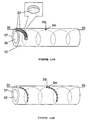
- the optic head (unit) in the form of flat spiral tube (77), Fig. 12A, is excited from high voltage lead (39) and conductor cylinder electrode (6).
- the envelope (52) is made of glass.
- the end (78) of the tube is hermetically sealed.
- the internal space (55) is filled with low-pressure gas, it can be neutral, for instance.
- the unit is constructed as a single pole (monopolar) tube with one lead electrode (6) which induces a package of soliton waves-currents into the working volume.
- These soliton waves-currents consist of plasmons and optical phonons which form quantum flow (64) at the surface (52).
- the quantum flow (64) consists of mutually converted photons and optical phonons.
- Plasmon-optical unit can also be assembled from common, general U-shaped gas discharge tubes with luminescent lining (79)( see : Fig. 12B).
- the tubes are connected in series, "snake-like".
- the connections are made by conductor electrodes (80), and an electrode (81) is connected to the end of the assembly.
- the alternating parametric high voltage from the lead (39) is transferred to all the intermediate electrodes (80) and the final electrode (81).
- Optical unit displayed in Fig. 12C generates effectively currents of quasi-particles (excitons and polarons).
- the dielectric (tube) sub-units (82) and (83) can be the flat spiral tubes (Fig. 12A) or the "snake-like" U-tube assemblies (Fig. 12B) or "flat array” assemblies from general rod-shaped gas discharge luminescent tubes.
- Monopolar connection to the parametric resonance lead (39) is implemented by metal electrode (6) and semiconductor diodes (71), (72) (high frequency high voltage diodes).
- processing is placed in the middle of the space between the two polar optical sub-units (82) and (83).
- a cylindrical vacuum tube (bulb) with glass envelope (52) and two metal rod electrodes (6) at the ends can be used for activation of gas and/or liquid (fluid)( see : Fig. 12D).
- a wave current process is developing from the upper electrode (6) in the form of two solid (3-D, spatial) sinusoids. These two sinusoids are growing and then reach the lower electrode (6). After it the two sinusoids begin to rotate about the vertical symmetry axis.
- Emission (64) covers the technological chamber (69) and interacts with the medium (70) to be processed. This emission consists of several types of quasi-particles (plasmons, phonons, magnons).
- the plasmotronic load unit of the generator can be implemented as a system of flat conductor plates (73) and (74) shown in Fig. 13A.
- the object of activation (84) such as dielectric film, wafer, plate, is placed between the conductor plates (73), (74).
- Semiconductor diodes (71) and (72) are connected to the flat electrode (73).
- Capacitor (85) closes the diodes.
- the flow of quasi-particles (64) which transfers the charges, currents in the gape (space) between the plates (73) and (74) can be considered as Josephson current which tunnels through dielectric (the object) in accordance with equations (9)-(11).
- the excessive, extra charge transferred by the quasi-particles (polarons, excitons, etc.) is accumulated and charges the capacitor (85).
- the flow of reactive power can be controlled and the technological process can be adjusted, optimized.
- Fig. 13B shows technological plasmotronic unit for processing of free-flowing bulk materials in order to control their properties, features.
- This unit is also used to control the properties of polycrystal substance in the state of phase transition. For instance, the unit is used to control the process of silicon monocrystal (single crystal) growing by Chokhralsky method.
- the technological chamber (graphite or quartz crucible) (69) with polycrystal substance (silicon) (70) is placed in the center of semi-cylinder electrode structure (73), (74).
- the electrodes (73) and (74) are made of refractory, high-melting-point metal. They also function as heat shields.
- the flow (64) of reactive quasi-particles passes the technological zone between the electrodes and brings about resonance parametric excitation of the processed substance.
- parameters of the substance as heat capacity (specific heat), magnetic susceptibility or dielectric constant (permittivity) can be varied. It is possible to predict, to design and realize various types of phase transition, to derive, obtain various properties, parameters of substance if the dispersion characteristics of the processed substance (load) and the type of non-linearity of the parametric resonance generator are known.
- Metal electrode system can be quadrupolar, as shown in Fig. 13C. Additional pair of electrodes (86), (87) is installed across the first pair (73), (74). The additional electrodes are connected through semiconductor diodes (88) and (89).
- Fig. 14 shows pipe-shaped structure (93) with tablet (button) diodes (92).
- the diodes can be encapsulated, baked, caked, sintered in epoxy compound along helical (helix) line in cylinder layer (97).
- the cylinder hollow (98) serves as the passage of the processed gases and/or aerosols and/or liquids (fluids) and/or free-flowing bulk substances.
Landscapes
- Physics & Mathematics (AREA)
- Engineering & Computer Science (AREA)
- Plasma & Fusion (AREA)
- Chemical & Material Sciences (AREA)
- Analytical Chemistry (AREA)
- Electromagnetism (AREA)
- Spectroscopy & Molecular Physics (AREA)
- Plasma Technology (AREA)
Abstract
The present invention relates to a plasma generator to
apply cold plasma in the fields of medicine, biology,
ecological recovery, activation, purification, special
processing of gases, liquids and solid substances as well
as other areas of technology and science. A plasma
generator of the invention comprises: a power source (7); an
electronic oscillator (1) constructed on an amplifying
(control) element (3) which is connected to a low voltage
input section (14); a resonance transformer (4) having a low
voltage input section (14) and a high voltage output section (31);
and, one pin of the high voltage output section (31) of the
resonance transformer which is connected to a discharge
electrode (6). The present invention provides a universal
plasma generator with decreased mass and dimensions which
provides unipolar plasma for plasma therapy and activation
of substantial media by virtue of the field.
Description
The present invention relates to a plasma generator,
more specifically, to a plasma generator to apply cold
plasma in the fields of medicine, biology, ecological
recovery, activation, purification, special processing of
gases, liquids and solid substances as well as other areas
of technology and science.
Plasmotrons which can generate plasma under normal
atmospheric pressure conditions with temperature up to
thousands degrees Celsius are well known in the art. The
thermal heating of plasma is actived by classical
electromagnetic induction, via induction heating of
electrically conducting media in alternating
electromagnetic field of the inductor. The device
consists of high voltage AC generator, quartz pipe-shaped
case and liquid-cooled inductor, an inductance coil having
large numbers of turns. In order to generate the
induction discharges in a volume of approximately 1 liter
(0.001 m3), a multi-turn inductor of 0.1 m diameter is
essentially required, the inductor reactance being raised
greatly at 1 MHz and higher frequencies. Naturally, it is
very difficult to match the high voltage generator with
the inductor reactance, and the effective output power is
decreased. Accordingly, the prior art plasmotron has
revealed some drawbacks of large dimensions, poor
efficiency and very high plasma temperature, which, in
turn, restricted its operational features considerably,
especially in medicine, biology and ecological treatment.
The other types of plasma generator have been used in
electric discharge therapy device which comprise
electronic oscillator, modulation unit, output resonance
transformer and rod-like discharge electrode. A plasma
beam is induced between the end of the electrode and the
biological object. The electronic oscillator produces
oscillations in 200 kHz through 300 kHz frequency range.
The modulator which can be constructed in transistors
periodically switches on and off the signal of the
oscillator at about 3 kHz to 5 kHz rate. Thus, the
modulator provides impact excitation of resonance
transformer circuit, which brings about measured output
emission in a form of corona discharge between the
electrode and the object. The device produces favorable
therapeutic effect to treat a number of diseases,
disorders, pathologies, mainly due to the induced heat in
the specified areas of body.
The device, however, has also revealed shortcomings
that the discharge transformation from corona to spark
form may be appeared and the conduction currents
origination directly in the tissue. The classical corona
and spark discharge inevitably results in ionization,
electric break-through and thermal heating of the air gap
between the inducing electrode and the body which is used
as the second electrode. Moreover, direct resonance
action of the device by virtue of field is shunted as a
result of ionization of substantial medium and chaotic
heat motion of particles in the discharge area.
The said problems of the prior art plasma generator,
in principle, have limited all the direct use of
electromagnetic field in medicine, biology and directed
activation of substantial media such as gases, liquids and
solid bodies. Under the circumstances, there are strong
reasons for exploring and developing alternative type of a
novel plasma generator to solve said problems in the art.
A primary object of the invention is, therefore, to
provide a universal plasma generator with decreased mass
and dimensions which provides unipolar plasma for plasma
therapy and activation of substantial media by virtue of
the field.
The above objects of the present invention will become
apparent from the following descriptions given in
conjunction with the accompanying drawings, in which:
- Fig. 1
- is a structural circuit diagram of the plasma generator of the present invention;
- Fig. 2A
- is an unit-block diagram of the primary parametric resonance circuit;
- Fig. 2B
- is a curve of current versus voltage at the key element (key-mode transistor);
- Fig. 2C
- is a plot of current and voltage in the resonance circuit;
- Fig. 3
- is a substitution schematic diagram to the resonance transformer with regard to sine-shaped signal flow;
- Fig. 4
- is a substitution schematic diagram to the resonance transformer with regard to binary driving signal flow;
- Fig. 5
- is a substitution schematic diagram to the secondary multi-layer winding of the transformer considered as a double forming line;
- Fig. 6A
- is a curve of current versus voltage at the double forming line in the mode of reactive power generation, Qc < 0;
- Fig. 6B
- is a plot of instantaneous reactive resistance in the resonance circuit;
- Fig. 7
- shows soliton generation process in the secondary (high voltage) section of the resonance transformer, the secondary section functions in a forming line mode;
- Fig. 8
- shows an example of the parametric resonance transformer which combines functions of transfer and forming lines;
- Fig. 9A
- is a brief cross-sectional view of the generator high voltage unit with plasma head and unipolar rod-like electrode;
- Fig. 9B
- is a brief cross-sectional view of the unipolar rod-like electrode;
- Fig. 10
- is a brief cross-sectional view of the generator high voltage unit with plasma head;
- Fig. 11A
- shows plasmon head (working probe) with two-section metal-dielectric tube electrode assembly; gas and/or aerosol flow is passed through this electrode assembly;
- Fig. 11B
- shows plasmotron head with multi-section tube electrode assembly for activation of liquids, fluids, for instance, water solutions (systems);
- Fig. 11C
- shows plasmotron head (unit) with dielectric ring electrode assembly and semiconductor diode polarizers for activation of liquids, fluids, for instance, water solutions (systems);
- Fig. 11D
- shows plasmotron unit with polarizing semiconductor elements and conductor plate electrode assembly;
- Fig. 12A
- shows plasmon-optic head (unit) in the form of flat spiral tube, bulb with conductor electrode at the end;
- Fig. 12B
- shows plasmon-optic head (unit) with U-shaped gas-discharge tubes connected in series;
- Fig. 12C
- shows plasmon-emission unit with semiconductor polarizers and a system of gas-discharge tubes placed so that to form special spatial configuration;
- Fig. 12D
- shows plasmotronic unit with tube having two electrodes at the ends which forms rotating soliton field;
- Fig. 13A
- shows emission unit with flat electrodes for activation of plates, wafers, films;
- Fig. 13B
- shows plasmotronic unit with flat or semi-cylinder electrodes for volume (3-D, solid) polarization and activation of powders, dusts as well as gases, fluids, liquids;
- Fig. 13C
- shows plasmotronic quadrupolar electrode system for activation of the technological zones, areas, volumes;
- Fig. 14A
- shows construction of pipe-shaped electrode extension with tablet (button) semiconductor diodes placed along a helical line;
- Fig. 14B
- shows circuitry diagram of pipe-shaped electrode extension with tablet (button) semiconductor diodes placed along a helical line.
A plasma generator of the invention comprises:
A preferred embodiment of the present invention is
explained in detail with references on the accompanying
drawings, which should not be taken to limit the scope of
the invention. In particular, the description of certain
parts or components of the preferred embodiment and their
connections and interactions given below should not be
taken to limit the scope of the present invention.
Referring to Fig. 1, a structural circuit diagram of
the plasma generator of the present invention is shown
schematically.
The plasma generator employs a conventional DC power
source (7), which consists of AC voltage reducing
transformer (8), bridge rectifier (9) and capacitor filter
(10). The structure of the primary resonance circuit (13)
constituting the electronic oscillator (1) involves non-linear
capacitor (17) as well as the input low voltage
section (14) of the resonance transformer (4). The
primary resonance circuit (13) also includes an amplifying
(control) element (3), e.g., a transistor.
The plasma generator is optionally equipped with a
drive unit (2) which is connected to the amplifying
(control) element (3) and provides cyclic switching on and
off of the amplifying (control) element (3) or another
special drive mode. The drive unit (2) can be made with
an electronic integrated circuit or diode-resistor
assembly.
The parametric resonance transformer (4) can be
realized as an induction multi-turn coil transformer. In
many cases, it makes sense to furnish the resonance
transformer (4) with ferrite core (22). Feedback section
(23) of the resonance transformer (4) is connected to
control input (27) of the amplifying (control) element
(3). A junction capacitor (26), correction resistors (28,
29) and diode (30) can be used for optimal operational
conditions. The high voltage output section (31) of the
resonance transformer (4) that is the secondary multilayer
winding, is placed directly at the ferrite core
(22). This high voltage output section (31) consists of
inductive layers (32, 33, 34 and so on), whose number can
be 10 to 20. The layer capacitance (35, 36, 37) which
forms a cell (38) of transfer line in conjunction with the
inductive layers. The line is combined with the electric
circuit of the parametric transformer secondary winding.
The lead (39) of the secondary winding internal layer is
connected to rod-like electrode (6) in plasma head (5) via
dividing (coupling) capacitor (41). The lead (42) of the
secondary winding external layer can be either isolated or
connected to the lead (16) of the primary winding (14).
The primary winding (14) can be winded in one layer atop
the secondary winding. The feedback winding (23) can be
made as one turn placed at the symmetry plane, in the
central part of the resonance transformer (4) (see: Fig.
8).
As can be seen in Figs. 9A and 9B, the resonance
transformer (4) and the dividing high-voltage capacitor
(41) can be assembled in dielectric cylinder casing (43)
such as fluoroplastic and teflon so on. The plasma head
(5) can be a kind of dielectric cap (44) with thread or
fingered bushing coupling, fastener (46) at the seat (45)
to the front end (47) of the casing. The electronic
oscillations are supplied over the input (48) at the rear
end (49) of the casing. The discharge rod-like electrode
(6) has sharp, pointed emitter (50). The electrode (6)
can be made, for instance, of bronze and it can have
electrically conducting film coating, plating (51), for
instance, gold.
As can be seen in Fig. 10, the plasma head is a kind
of double-wall dielectric (glass) bulb (52). The space
between the walls (55) can be filled with low pressure
(for example, 1 to 20 mm Hg, that is 133.3 to 2,667 newton
per square meter), normal atmospheric pressure or high
pressure gas of a neutral gas, for example, helium, argon,
neon, etc. The discharge electrode (6) comes to the
internal cavity (61) of the bulb, the cavity volume is
uniformly, evenly filled with electrically conducting
substance (62) such as steel or copper cuts (chips), which
has electric contact with the discharge electrode (63).
The bulb is fixed to the casing (43) by means of
dielectric adapters (56, 57, 58, 59).
The plasma generator of the invention is a non-linear
electronic device which generates unipolar (from one
electrode) soliton mode discharge. The features of the
unipolar discharge are dependent on resonance adjustment
(amplitude, frequency, phase), on power level and high
voltage level and on the type of the plasma head. The
plasma head like the one depicted in Fig. 9B is optimum
for plasma therapy in general and for plasma puncture in
particular, because the plasma beam can be generated about
10 mm length and less than 1 mm diameter. The plasma head
given in Fig. 10 forms three-dimensional (solid)
discharges which are close to spherical symmetry of
several types. These varying, moving cord-like discharges
which diffuse three-dimensional discharges present soliton
analogs of corona and spark discharges in linear circuits
and devices.
The operation mode of the preferred embodiment of the
plasma generator of the invention is described in detail
with references on the accompanying drawings.
Parametric resonance is excited in the primary
resonance circuit (13) (see: Fig. 1), which corresponds to
the generalized electromagnetic induction law, charge and
magnetic flow total (perfect, exact, ordinary)
differentials, dQ and dψ, connected to the primary circuit
being represented by the following equations:
 wherein,
- C0
- is equivalent capacitance;
- L0
- is equivalent inductance;
- u0
- is voltage; and,
- i0
- is current in the generalized resonance circuit.
A non-linear cyclic transient of reactive energy
accumulation and conversion is formed in the generalized
resonance circuit (in terms of electric circuitry and
field). The modulating transistor (3) induces free
reactive power twice a period of free sine-shaped
oscillation of charge (dQ0) and magnetic flow (dψ0) at the
moments of the network switching on and off. This free
reactive power is emitted and absorbed by the resonance
circuit.
Non-linear features of the parametric resonance
circuit are defined by three non-linear components: i.e.,
non-linear capacitor (17), ferrite core (22) and key-mode
component (3) (for instance, transistor).
The resonance circuit non-linearity and dispersion in
terms of field processes are determined not only by the
materials of the network components, but by the design of
the network. The network integrates elements which
function as transfer line, forming line and step-up
transformer. The induction resonance process in this
system differs from classical soliton excitation in
electronic device. Combination, integration of various
functions in single device (when the wave resonance is
described by partial differential equations) brings about
resonance matching of the generating resonance circuit and
the load (which is the discharge). This resonance
matching appears in stable field and plasma-optical
solitons induced by plasma head (5).
Therefore, the schematic diagram of the primary
resonance circuit characterized by generalized parameters
{Q0, ψ0, i0, u0, L0, C0} in accordance widh the equations
(1) and circuitry design of Fig. 2A can be converted into
a set of substitute schematic diagrams. This set of
substitute schematic diagrams displays the development of
the induction process both in time and in the proper space
of the generalized resonance circuit. Possible variants
of such substitute schematic diagram set are represented
in Figs. 3 to 5.
Figs. 6 and 7 depict some features of the induction
process.
The following designations are used: LS and CS denote
inductance and capacitance of layers of the resonance
transformer secondary winding (31). These layers function
as transfer line for the sine-shaped signal (u0) and they
function as forming line at the moments of the key
component (transistor) driving to conduction and driving
to cut-off (the key component is shown in Fig. 5 as KS).
If all the layers have the same number of turns we can
roughly consider
wherein,
The induction process in the resonance circuit under
consideration is described not only with circuitry
equations, but also with equations for Poynting's flow
which closes on itself inside the proper space of the
generalized network.
It can be shown that the second terms in equations (1)
generate scalar electric field E0 and scalar magnetic
field H0. Therefore, the complete substitute circuitry of
the layers of the transformer winding which functions as a
line (see: Fig. 5) represents double line. In Fig. 5, the
left and right parts of the double line represent the
induction process versus time (1/dt) and the induction
process versus space coordinates (1/dx), respectively.
There exists direct and reverse (feedback) magnetic
and electric couplings between the double line elements,
i.e., M12 and N12. The load for the double forming line is
a current source J which reflects the process of plasma
generation. A similarity of this phenomenon to Josephson
effect will be demonstrated later.
Another characteristic feature of the set of the
substitute schematic diagrams of the soliton induction
process consists in reactive form of the spatial currents
in the line. Therefore, in order to reflect "orthogonal
turn" of the Poynting's flow in the parametric circuit the
magnetic network is shown as orthogonal one in Fig 4.
This process for magnetic flow has the following
expression:
dψ0 dt = L0 di0 dt + i0 dL0 dt
wherein,
ψ0 = L0 i0
The conditions of the parametric resonance excitation
are:
ω0 = ω1 ω0 2 = 1L0 C0 m > 2Q
wherein,
- ω0
- is the proper resonance frequency of the circuit, the frequency of discharge in the plasma head (5) being equal to the ω0;
- ω1
- is the frequency of u0 source;
- m
- is modulation coefficient of generalized inductance; and,
- Q
- is the circuit merit factor.
Figs. 2B and 2C illustrate the mechanism of the
spatial reactive currents generation in the circuit given
in Fig. 2A. The current-against-voltage curve of the key
component (transistor) which drives to cut-off at the
moment II has the shape of triangle. This triangle bounds
an area proportional to the valve reactive power. Given
the direction of tracing as shown with arrows in Fig. 2B
this power is negative Sv<0. It means that the Poynting's
flow generation takes place in the circuit. When the key
component (3) is driving to conduction this energy is,
oppositely, absorbed Sv>0. Thus a current source i0 acts
in the generalized network. Formula (3) demonstrates that
this current source i0 forms the parametric part of the
induction process i0 dL0/dt. The transient under
consideration is described by Mathieu equation which is at
definite initial conditions equivalent to non-linear
Schrödinger equation. The latter characterizes soliton
excitations in the system.
Fig. 6A shows the current versus voltage
characteristic of the double forming line (see: Fig. 5)
which is the generating part of the parametric resonance
circuit (see: Fig. 2). The area bounded by the curve is
proportional to the generated power of the plasmoid. The
generation occurs only when the ratio of the u0 and i0
instantaneous values varies:
z0 (t) = u0 (t)i0 (t) = var
In those modes when z0(t) is constant and S0=0, the
soliton field excitations do not occur and the device
functions in linear mode.
Fig. 7 presents one of the variants of soliton waves
in the parametric circuit.
For the said two types of the plasma head described
above which have rod-like unipolar electrode depicted in
Fig. 9B and quasi-spherical electrode inside double wall
bulb depicted in Fig. 10, the discharge process starts and
completes at the same single electrode. In both cases the
soliton has a core and a tail ("fur-coat"): The core is
observed as a bright luminescence (thin layer) around the
main electrode and it contains more than 90% of all the
energy generated by the parametric circuit, where all
generated energy is defined by the area within the
current-against-voltage curve in Fig. 6A and the soliton
tail contains small part of energy and it forms filaments,
cords similar to plasma or diffuse luminescence. They
have continuous wide frequency spectrum and they are
healthful, they provide positive biotherapeutic effect.
Depending on the environment characteristics (atmospheric
pressure or vacuum of 1 to 20 mm Hg, that is 133.3 to
2,667 newton per square meter, presence of argon, helium,
neon) as well as on the process intensity (u0 and i0
largeness) and on the value (range) of the main carrier
frequency (ω0) the discharge from the single electrode can
be in the form of corona, spark or arc discharge.
However, this is actually an induction process in the
proper space of the excited parametric circuit. The
discharge current J appears as a result of tunneling of
the reactive current (or Poynting's flow) through
dielectric layer. In other words, the plasma generator
presents a reactive analog of Josephson effect device.
If the reactive alternating potential value at the
unipolar electrode is ϕ0 and the process in the non-linear
circuit of Fig. 2 is described by Sin-Gordon equation, the
following expression is valid:
∂2 ϕ0 ∂ x2 - ∂2 ϕ0 ∂ t2 = sin ϕ0
wherein,
∂ ϕ0 ∂ t = 2πψ0 u0
u0 corresponds to the potential difference at the
Josephson contact. In our case u0 is defined by
parametric resonance and the circuit transformation
factor. Therefore, from the formulae (9) and (10) and
from the substitution schematic diagram Fig. 5 it follows
that the plasma generator output current J is determined
by:
J = i0 sin ϕ0
The stable form of the soliton reactive current
depends on the generalized resonance circuit non-linearity
and dispersion which are defined by non-linear materials
and geometrical proportions of the transformer (see: Fig.
8). Optimum proportions for the frequency range f0 =20-100
kHz are the following:
 wherein,
- D1 and D2
- are the inner and the outer diameters of the secondary cylindrical winding; and,
- h1
- is the length of the secondary cylindrical winding.
Certain specific variants of the rod-like electrode
were implemented with the following dimensions (see: Fig.
9B): the length l0 = 10-15 mm, the diameter d0 = approx. 1
mm, the emitter length Δ = 2-4 mm. The material was
bronze and plating was gold.
The accommodating (dividing, decoupling) capacitor
(41) before the rod-like electrode changes the soliton
core localization and the conventional potential
difference at the Josephson contact. Thus the
requirements of plasmapuncture are met (to reduce the
output potential ϕ0). The value of 2-50 pF is practical.
The power consumption of medical, biological
applications of the generator does not exceed 2-40 W. The
output potential ϕ0 = 0.5-10 kV. The carrier resonance
frequency f0 = 20-200 kHz. The rod-like electrode with
pointed emitter provides for visible plasma beam formation
about 10 mm length, tens or hundreds of micrometer
diameter. This is fairly useful, functional for plasma-puncture.
Any functional part of the invented plasma generator
can be combined, either completely or in a certain
portion, with another functional part (or other functional
parts) in a single unit, component, device (in a number of
units, components, devices).
Various types and modifications of the discharge
electrodes (working probes, working heads) and auxiliary
extensions to them can be used.
The discharge electrode made of electrically
conducting material (substance) can have another, especial
form, different from the pointed rod.
The plasma generator can have the discharge electrode
coming to the inner space of hermetically sealed
dielectric bulb, envelope, filled with gas and/or liquid
and/or solid structure, the pressure and the composition
of the gas and other parameters of the contents of the
bulb, envelope, being chosen in accordance with the
specified requirements on the plasma features.
The discharge electrode dielectric or semiconductor
extensions can be used as well. The discharge electrode
gas and/or aerosol and/or liquid dynamic extensions can be
used; they present gas and/or aerosol and/or liquid stream
(jet) produced by special device. A compressor, a fan, or
a bottled gas, gas cylinder can be used in such device.
The discharge electrode extension can also present a
combination of electric conductor and/or semiconductor
and/or dielectric and/or mixed composition parts,
components, elements of arbitrary forms and in arbitrary
geometrical and electrical configurations, and among those
parts, components, elements there can be common, ordinary
and/or special, original devices, components, for
instance, there can be sealed, hermetic dielectric bulbs,
envelopes, either exhausted or filled with some substance
or some composition of substances.
Plasmon beam (64) similar to the plasmon beam shown in
Fig. 9 can also be formed by composite conductor &
dielectric (6 & 65) tube electrode assembly presented in
Fig. 11A. Gas (66), neutral for instance, is coming into
dielectric tube (65) and then the gas is being
magnetically activated during passage inside parametric
resonance transformer (4) to form gas-magnetic focusing
lens (67) around the beam (64). The metal tube section
(6) can be built in dielectric sleeve (68) that functions
as an isolator mounting support for high voltage lead (39)
of the resonance transformer (4).
The discharge electrode extension can be formed not
only by gas flow (stream) but also by liquid (fluid)
and/or aerosol flow generated by special device. Fig. 11B
displays plasmon head with tube electrode assembly. It
can contain a number of dielectric (65) and conductor
(metal) (6) elements in line. The processing zone
(technological space) (69) filled with water system or
another liquid, fluid (70) is activated by both beam (64)
and flow (67).
Plasmon unit can also contain two high frequency high
voltage semiconductor diodes, (71) and (72), connected to
the lead (39) of the resonance transformer (4) as shown in
Fig. 11C. The processing (technological) chamber (69) is
filled with substance (70), it can be gas and/or liquid
and/or aerosol and/or powder, dust. Conductor electrodes
(73) and (74) are placed symmetrically against the
resonance transformer (4) axis. The ring chamber (69) can
be made of molybdenum glass or quartz, it has a spherical
expansion (75) in which a filter (76) is built.
Fig. 11D shows technological chamber with metal
electrodes (73) and (74) made as plates of metal which
actively absorbs hydrogen, it can be zirconium, titan,
niobium, tantalum. The discharge currents (64) that pass
between the electrodes (73) and (74) can have the form of
diffuse discharge which fills all the volume of the medium
(70) being activated. In this case the walls of the
chamber work as catalyst for various reactions in the area
of contact with the medium.
In the plasma generators of Figs. 11C and 11D the load
currents in the mode of parametric resonance are formed as
soliton waves. These soliton waves consist of quasi-particles
of various types (for instance, of magnons and
phonons). Varying the material and the shape of the
electrode and electrode extension (metals, alloys,
semiconductors, dielectric) one can vary intensity and
form of the quasi-particles currents in plasmon unit.
These currents are originated as non-force collective
excitation of crystal structures at the surface and inside
the body of electrode assembly. If excitation of
electrons in the crystal body of electrodes (6) dominates,
the load currents are produced in the form of plasmons
(waves and quasi-particles in the pulse space of metal
electrodes). Semiconductor diodes (71) and (72) induce
parametric excitation of excitons (electron - electron
vacancy pair) in the semiconductor crystal structure.
Dielectric electrode extensions (69) which work as the
processing chambers induce also specific quasi-particle
types (at the surface and inside the body), polarons. The
polarons are caused by the chosen dielectric polarization.
Figs. 12A, 12B, 12C and 12D show various plasmon-optic
units which serve both as converters and as loads for
soliton waves. These soliton waves consist of direct and
reverse currents of quasi-particles.
The optic head (unit) in the form of flat spiral tube
(77), Fig. 12A, is excited from high voltage lead (39) and
conductor cylinder electrode (6). The envelope (52) is
made of glass. The end (78) of the tube is hermetically
sealed. The internal space (55) is filled with low-pressure
gas, it can be neutral, for instance. So, the
unit is constructed as a single pole (monopolar) tube with
one lead electrode (6) which induces a package of soliton
waves-currents into the working volume. These soliton
waves-currents consist of plasmons and optical phonons
which form quantum flow (64) at the surface (52). The
quantum flow (64) consists of mutually converted photons
and optical phonons.
Plasmon-optical unit can also be assembled from
common, general U-shaped gas discharge tubes with
luminescent lining (79)(see: Fig. 12B). The tubes are
connected in series, "snake-like". The connections are
made by conductor electrodes (80), and an electrode (81)
is connected to the end of the assembly. During emission
of optical phonons and tunneling of currents according to
formulas (9)-(11) the alternating parametric high voltage
from the lead (39) is transferred to all the intermediate
electrodes (80) and the final electrode (81).
Optical unit displayed in Fig. 12C generates
effectively currents of quasi-particles (excitons and
polarons). The dielectric (tube) sub-units (82) and (83)
can be the flat spiral tubes (Fig. 12A) or the "snake-like"
U-tube assemblies (Fig. 12B) or "flat array"
assemblies from general rod-shaped gas discharge
luminescent tubes. Monopolar connection to the parametric
resonance lead (39) is implemented by metal electrode (6)
and semiconductor diodes (71), (72) (high frequency high
voltage diodes). In this case the object (84) of
activation, processing (resonance control of parameters)
is placed in the middle of the space between the two polar
optical sub-units (82) and (83).
A cylindrical vacuum tube (bulb) with glass envelope
(52) and two metal rod electrodes (6) at the ends can be
used for activation of gas and/or liquid (fluid)(see: Fig.
12D). During the course of rising of voltage at the lead
(39) a wave current process is developing from the upper
electrode (6) in the form of two solid (3-D, spatial)
sinusoids. These two sinusoids are growing and then reach
the lower electrode (6). After it the two sinusoids begin
to rotate about the vertical symmetry axis. Emission (64)
covers the technological chamber (69) and interacts with
the medium (70) to be processed. This emission consists
of several types of quasi-particles (plasmons, phonons,
magnons).
The plasmotronic load unit of the generator can be
implemented as a system of flat conductor plates (73) and
(74) shown in Fig. 13A. The object of activation (84),
such as dielectric film, wafer, plate, is placed between
the conductor plates (73), (74). Semiconductor diodes
(71) and (72) are connected to the flat electrode (73).
Capacitor (85) closes the diodes. The flow of quasi-particles
(64) which transfers the charges, currents in
the gape (space) between the plates (73) and (74) can be
considered as Josephson current which tunnels through
dielectric (the object) in accordance with equations (9)-(11).
The excessive, extra charge transferred by the
quasi-particles (polarons, excitons, etc.) is accumulated
and charges the capacitor (85). Thus the flow of reactive
power can be controlled and the technological process can
be adjusted, optimized.
Fig. 13B shows technological plasmotronic unit for
processing of free-flowing bulk materials in order to
control their properties, features. This unit is also
used to control the properties of polycrystal substance in
the state of phase transition. For instance, the unit is
used to control the process of silicon monocrystal (single
crystal) growing by Chokhralsky method. The technological
chamber (graphite or quartz crucible) (69) with
polycrystal substance (silicon) (70) is placed in the
center of semi-cylinder electrode structure (73), (74).
The electrodes (73) and (74) are made of refractory, high-melting-point
metal. They also function as heat shields.
The flow (64) of reactive quasi-particles passes the
technological zone between the electrodes and brings about
resonance parametric excitation of the processed
substance. Such parameters of the substance as heat
capacity (specific heat), magnetic susceptibility or
dielectric constant (permittivity) can be varied. It is
possible to predict, to design and realize various types
of phase transition, to derive, obtain various properties,
parameters of substance if the dispersion characteristics
of the processed substance (load) and the type of non-linearity
of the parametric resonance generator are known.
Metal electrode system can be quadrupolar, as shown in
Fig. 13C. Additional pair of electrodes (86), (87) is
installed across the first pair (73), (74). The
additional electrodes are connected through semiconductor
diodes (88) and (89).
Fig. 14 shows pipe-shaped structure (93) with tablet
(button) diodes (92). The diodes can be encapsulated,
baked, caked, sintered in epoxy compound along helical
(helix) line in cylinder layer (97). The cylinder hollow
(98) serves as the passage of the processed gases and/or
aerosols and/or liquids (fluids) and/or free-flowing bulk
substances.
Claims (13)
- A plasma generator, comprising:means for transforming a resonance having a low voltage input section and a high voltage output section, wherein the high voltage output section includes a pin;first means for generating an oscillation signal having an amplifying element, wherein the amplifying element is connected to the low voltage input section;second means for generating and supplying a power to said first means for generating; and,means for discharging connected to the pin of the high voltage output section.
- The plasma generator of claim 1, further comprising a coupling means placed between the high voltage output section of said means for transforming and said means for discharging.
- The plasma generator of claim 1, wherein said means for discharging is a discharge electrode made of electrically conducting material which includes pointed, sharp emitter.
- The plasma generator of claim 3, wherein the discharge electrode is contained in an inner space of hermetically sealed dielectric bulb envelope filled with gas, liquid or solid structure, or in combination of gas, liquid and solid structure, whereby pressure and composition of material in the inner space of the bulb envelope are selected depending on the specified requirements on the plasma features.
- The plasma generator of claim 3, wherein the discharge electrode is placed inside of double-wall dielectric bulb having outer and inner walls, the bulb is filled with gas, another substance or some complex structure,
whereby pressure and composition of the gas and other parameters of contents between the walls are selected depending on the specified requirements on the plasma features, and
whereby an internal cavity of the bulb within the inner walls filled with an electric conductor connected to the discharge electrode. - The plasma generator of claim 1, wherein said means for discharging is made of conductor, semiconductor or dielectric, or combination of conductor, semiconductor or dielectric,
wherein said means for discharging further includes plates being placed in a processing chamber, the plates being connected to two diodes. - The plasma generator of claim 1, wherein said means for discharging includes a series of tube elements having common axis, the tube elements being made of conductor, semiconductor or dielectric, or combination of conductor, semiconductor or dielectric.
- The plasma generator of claim 1, wherein said means for discharging includes a ring dielectric chamber and conductor plates placed in the chamber, the plates being connected to the high voltage output section through two diodes.
- The plasma generator of claim 1, wherein said means for discharging is formed of spiral gas discharge tube which is connected to the voltage output section.
- The plasma generator of claim 1, wherein said means for discharging is formed of a series of U-shaped gas discharge tubes.
- The plasma generator of claim 1, wherein said means for discharging is made of dielectric chamber in which a dielectric tube is placed.
- The plasma generator of claim 1, wherein said means for discharging includes two gas discharge tubes which are connected to the high voltage section through two diodes.
- The plasma generator of claim 1, wherein said means for discharging includes conductor plates, whereby one of the plates is connected to two diodes and a capacitor in series.
Priority Applications (3)
| Application Number | Priority Date | Filing Date | Title |
|---|---|---|---|
| US08/719,057 US5909086A (en) | 1996-09-24 | 1996-09-24 | Plasma generator for generating unipolar plasma |
| EP00107792A EP1022933A3 (en) | 1996-10-16 | 1996-10-16 | Plasma generator |
| EP96116612A EP0837622A1 (en) | 1996-09-24 | 1996-10-16 | Plasma generator |
Applications Claiming Priority (2)
| Application Number | Priority Date | Filing Date | Title |
|---|---|---|---|
| US08/719,057 US5909086A (en) | 1996-09-24 | 1996-09-24 | Plasma generator for generating unipolar plasma |
| EP96116612A EP0837622A1 (en) | 1996-09-24 | 1996-10-16 | Plasma generator |
Publications (1)
| Publication Number | Publication Date |
|---|---|
| EP0837622A1 true EP0837622A1 (en) | 1998-04-22 |
Family
ID=26142242
Family Applications (1)
| Application Number | Title | Priority Date | Filing Date |
|---|---|---|---|
| EP96116612A Ceased EP0837622A1 (en) | 1996-09-24 | 1996-10-16 | Plasma generator |
Country Status (2)
| Country | Link |
|---|---|
| US (1) | US5909086A (en) |
| EP (1) | EP0837622A1 (en) |
Cited By (4)
| Publication number | Priority date | Publication date | Assignee | Title |
|---|---|---|---|---|
| US6958063B1 (en) | 1999-04-22 | 2005-10-25 | Soring Gmbh Medizintechnik | Plasma generator for radio frequency surgery |
| EP1148770A3 (en) * | 2000-04-21 | 2008-01-02 | Söring GmbH | Plasma generator for HF surgery |
| WO2014032747A1 (en) * | 2012-08-31 | 2014-03-06 | NorthCo Ventures GmbH & Co. KG | Apparatus and method for treating biological tissue using a low-pressure plasma |
| DE202021002118U1 (en) | 2021-06-10 | 2021-08-02 | Nadezhda Gulko | A device that generates a diffuse, low temperature, non-equilibrium plasma |
Families Citing this family (51)
| Publication number | Priority date | Publication date | Assignee | Title |
|---|---|---|---|---|
| US6236344B1 (en) | 1998-07-02 | 2001-05-22 | The United States Of America, As Represented By The Secretary Of Commerce | AC and DC bipolar voltage source using quantized pulses |
| US6469919B1 (en) * | 1999-07-22 | 2002-10-22 | Eni Technology, Inc. | Power supplies having protection circuits |
| US7180758B2 (en) * | 1999-07-22 | 2007-02-20 | Mks Instruments, Inc. | Class E amplifier with inductive clamp |
| CN2562101Y (en) * | 2000-09-27 | 2003-07-23 | 松下电器产业株式会社 | Magnetron driving power supply |
| US6642526B2 (en) * | 2001-06-25 | 2003-11-04 | Ionfinity Llc | Field ionizing elements and applications thereof |
| US6679236B2 (en) * | 2001-10-12 | 2004-01-20 | Delphi Technologies, Inc. | Ignition system having a high resistivity core |
| EP1448769A4 (en) * | 2001-10-31 | 2006-02-01 | Ionfinity Llc | Soft ionization device and applications thereof |
| KR100419204B1 (en) * | 2001-12-24 | 2004-02-21 | 삼성전자주식회사 | Microwave oven |
| FR2836772B1 (en) * | 2002-03-04 | 2004-07-09 | Absys | GAS GENERATOR FOR A STERILIZATION SYSTEM |
| US6919688B2 (en) * | 2002-08-21 | 2005-07-19 | Silviu Turcan | Luminescent plasma discharge device, timepiece, having controlled motion of luminous discharge through multiple, independent discharge chambers |
| EP1863611A2 (en) * | 2005-03-07 | 2007-12-12 | Mounir Laroussi | Plasma generator |
| JP4725957B2 (en) * | 2005-08-01 | 2011-07-13 | セルミ医療器株式会社 | Voltage converter |
| US7459899B2 (en) | 2005-11-21 | 2008-12-02 | Thermo Fisher Scientific Inc. | Inductively-coupled RF power source |
| US7615385B2 (en) | 2006-09-20 | 2009-11-10 | Hypres, Inc | Double-masking technique for increasing fabrication yield in superconducting electronics |
| US9656095B2 (en) | 2007-04-23 | 2017-05-23 | Plasmology4, Inc. | Harmonic cold plasma devices and associated methods |
| US7633231B2 (en) | 2007-04-23 | 2009-12-15 | Cold Plasma Medical Technologies, Inc. | Harmonic cold plasma device and associated methods |
| US10039927B2 (en) | 2007-04-23 | 2018-08-07 | Plasmology4, Inc. | Cold plasma treatment devices and associated methods |
| US9472382B2 (en) | 2007-04-23 | 2016-10-18 | Plasmology4, Inc. | Cold plasma annular array methods and apparatus |
| US9521736B2 (en) | 2007-04-23 | 2016-12-13 | Plasmology4, Inc. | Cold plasma electroporation of medication and associated methods |
| US8994270B2 (en) | 2008-05-30 | 2015-03-31 | Colorado State University Research Foundation | System and methods for plasma application |
| US9288886B2 (en) | 2008-05-30 | 2016-03-15 | Colorado State University Research Foundation | Plasma-based chemical source device and method of use thereof |
| WO2009146439A1 (en) | 2008-05-30 | 2009-12-03 | Colorado State University Research Foundation | System, method and apparatus for generating plasma |
| US8083737B2 (en) | 2009-08-26 | 2011-12-27 | Tyco Healthcare Group Lp | Gas-enhanced surgical instrument with mechanism for cylinder puncture |
| JP2011060566A (en) * | 2009-09-10 | 2011-03-24 | Panasonic Corp | High frequency heating apparatus |
| US8222822B2 (en) | 2009-10-27 | 2012-07-17 | Tyco Healthcare Group Lp | Inductively-coupled plasma device |
| US8795265B2 (en) | 2010-01-28 | 2014-08-05 | Bovie Medical Corporation | Electrosurgical apparatus to generate a dual plasma stream and method thereof |
| JP5553460B2 (en) | 2010-03-31 | 2014-07-16 | コロラド ステート ユニバーシティー リサーチ ファウンデーション | Liquid-gas interface plasma device |
| EP2554028B1 (en) | 2010-03-31 | 2016-11-23 | Colorado State University Research Foundation | Liquid-gas interface plasma device |
| US8344801B2 (en) | 2010-04-02 | 2013-01-01 | Mks Instruments, Inc. | Variable class characteristic amplifier |
| US9387269B2 (en) | 2011-01-28 | 2016-07-12 | Bovie Medical Corporation | Cold plasma jet hand sanitizer |
| DE102011105713B4 (en) * | 2011-06-23 | 2014-06-05 | Cinogy Gmbh | Electrode arrangement for a dielectrically impeded gas discharge |
| US8753488B2 (en) * | 2011-06-24 | 2014-06-17 | Jtw, Llc | Advanced nano technology for growing metallic nano-clusters |
| EP2755716B1 (en) | 2011-09-15 | 2020-04-15 | Cold Plasma Medical Technologies, Inc. | Unipolar cold plasma device and associated method |
| EP2878005B1 (en) * | 2012-07-27 | 2019-05-15 | TRUMPF Huettinger Sp. Z o. o. | Apparatus for generating and maintaining plasma for plasma processing |
| DE102012025080A1 (en) * | 2012-08-31 | 2014-03-06 | NorthCo Ventures GmbH & Co. KG | Apparatus and method for treating biological tissue with a low pressure plasma |
| US20150306411A1 (en) * | 2012-08-31 | 2015-10-29 | NorthCo Ventures GmbH & Co. KG | Apparatus and method for treatment of organic human tissue with a low pressure plasma |
| DE102012025079B4 (en) * | 2012-08-31 | 2016-09-08 | NorthCo Ventures GmbH & Co. KG | Apparatus and method for treating biological tissue with a low pressure plasma |
| RU2015109276A (en) | 2012-09-14 | 2016-11-10 | Колд Плазма Медикал Текнолоджиз, Инк. | THERAPEUTIC APPLICATION OF COLD PLASMA |
| MX2012011702A (en) * | 2012-10-08 | 2014-04-24 | Ct De Investigación Y De Estudios Avanzados Del I P N | Device of non-thermal plasma beam as a special ionization source for environmental mass spectroscopy and method for applying the same. |
| WO2014093513A1 (en) | 2012-12-11 | 2014-06-19 | Cold Plasma Medical Technologies, Inc. | Method and apparatus for cold plasma food contact surface sanitation |
| US9532826B2 (en) | 2013-03-06 | 2017-01-03 | Covidien Lp | System and method for sinus surgery |
| US9555145B2 (en) | 2013-03-13 | 2017-01-31 | Covidien Lp | System and method for biofilm remediation |
| AU2015376829B2 (en) * | 2015-01-12 | 2019-08-15 | Guangdong Aisun Med-tech Co., Ltd. | Plasma generating device and method for treatinig skin |
| US11432732B2 (en) | 2016-06-28 | 2022-09-06 | Chiscan Holdings, Llc | System and method of measuring millimeter wave of cold atmospheric pressure plasma |
| US11166762B2 (en) * | 2016-06-28 | 2021-11-09 | Chiscan Holdings, L.L.C. | Non-thermal plasma generator for detection and treatment of maladies |
| CN114025664A (en) | 2019-05-06 | 2022-02-08 | 智像控股有限责任公司 | Putative energy field analysis using non-thermal plasma array |
| US12220571B2 (en) | 2020-07-24 | 2025-02-11 | Hinerkopf-Theisen-Mogg Gesellschaft des burgerlichen Rechts | Device for supporting a treatment using pulsed electric fields in order to heal wounds and/or for the inactivation of microorganisms, and method for the inactivation of microorganisms |
| US11621587B1 (en) | 2022-07-18 | 2023-04-04 | Caps Medical Ltd. | Configurable plasma generating system |
| IL318434A (en) * | 2022-07-18 | 2025-03-01 | Caps Medical Ltd | Plasma generating system |
| US12389521B2 (en) | 2022-07-18 | 2025-08-12 | Caps Medical Ltd. | Plasma generating system |
| CN118280499B (en) * | 2024-06-04 | 2024-08-16 | 中国海洋大学 | Stability evaluation method for corrosion-resistant material |
Citations (11)
| Publication number | Priority date | Publication date | Assignee | Title |
|---|---|---|---|---|
| US3818277A (en) * | 1973-04-10 | 1974-06-18 | Braun Ag | Start device for battery igniter |
| US4054936A (en) * | 1976-03-16 | 1977-10-18 | Matsushita Electric Industrial Co., Ltd. | Gas ignition device |
| US4099084A (en) * | 1976-01-22 | 1978-07-04 | Heimann Gmbh | Impulse discharge lamp with disc shaped electrodes |
| FR2544951A1 (en) * | 1983-04-22 | 1984-10-26 | Klein Siegfried | Corona effect loudspeaker, with means for greatly reducing the external amount of ozone |
| US4490642A (en) * | 1981-07-24 | 1984-12-25 | Patent-Treuhand-Gesellschaft Fur Elektrische Gluhlampen Mbh | High-pressure sodium discharge lamp |
| SU223198A1 (en) * | 1966-11-23 | 1989-02-28 | V A Gruzdev | Electrodeless high-frequency gaseuos-discharge lamp |
| US5053933A (en) * | 1989-04-17 | 1991-10-01 | Pavel Imris | Fluorescent lamp |
| JPH03284345A (en) * | 1990-03-30 | 1991-12-16 | Hitachi Ltd | Electric discharge cleaning equipment for vacuum containers, vacuum parts, etc. |
| EP0715334A2 (en) * | 1994-11-30 | 1996-06-05 | Applied Materials, Inc. | Plasma reactors for processing semiconductor wafers |
| JPH08200190A (en) * | 1995-01-18 | 1996-08-06 | Technova:Kk | Internal combustion engine ignition device |
| EP0787465A1 (en) * | 1996-01-31 | 1997-08-06 | Jump Technologies Limited | Cold plasma coagulator |
Family Cites Families (7)
| Publication number | Priority date | Publication date | Assignee | Title |
|---|---|---|---|---|
| US5041760A (en) * | 1973-10-24 | 1991-08-20 | Koloc Paul M | Method and apparatus for generating and utilizing a compound plasma configuration |
| JPS54105342A (en) * | 1978-02-07 | 1979-08-18 | Mitsubishi Electric Corp | Glow-discharge heating device |
| US4370539A (en) * | 1980-10-07 | 1983-01-25 | Npk Za Kontrolno Zavarachni Raboti | Device for the manual start-up of a plasma torch |
| JPH07111918B2 (en) * | 1987-07-28 | 1995-11-29 | 三菱電機株式会社 | Microwave discharge light source device |
| US5003226A (en) * | 1989-11-16 | 1991-03-26 | Avco Research Laboratories | Plasma cathode |
| US5130003A (en) * | 1990-06-14 | 1992-07-14 | Conrad Richard H | method of powering corona discharge in ozone generators |
| US5549795A (en) * | 1994-08-25 | 1996-08-27 | Hughes Aircraft Company | Corona source for producing corona discharge and fluid waste treatment with corona discharge |
-
1996
- 1996-09-24 US US08/719,057 patent/US5909086A/en not_active Expired - Lifetime
- 1996-10-16 EP EP96116612A patent/EP0837622A1/en not_active Ceased
Patent Citations (11)
| Publication number | Priority date | Publication date | Assignee | Title |
|---|---|---|---|---|
| SU223198A1 (en) * | 1966-11-23 | 1989-02-28 | V A Gruzdev | Electrodeless high-frequency gaseuos-discharge lamp |
| US3818277A (en) * | 1973-04-10 | 1974-06-18 | Braun Ag | Start device for battery igniter |
| US4099084A (en) * | 1976-01-22 | 1978-07-04 | Heimann Gmbh | Impulse discharge lamp with disc shaped electrodes |
| US4054936A (en) * | 1976-03-16 | 1977-10-18 | Matsushita Electric Industrial Co., Ltd. | Gas ignition device |
| US4490642A (en) * | 1981-07-24 | 1984-12-25 | Patent-Treuhand-Gesellschaft Fur Elektrische Gluhlampen Mbh | High-pressure sodium discharge lamp |
| FR2544951A1 (en) * | 1983-04-22 | 1984-10-26 | Klein Siegfried | Corona effect loudspeaker, with means for greatly reducing the external amount of ozone |
| US5053933A (en) * | 1989-04-17 | 1991-10-01 | Pavel Imris | Fluorescent lamp |
| JPH03284345A (en) * | 1990-03-30 | 1991-12-16 | Hitachi Ltd | Electric discharge cleaning equipment for vacuum containers, vacuum parts, etc. |
| EP0715334A2 (en) * | 1994-11-30 | 1996-06-05 | Applied Materials, Inc. | Plasma reactors for processing semiconductor wafers |
| JPH08200190A (en) * | 1995-01-18 | 1996-08-06 | Technova:Kk | Internal combustion engine ignition device |
| EP0787465A1 (en) * | 1996-01-31 | 1997-08-06 | Jump Technologies Limited | Cold plasma coagulator |
Non-Patent Citations (4)
| Title |
|---|
| DATABASE WPI Section EI Week 8951, Derwent World Patents Index; Class X26, AN 89-376279, XP002027299 * |
| DATABASE WPI Section PQ Week 9641, Derwent World Patents Index; Class Q53, AN 96-409608, XP002027298 * |
| DEMIDOVA T I ET AL: "Gas discharge structure in a UHF field", ZHURNAL PRIKLADNOI MEKHANIKI I TEHKNICHESKOI FIZIKI, JAN.-FEB. 1989, USSR, vol. 30, no. 1, ISSN 0044-4626, pages 3 - 10, XP000645973 * |
| PATENT ABSTRACTS OF JAPAN vol. 016, no. 110 (C - 0920) 18 March 1992 (1992-03-18) * |
Cited By (6)
| Publication number | Priority date | Publication date | Assignee | Title |
|---|---|---|---|---|
| US6958063B1 (en) | 1999-04-22 | 2005-10-25 | Soring Gmbh Medizintechnik | Plasma generator for radio frequency surgery |
| EP1148770A3 (en) * | 2000-04-21 | 2008-01-02 | Söring GmbH | Plasma generator for HF surgery |
| WO2014032747A1 (en) * | 2012-08-31 | 2014-03-06 | NorthCo Ventures GmbH & Co. KG | Apparatus and method for treating biological tissue using a low-pressure plasma |
| CN104736087A (en) * | 2012-08-31 | 2015-06-24 | 诺斯克投资有限两合公司 | Apparatus and method for treating biological tissue using a low-pressure plasma |
| CN104736087B (en) * | 2012-08-31 | 2018-10-12 | 诺斯克投资有限两合公司 | Device and method for handling biological tissue by low pressure plasma |
| DE202021002118U1 (en) | 2021-06-10 | 2021-08-02 | Nadezhda Gulko | A device that generates a diffuse, low temperature, non-equilibrium plasma |
Also Published As
| Publication number | Publication date |
|---|---|
| US5909086A (en) | 1999-06-01 |
Similar Documents
| Publication | Publication Date | Title |
|---|---|---|
| US5909086A (en) | Plasma generator for generating unipolar plasma | |
| CN102339717B (en) | Toroidal low-field reactive gas and the plasma source with dielectric vacuum vessel | |
| US7605385B2 (en) | Electro-less discharge extreme ultraviolet light source | |
| US11671033B2 (en) | Cooling module using electrical pulses | |
| US4007430A (en) | Continuous plasma laser | |
| US20250022685A1 (en) | Systems And Methods Of Plasma Generation With Microwaves | |
| EP0787465A1 (en) | Cold plasma coagulator | |
| Hopwood et al. | Fabrication and characterization of a micromachined 5 mm inductively coupled plasma generator | |
| CN111479375A (en) | Surface coupling induced ionization technology and corresponding plasma and plasma device | |
| EP1022933A2 (en) | Plasma generator | |
| Bokhan et al. | Frequency and energy characteristics of a Cu–Ne laser at different durations of the leading edge of the excitation pulse | |
| Thonemann et al. | The role of the self magnetic field in high current gas discharges | |
| Artem’eV et al. | Electrical parameters of a piezoelectric transformer-generated nanosecond spark discharge in air | |
| Bokhan et al. | Sealed copper vapor laser | |
| Powell et al. | High intensity electrodeless sources for Raman spectroscopy | |
| Mironer et al. | Radio frequency heating of a dense, moving plasma | |
| US11996790B2 (en) | Producing electrical energy using an etalon | |
| KR20220000641A (en) | Plasma generating device and control method thereof | |
| Balslev et al. | The metal-insulator transition in stressed germanium | |
| Slough et al. | Micro-discharge micro-thruster | |
| Bighel et al. | Characteristics of normal ionizing shock waves in helium | |
| Tsui et al. | Plasma impedance and electron density in a pulsed laser channel | |
| Nassif et al. | Effect of Gas Type on Characteristics of Ion Beam Emitted by Plasma Focus | |
| US20040012320A1 (en) | Process for structural modification of surfaces by treatment with an atomic or molecular gaseous medium excited to metastable level | |
| HK40088112A (en) | Cooling module using electrical pulse |
Legal Events
| Date | Code | Title | Description |
|---|---|---|---|
| PUAI | Public reference made under article 153(3) epc to a published international application that has entered the european phase |
Free format text: ORIGINAL CODE: 0009012 |
|
| 17P | Request for examination filed |
Effective date: 19961016 |
|
| AK | Designated contracting states |
Kind code of ref document: A1 Designated state(s): BE CH DE FR GB LI NL |
|
| AKX | Designation fees paid |
Free format text: BE CH DE FR GB LI NL |
|
| RBV | Designated contracting states (corrected) |
Designated state(s): BE CH DE FR GB LI NL |
|
| 17Q | First examination report despatched |
Effective date: 19990315 |
|
| STAA | Information on the status of an ep patent application or granted ep patent |
Free format text: STATUS: THE APPLICATION HAS BEEN REFUSED |
|
| 18R | Application refused |
Effective date: 20000525 |