EP0839926A1 - Sputterverfahren und -anlage - Google Patents
Sputterverfahren und -anlage Download PDFInfo
- Publication number
- EP0839926A1 EP0839926A1 EP97308716A EP97308716A EP0839926A1 EP 0839926 A1 EP0839926 A1 EP 0839926A1 EP 97308716 A EP97308716 A EP 97308716A EP 97308716 A EP97308716 A EP 97308716A EP 0839926 A1 EP0839926 A1 EP 0839926A1
- Authority
- EP
- European Patent Office
- Prior art keywords
- target
- composition
- individual
- process according
- substrate
- Prior art date
- Legal status (The legal status is an assumption and is not a legal conclusion. Google has not performed a legal analysis and makes no representation as to the accuracy of the status listed.)
- Withdrawn
Links
- 238000000034 method Methods 0.000 title claims abstract description 24
- 238000004544 sputter deposition Methods 0.000 title claims abstract description 15
- 239000000758 substrate Substances 0.000 claims abstract description 29
- 238000000576 coating method Methods 0.000 claims abstract description 22
- 239000000203 mixture Substances 0.000 claims abstract description 22
- 239000011248 coating agent Substances 0.000 claims abstract description 15
- 229910045601 alloy Inorganic materials 0.000 claims description 6
- 239000000956 alloy Substances 0.000 claims description 6
- 238000000151 deposition Methods 0.000 claims description 5
- 239000008199 coating composition Substances 0.000 claims description 3
- 238000012937 correction Methods 0.000 claims description 2
- XKRFYHLGVUSROY-UHFFFAOYSA-N Argon Chemical compound [Ar] XKRFYHLGVUSROY-UHFFFAOYSA-N 0.000 description 5
- 239000007789 gas Substances 0.000 description 4
- BASFCYQUMIYNBI-UHFFFAOYSA-N platinum Chemical compound [Pt] BASFCYQUMIYNBI-UHFFFAOYSA-N 0.000 description 4
- 229910052786 argon Inorganic materials 0.000 description 3
- 230000003628 erosive effect Effects 0.000 description 3
- 239000000463 material Substances 0.000 description 3
- 229910052751 metal Inorganic materials 0.000 description 3
- 239000002184 metal Substances 0.000 description 3
- 239000013077 target material Substances 0.000 description 3
- 239000010941 cobalt Substances 0.000 description 2
- GUTLYIVDDKVIGB-UHFFFAOYSA-N cobalt atom Chemical compound [Co] GUTLYIVDDKVIGB-UHFFFAOYSA-N 0.000 description 2
- 230000008021 deposition Effects 0.000 description 2
- 150000002500 ions Chemical class 0.000 description 2
- 230000003287 optical effect Effects 0.000 description 2
- VYZAMTAEIAYCRO-UHFFFAOYSA-N Chromium Chemical compound [Cr] VYZAMTAEIAYCRO-UHFFFAOYSA-N 0.000 description 1
- 229910000531 Co alloy Inorganic materials 0.000 description 1
- 229910000599 Cr alloy Inorganic materials 0.000 description 1
- 229910001260 Pt alloy Inorganic materials 0.000 description 1
- 229910000831 Steel Inorganic materials 0.000 description 1
- 239000004411 aluminium Substances 0.000 description 1
- 229910052782 aluminium Inorganic materials 0.000 description 1
- XAGFODPZIPBFFR-UHFFFAOYSA-N aluminium Chemical compound [Al] XAGFODPZIPBFFR-UHFFFAOYSA-N 0.000 description 1
- 238000004458 analytical method Methods 0.000 description 1
- -1 argon ion Chemical class 0.000 description 1
- QVGXLLKOCUKJST-UHFFFAOYSA-N atomic oxygen Chemical compound [O] QVGXLLKOCUKJST-UHFFFAOYSA-N 0.000 description 1
- 229910052804 chromium Inorganic materials 0.000 description 1
- 239000011651 chromium Substances 0.000 description 1
- 229910017052 cobalt Inorganic materials 0.000 description 1
- 238000005516 engineering process Methods 0.000 description 1
- 238000011065 in-situ storage Methods 0.000 description 1
- 239000011810 insulating material Substances 0.000 description 1
- 238000001755 magnetron sputter deposition Methods 0.000 description 1
- 238000012986 modification Methods 0.000 description 1
- 230000004048 modification Effects 0.000 description 1
- 239000001301 oxygen Substances 0.000 description 1
- 229910052760 oxygen Inorganic materials 0.000 description 1
- 229910052697 platinum Inorganic materials 0.000 description 1
- 239000010935 stainless steel Substances 0.000 description 1
- 229910001220 stainless steel Inorganic materials 0.000 description 1
- 239000010959 steel Substances 0.000 description 1
- 239000000126 substance Substances 0.000 description 1
- 239000002699 waste material Substances 0.000 description 1
Images


Classifications
-
- C—CHEMISTRY; METALLURGY
- C23—COATING METALLIC MATERIAL; COATING MATERIAL WITH METALLIC MATERIAL; CHEMICAL SURFACE TREATMENT; DIFFUSION TREATMENT OF METALLIC MATERIAL; COATING BY VACUUM EVAPORATION, BY SPUTTERING, BY ION IMPLANTATION OR BY CHEMICAL VAPOUR DEPOSITION, IN GENERAL; INHIBITING CORROSION OF METALLIC MATERIAL OR INCRUSTATION IN GENERAL
- C23C—COATING METALLIC MATERIAL; COATING MATERIAL WITH METALLIC MATERIAL; SURFACE TREATMENT OF METALLIC MATERIAL BY DIFFUSION INTO THE SURFACE, BY CHEMICAL CONVERSION OR SUBSTITUTION; COATING BY VACUUM EVAPORATION, BY SPUTTERING, BY ION IMPLANTATION OR BY CHEMICAL VAPOUR DEPOSITION, IN GENERAL
- C23C14/00—Coating by vacuum evaporation, by sputtering or by ion implantation of the coating forming material
- C23C14/22—Coating by vacuum evaporation, by sputtering or by ion implantation of the coating forming material characterised by the process of coating
- C23C14/54—Controlling or regulating the coating process
- C23C14/548—Controlling the composition
-
- C—CHEMISTRY; METALLURGY
- C23—COATING METALLIC MATERIAL; COATING MATERIAL WITH METALLIC MATERIAL; CHEMICAL SURFACE TREATMENT; DIFFUSION TREATMENT OF METALLIC MATERIAL; COATING BY VACUUM EVAPORATION, BY SPUTTERING, BY ION IMPLANTATION OR BY CHEMICAL VAPOUR DEPOSITION, IN GENERAL; INHIBITING CORROSION OF METALLIC MATERIAL OR INCRUSTATION IN GENERAL
- C23C—COATING METALLIC MATERIAL; COATING MATERIAL WITH METALLIC MATERIAL; SURFACE TREATMENT OF METALLIC MATERIAL BY DIFFUSION INTO THE SURFACE, BY CHEMICAL CONVERSION OR SUBSTITUTION; COATING BY VACUUM EVAPORATION, BY SPUTTERING, BY ION IMPLANTATION OR BY CHEMICAL VAPOUR DEPOSITION, IN GENERAL
- C23C14/00—Coating by vacuum evaporation, by sputtering or by ion implantation of the coating forming material
- C23C14/22—Coating by vacuum evaporation, by sputtering or by ion implantation of the coating forming material characterised by the process of coating
- C23C14/34—Sputtering
- C23C14/3407—Cathode assembly for sputtering apparatus, e.g. Target
Definitions
- This invention relates to processes and apparatus for the sputtering of thin coatings on to a substrate and, more particularly, to the control of composition of the individual components of alloy coatings.
- Cathode sputtering processes are widely used for depositing thin coatings or films of material on to substrates. Such processes are carried out in an evacuated chamber containing a small quantity of ionisable gas, for example argon; electrons emitted from a source held within the chamber ionise the gas to form a plasma and a negatively charged target comprising the material to be sputtered is bombarded by the ions attracted to its surface causing atoms of the target material to be dislodged and subsequently deposited as a film on the substrate being coated.
- a small quantity of ionisable gas for example argon
- magnetron sputtering apparatus the rate of deposition may be increased by the use of magnetic means, for example an array of permanent magnets positioned in a predetermined manner - commonly as a closed loop array - associated with the cathode target and whose magnetic field defines an area or region of the target from which sputtering, or erosion of the target, predominantly occurs.
- magnetic means for example an array of permanent magnets positioned in a predetermined manner - commonly as a closed loop array - associated with the cathode target and whose magnetic field defines an area or region of the target from which sputtering, or erosion of the target, predominantly occurs.
- the target is commonly of flat, elongate and rectangular form; the substrate being coated is moved continuously or intermittently relative to the target during the sputtering process.
- Apparatus having such a target and having magnetic means of the type described above is known as a planar magnetron.
- a disadvantage of the planar magnetron is that the area of the target from which erosion occurs substantially corresponds to the shape of the closed magnetic loop, commonly an elongate ring shape which is often referred to as the "race track".
- the race track area represents only a small portion of the total target surface and, as a result, there is considerable waste of target material when it is replaced.
- the substrate being coated is moved, again either continuously or intermittently, relative to the target, usually in a direction transverse to the longitudinal axis of the cylindrical target.
- Both planar magnetron and cylindrical magnetron apparatus can be used to deposit alloy coatings or other mixed coatings, for example either by having a target whose erosion surface is made from the alloy or whatever and/or having a reactive gas such as oxygen present in the sputtering chamber and which is incorporated in to the coating in ways known per se.
- the present invention is concerned with improved sputtering processes in which such problems can generally be minimised or overcome.
- a process for coating a substrate by sputtering in a vacuum chamber from a target which comprises forming a plasma in the chamber in the vicinity of the target and applying an electric charge to the target, wherein the target surface from which the sputtering takes place comprises a plurality of areas of different composition and separate electrical connections are made to each area to enable a variable electric charge to be applied to each individual area.
- the invention therefore provides means to allow a precise control of the coating being produced by being able to vary the electric charge, and therefore vary the attraction to the plasma ions, with respect to each different area of the target surface and, in particular, to do this during the course of the process.
- any modifications required to the coating composition during the process for example:
- sensors for example optical emission sensors, can be employed to detect one or more (preferably all) of the individual components of an alloy or other mixed composition coating.
- sensors would advantageously detect and analyse the excited species dislodged from the target surface as the excited species approach the substrate surface. If needed, different sensors for the same component can be positioned at a number of places across the substrate surface.
- the sensors are linked to the electric supply system for applying the variable electric charge to the individual target areas.
- the supply system is pre-programmed to allow for corrections to be made to the coating composition to correct the composition being deposited or modify the composition during the process in the ways described above, al in response to the output from the sensors.
- the target used in the process of the invention must have at least two areas of different composition to which separate electrical connections are made.
- the target has several areas with separate electrical connections.
- the invention is particularly applicable to targets which are planar or at least substantially planar.
- different target areas can be formed from individual tiles of the different components which are inserted and held in a target framework via which the individual electrical connections are effected. Such an arrangement allows for ready replacement of the individual tiles when required.
- Figure 1 shows a schematic representation of an apparatus for carrying out the process of the invention.
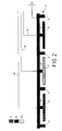
- Figure 2 shows a cross sectional view of the target as part of the apparatus of Figure 1.
- Figure 3 shows a plan view of the target shown in Figure 2.
- FIG. 1 With reference to the drawings and in particular to Figure 1, there is shown a vacuum chamber 1 having fixed therein a target generally shown at 2 and described in more detail below with reference to Figure 2 and 3.
- the chamber 1 is adapted to allow the passage of a substrate 3 through the chamber in a substantially horizontal plane in the direction indicated by the arrow A and in particular to pass beneath the lower surface of the target 2.
- the substrate may be a continuous one or may alternatively comprise a number of individual substrates passing through the chamber in succession.
- a number of optical emission sensors S each having a sensor head H are positioned between the target 2 and the substrate 3 such that the sensor heads 5 are close to the upper surface of the substrate whilst coating is taking place.
- the target 2 comprises an upper frame 4 of substantially rectangular cross section and made of metal, for example steel, stainless steel or aluminium, from which depends a flange structure whose component flanges 5 define nine rectangular cavities on the lower side of the upper frame 4.
- each cavity is positioned a plate 6, 7, 8, 9, 10, 11, 12, 13, 14 made from a substance being a component (or components) of the desired coating on the substrate.
- the individual plates are held in position and electrically insulated from the upper frame 4 by means of rods 15 of insulating material.
- the plates 6,10 and 14 could be made of chromium, plates 7,11,12 could be made of platinum and the plates 8, 9, 13 could be made of cobalt.
- Individual electrical connections 16 are made to each of the nine plates via leads passing through the insulating rods 15 to enable a variable electrical charge to be effected to each plate independently of the other plates.
- argon gas is introduced in to the chamber which had previously been evacuated down to for example 1 x 10 -3 or lower, mbar and an argon ion plasma formed in situ through the charging of the target.
- the plates 6 to 14 are individually charged, initially at substantial the same size of electric charge and a substrate 3 or substrates passed under the target in the direction of the arrow A such that the upper surface of the substrate 3 and the lower surfaces of the plates 6 to 14 are substantially parallel but spaced apart in the usual way.
- the sensor heads 5 Interposed between the substrate 3 and the target 4 are the sensor heads 5 which can sense the amount of the individual species present close to the surface of the substrate 3 as they pass from plates 6 to 14 to the upper surface of the substrate 3
- Means are provided to link the sensors' output to the electrical connections 16 such that the size of the electron charge on each plate, or alternating on each set of plate of the same composition, is varied when the sensors indicate a change in the amounts of the species approaching the substrate away from a desired, predetermined composition.
- the invention may also be used such that the composition of coating across the substrate surface varies by applying different electrical charges to different plates across the surface of the target.
- the substrate 3 may be held stationary relative to the target 2.
Landscapes
- Chemical & Material Sciences (AREA)
- Chemical Kinetics & Catalysis (AREA)
- Engineering & Computer Science (AREA)
- Materials Engineering (AREA)
- Mechanical Engineering (AREA)
- Metallurgy (AREA)
- Organic Chemistry (AREA)
- Physical Vapour Deposition (AREA)
- Physical Deposition Of Substances That Are Components Of Semiconductor Devices (AREA)
Applications Claiming Priority (2)
| Application Number | Priority Date | Filing Date | Title |
|---|---|---|---|
| GB9622913 | 1996-11-04 | ||
| GBGB9622913.3A GB9622913D0 (en) | 1996-11-04 | 1996-11-04 | Sputtering processes and apparatus |
Publications (1)
| Publication Number | Publication Date |
|---|---|
| EP0839926A1 true EP0839926A1 (de) | 1998-05-06 |
Family
ID=10802401
Family Applications (1)
| Application Number | Title | Priority Date | Filing Date |
|---|---|---|---|
| EP97308716A Withdrawn EP0839926A1 (de) | 1996-11-04 | 1997-10-30 | Sputterverfahren und -anlage |
Country Status (3)
| Country | Link |
|---|---|
| EP (1) | EP0839926A1 (de) |
| JP (1) | JPH10212572A (de) |
| GB (1) | GB9622913D0 (de) |
Citations (4)
| Publication number | Priority date | Publication date | Assignee | Title |
|---|---|---|---|---|
| GB1186669A (en) * | 1968-01-11 | 1970-04-02 | Ibm | Improvements relating to Target Electrodes for Sputtering Apparatus |
| JPS5989768A (ja) * | 1982-11-12 | 1984-05-24 | Fujitsu Ltd | 薄膜の形成方法 |
| FR2573441A1 (fr) * | 1984-11-19 | 1986-05-23 | Cit Alcatel | Cathode-cible pour depot, par pulverisation, d'un materiau composite sur un substrat |
| JPS62161957A (ja) * | 1986-01-10 | 1987-07-17 | Matsushita Electric Ind Co Ltd | スパツタリング装置 |
-
1996
- 1996-11-04 GB GBGB9622913.3A patent/GB9622913D0/en active Pending
-
1997
- 1997-10-30 EP EP97308716A patent/EP0839926A1/de not_active Withdrawn
- 1997-11-04 JP JP30184297A patent/JPH10212572A/ja active Pending
Patent Citations (4)
| Publication number | Priority date | Publication date | Assignee | Title |
|---|---|---|---|---|
| GB1186669A (en) * | 1968-01-11 | 1970-04-02 | Ibm | Improvements relating to Target Electrodes for Sputtering Apparatus |
| JPS5989768A (ja) * | 1982-11-12 | 1984-05-24 | Fujitsu Ltd | 薄膜の形成方法 |
| FR2573441A1 (fr) * | 1984-11-19 | 1986-05-23 | Cit Alcatel | Cathode-cible pour depot, par pulverisation, d'un materiau composite sur un substrat |
| JPS62161957A (ja) * | 1986-01-10 | 1987-07-17 | Matsushita Electric Ind Co Ltd | スパツタリング装置 |
Non-Patent Citations (2)
| Title |
|---|
| PATENT ABSTRACTS OF JAPAN vol. 008, no. 199 (C - 242) 12 September 1984 (1984-09-12) * |
| PATENT ABSTRACTS OF JAPAN vol. 012, no. 005 (C - 467) 8 January 1988 (1988-01-08) * |
Also Published As
| Publication number | Publication date |
|---|---|
| GB9622913D0 (en) | 1997-01-08 |
| JPH10212572A (ja) | 1998-08-11 |
Similar Documents
| Publication | Publication Date | Title |
|---|---|---|
| US6113752A (en) | Method and device for coating substrate | |
| US5215638A (en) | Rotating magnetron cathode and method for the use thereof | |
| US4946576A (en) | Apparatus for the application of thin layers to a substrate | |
| EP0537011B1 (de) | Zerstäubungsanlage | |
| US6284106B1 (en) | Method of producing flat panels | |
| US3756193A (en) | Coating apparatus | |
| US4992153A (en) | Sputter-CVD process for at least partially coating a workpiece | |
| US5346600A (en) | Plasma-enhanced magnetron-sputtered deposition of materials | |
| US4981566A (en) | Arrangement for measuring the thickness of thin layers | |
| US5382339A (en) | Shield and collimator pasting deposition chamber with a side pocket for pasting the bottom of the collimator | |
| EP0638659A2 (de) | Aufstäube-Beschichtungs-Target und Verfahren des Gebrauchs | |
| WO1992001081A1 (en) | Method and apparatus for co-sputtering and cross-sputtering homogeneous films | |
| EP0335526A3 (de) | Magnetron mit schaltbarem magnetischem Fluss und Betriebsverfahren | |
| JPH0768613B2 (ja) | 液状物質のスパッタ蒸着方法 | |
| US8652310B2 (en) | Trim magnets to adjust erosion rate of cylindrical sputter targets | |
| US6171659B1 (en) | Process for the formation of a coating on a substrate and device for the use this process | |
| US11674213B2 (en) | Sputtering apparatus including gas distribution system | |
| CN101368260A (zh) | 用于在基底上沉积涂层的方法和设备 | |
| US5407548A (en) | Method for coating a substrate of low resistance to corrosion | |
| EP0318441B1 (de) | Anlage und Verfahren zur Ablagerung einer dünnen Schicht auf ein durchsichtiges Substrat, insbesondere zur Herstellung von Glasscheiben | |
| EP0537012A1 (de) | Zerstäubungsanlage und -verfahren | |
| JP3439993B2 (ja) | マグネトロンスパッタ装置 | |
| JPH10212572A (ja) | スパッタリング方法および装置 | |
| JP2001115259A (ja) | マグネトロンスパッタ装置 | |
| JPH06340967A (ja) | 蒸着装置 |
Legal Events
| Date | Code | Title | Description |
|---|---|---|---|
| PUAI | Public reference made under article 153(3) epc to a published international application that has entered the european phase |
Free format text: ORIGINAL CODE: 0009012 |
|
| AK | Designated contracting states |
Kind code of ref document: A1 Designated state(s): CH DE FR GB IE IT LI |
|
| AX | Request for extension of the european patent |
Free format text: AL;LT;LV;RO;SI |
|
| 17P | Request for examination filed |
Effective date: 19980518 |
|
| AKX | Designation fees paid |
Free format text: AT BE CH DE DK LI |
|
| RBV | Designated contracting states (corrected) |
Designated state(s): AT BE CH DE DK LI |
|
| RBV | Designated contracting states (corrected) |
Designated state(s): AT BE CH DE DK IE LI |
|
| RBV | Designated contracting states (corrected) |
Designated state(s): CH DE FR GB IE IT LI |
|
| STAA | Information on the status of an ep patent application or granted ep patent |
Free format text: STATUS: THE APPLICATION IS DEEMED TO BE WITHDRAWN |
|
| 18D | Application deemed to be withdrawn |
Effective date: 20000501 |