EP0840227B1 - Procédé et dispositif pour déterminer le courant de repos - Google Patents
Procédé et dispositif pour déterminer le courant de repos Download PDFInfo
- Publication number
- EP0840227B1 EP0840227B1 EP97307939A EP97307939A EP0840227B1 EP 0840227 B1 EP0840227 B1 EP 0840227B1 EP 97307939 A EP97307939 A EP 97307939A EP 97307939 A EP97307939 A EP 97307939A EP 0840227 B1 EP0840227 B1 EP 0840227B1
- Authority
- EP
- European Patent Office
- Prior art keywords
- iddq
- switch
- value
- magnitude
- signal
- Prior art date
- Legal status (The legal status is an assumption and is not a legal conclusion. Google has not performed a legal analysis and makes no representation as to the accuracy of the status listed.)
- Expired - Lifetime
Links
- 238000000034 method Methods 0.000 title claims description 26
- 238000012360 testing method Methods 0.000 claims description 90
- 238000005070 sampling Methods 0.000 claims description 4
- 230000004044 response Effects 0.000 claims description 3
- 230000000737 periodic effect Effects 0.000 claims 7
- 230000008878 coupling Effects 0.000 claims 2
- 238000010168 coupling process Methods 0.000 claims 2
- 238000005859 coupling reaction Methods 0.000 claims 2
- 238000005259 measurement Methods 0.000 description 12
- 239000003990 capacitor Substances 0.000 description 9
- 238000004364 calculation method Methods 0.000 description 8
- 230000003071 parasitic effect Effects 0.000 description 7
- 238000004458 analytical method Methods 0.000 description 5
- 230000007547 defect Effects 0.000 description 5
- 238000004519 manufacturing process Methods 0.000 description 5
- 230000000153 supplemental effect Effects 0.000 description 5
- 238000010586 diagram Methods 0.000 description 4
- 238000011156 evaluation Methods 0.000 description 2
- 230000003068 static effect Effects 0.000 description 2
- 230000003321 amplification Effects 0.000 description 1
- 238000013459 approach Methods 0.000 description 1
- 230000003139 buffering effect Effects 0.000 description 1
- 238000012512 characterization method Methods 0.000 description 1
- 230000001276 controlling effect Effects 0.000 description 1
- 230000002596 correlated effect Effects 0.000 description 1
- 230000000875 corresponding effect Effects 0.000 description 1
- 230000002950 deficient Effects 0.000 description 1
- 238000013461 design Methods 0.000 description 1
- 230000005669 field effect Effects 0.000 description 1
- 238000002955 isolation Methods 0.000 description 1
- 238000003199 nucleic acid amplification method Methods 0.000 description 1
- 238000012545 processing Methods 0.000 description 1
Images


Classifications
-
- G—PHYSICS
- G01—MEASURING; TESTING
- G01R—MEASURING ELECTRIC VARIABLES; MEASURING MAGNETIC VARIABLES
- G01R31/00—Arrangements for testing electric properties; Arrangements for locating electric faults; Arrangements for electrical testing characterised by what is being tested not provided for elsewhere
- G01R31/28—Testing of electronic circuits, e.g. by signal tracer
- G01R31/30—Marginal testing, e.g. by varying supply voltage
- G01R31/3004—Current or voltage test
- G01R31/3008—Quiescent current [IDDQ] test or leakage current test
-
- G—PHYSICS
- G01—MEASURING; TESTING
- G01R—MEASURING ELECTRIC VARIABLES; MEASURING MAGNETIC VARIABLES
- G01R31/00—Arrangements for testing electric properties; Arrangements for locating electric faults; Arrangements for electrical testing characterised by what is being tested not provided for elsewhere
- G01R31/28—Testing of electronic circuits, e.g. by signal tracer
- G01R31/30—Marginal testing, e.g. by varying supply voltage
- G01R31/3004—Current or voltage test
-
- G—PHYSICS
- G01—MEASURING; TESTING
- G01R—MEASURING ELECTRIC VARIABLES; MEASURING MAGNETIC VARIABLES
- G01R31/00—Arrangements for testing electric properties; Arrangements for locating electric faults; Arrangements for electrical testing characterised by what is being tested not provided for elsewhere
- G01R31/28—Testing of electronic circuits, e.g. by signal tracer
- G01R31/317—Testing of digital circuits
- G01R31/3181—Functional testing
- G01R31/319—Tester hardware, i.e. output processing circuits
- G01R31/3193—Tester hardware, i.e. output processing circuits with comparison between actual response and known fault free response
Definitions
- the present invention is generally related to the testing of integrated circuits and more particularly related to the rapid functional testing and evaluation of the quality and current leakage of digital CMOS integrated circuits.
- Integrated circuits are regularly subjected to quality checks and performance evaluations following their manufacture. Since the quantity of devices is substantial, the testing is performed by automated equipment which has been optimized for throughput and accuracy. Examples of automated test equipment for IC manufacture are an HP83000 model F330 Digital IC Test System, available from Hewlett Packard Company and an S9000 Test System, models MX or FX available from Schlumberger, Inc. Generally, these types of test equipment are configured as shown in FIG. 1, in which the IC Test System 101 is coupled to a workstation 103 (or similar computer interface for automated programming of the IC Test System) and accepts an IC device under test (DUT) 105.
- a workstation 103 or similar computer interface for automated programming of the IC Test System
- the DUT can be an individual packaged IC or a wafer containing a multitude of IC dice or any stage of process between the two.
- a dedicated mainframe controller 107 controls the preprogrammed operations of the test equipment and directs a DUT Interface 109 to configure its resident hardware to source or receive signals to/from the DUT 105.
- Electrical and mechanical interconnection and attachment for the duration of the testing process is achieved by a DUT Interconnect board 111, which typically has 100 to 400 connection pins to temporarily connect to the pads or package pins of the DUT 105.
- the DUT 105 Since the DUT 105 is usually a digital device, a number of the DUT inputs are forced to logic levels established by the controlling program of the mainframe 107 during testing. Other of the IC outputs are monitored for the resulting logic level produced by the DUT in response to the forced logic levels. A determination of the logic state of the monitored outputs is made by the DUT Interface 109 and the results are analyzed and reported as pass/fail by the mainframe 107. Depending upon the test desired by the engineer, the test program can sequence through a number of cycles to test the operating performance of the DUT or to test static parameters of particular portions of the DUT.
- IDDQ quiescent current drain
- One or more IDDQ monitors may be designed onto the DUT Interconnect 111 or designed into the circuitry of the IC to detect leakage of portions of the IC digital circuitry and to provide an overcurrent error when the quiescent current exceeds a predetermined value. See, for example, U.S. Patent Application No. (docket no. 10960006), “Multiple On-Chip IDDQ Monitors", filed on October 16, 1996, on behalf of Charles Allen Brown, and assigned to the assignee of the present invention. It has also been suggested (see, Keating et al., "A New Approach To Dynamic IDD Testing", Proc.
- Keating/Meyer circuit be used to test leakage of Ics.
- a Keating/Wallquist circuit Such a test configuration will be called a Keating/Wallquist circuit hereinafter.
- a Keating/Wallquist circuit is shown in the diagram of FIG.
- the intrinsic capacitance 205 of the DUT 105, the parasitic capacitance 207 of the interconnect to the DUT, and, perhaps, purposefully added capacitance (not shown) stores enough electric charge to maintain a voltage across the quiescent DUT. This voltage is monitored at the DUT for a decay in voltage magnitude as the internal impedance of the DUT IC bleeds off the charge. A defective IC (or an IC of marginal quality) experiences a relatively rapid decay of voltage while a good IC demonstrates relatively slow decay of voltage.
- a preferred embodiment of the present invention employs an Hewlett-Packard Company HP83000 test system to accomplish rapid testing of CMOS integrated circuits.
- the preferred embodiment employs a version of a Keating/Wallquist circuit suitable to the present invention to sense the quiescent leakage current (IDDQ) of a CMOS logic circuit.
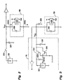
- the schematic of FIG. 3 illustrates the connection of the Keating/Wallquist circuit in the preferred embodiment.
- a power supply 301 provides operating power for the device under test 105 and samples the voltage V DD at the DUT. This sample is returned as a sense voltage to the power supply 301 by way of a sense line.
- a resistor 303 provides a coarse feedback to the sense line during periods when a V DD sample is not being returned to the power supply 301.
- Two field effect transistors 304 and 305 are located . on the DUT Interconnect 111.
- Transistor 304 is connected in series with the power supply 301 and couples power to the device under test 105. This supplied power also charges a parasitic capacitor 309, a supplemental capacitor 307, and an intrinsic capacitor 205 of the device under test.
- the separate V DD sense line is returned to the power supply 301 via the series-coupled transistor 305.
- a signal is coupled to the gate of transistors 304 and 305 simultaneously so that both transistors are turned off. This switching of the transistors causes the cessation of supplying voltage to the DUT 105 and the disconnection of the sense voltage being returned to the power supply 301, respectively. It is a feature of the present invention that two switches, one in the power supply and one in the voltage sense return, are employed in an IDDQ test to provide a more accurate control of V DD when the transistors 304 and 305 are in the on state.
- the power decay signal represented by the supply voltage, V DD , applied to the device under test 105 is determined by the charge remaining in the parasitic capacitor 309, a supplemental capacitor 307 which may be added for ease of measurement, and the intrinsic capacitor 205.
- V DD supply voltage
- the logic of the device under test 105 is placed in a predetermined but unclocked and quiescent state or set of states, such that only the DUT leakage current is being drawn.
- this leakage current is drawn by the expected channel resistance (R C ), which is an unavoidable impedance related to the number of gates in the logic circuit and the particular processes used in the manufacture of the circuit, and a defect resistance (R D ) which is indicative of an undesirable defect such as gate oxide shorts.
- R C expected channel resistance
- R D defect resistance
- conventional integrated circuit automated test equipment is designed for rapid pass/fail indications and is not generally equipped to provide analytical data such as an analysis of an RC time constant voltage decay. It is a feature of the present invention, however, that recognition of a detected pass/fail event (which may be a pass/fail test separate and independent of an IDDQ pass/fail test) following a predetermined number of test cycles can be processed to yield an approximation of the voltage decay waveform and from this approximation the IDDQ current value can be determined.
- one or more of the tests programmed to be performed by the HP83000 test system is that of an IDDQ pass/fail.
- test system is programmed to test for IDDQ pass/fail over a sequential number of cycles, each cycle equaling a predetermined amount of time (for example, in the preferred embodiment approximately 5 microseconds). It should be noted that since the test system can test in excess of 100 DUT test points at a given time, that an IDDQ and other leakage current measurements can be performed at the same time as other DUT parameters are measured. Nevertheless, the following discussion considers the measurement of leakage current in isolation but other measurements, including other IDDQ measurements, can be made at the same time.
- the mainframe 107 is preprogrammed to test the drooping V DD in a succession of tester cycles.
- the test sample times are predetermined and downloaded from the workstation 103 to the mainframe 107.
- the decaying V DD drops below a selected threshold, a failure is indicated starting at one of the test sample times.
- Leakage current is tested following the placing of the DUT in an appropriate low power or quiescent state.
- a value of IDDQ leakage current is determined independently from a determination of IDDQ pass/fail while employing a pass/fail series of tests; that is, a DUT may not fail the conventional IDDQ test but its IDDQ value can be determined by continuing the sampling of the decaying V DD until it drops below another predetermined voltage threshold for which IDDQ characteristics are known.
- These characteristics can be DUT 105 and DUT Interconnect 111 resistances and capacitances which have been previously determined from prior measurement and device samples at the predetermined voltage threshold. These characteristics can also be a measured family of V DD decay voltage curves which have been previously correlated to specific IDDQ current values. Either IDDQ determination method may be employed in alternate embodiments.
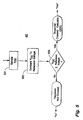
- the program When an IDDQ determination is to be performed, the program experiences a pointer, 401, from the workstation 103 to the test process which defines, among other things, the IDDQ test.
- the process may be distributed between the workstation 103, the mainframe 107, and the DUT Interface 109 as the designer deems most optimum.
- the preferred embodiment assigns calculation steps to the workstation. Since this particular IDDQ test is likely to be one of many IDDQ tests to be run by the entire test suite of the test system, a V DD threshold limit is set at step 403. It should be noted that this limit can be (and in the preferred embodiment is) different from a limit equated to a determination of a failed DUT due to an excessive IDDQ value.
- Transistors 304 and 305 are placed in the off(open) state at step 413.
- a determination of whether the conventionally established IDDQ device failure current is made at steps 414, 415, and 416.
- a determination of whether the previously established V DD threshold has been crossed is made at a comparison step 417. Since the R C time constant is related to IDDQ, a selected voltage after a given amount of time can be related to the leakage current of the DUT.
- the comparison step 417 employed in the preferred embodiment is shown in FIG. 5.
- the V DD voltage magnitude is sampled at step 501.
- a V DD magnitude greater than the threshold voltage magnitude does not trigger a calculation of IDDQ while a measured V DD less than the threshold voltage magnitude initiates the calculation of IDDQ.
- This comparison and determination is shown in steps 503 and 505. While a pass/fail result is obtained, a further process yields a value for IDDQ. If the result from the comparison step 417 shows that the threshold voltage has not been crossed ("N"), the process moves to step 419 to allow other pass/fail tests to be performed during the present test cycle. If the leakage current test process is complete, the mainframe will progress to another series of programmed test. If not, the next test cycle is awaited and another threshold limit test is made at step 417.
- step 417 If the threshold voltage has been crossed ("V") at step 417, a calculation of the time to such crossing is made at step 423. A count of the number of test cycles, N, since the opening of the switch is made at step 421. The length of the period, L, is multiplied by the number of test cycles to yield a total time, t.
- dV dt ⁇ ⁇ V ⁇ t and ⁇ t is a result of the calculation of step 423.
- the total shunt capacitance can be made significantly larger than the intrinsic capacitance: C D ⁇ C
- a family of decaying residual DUT voltage curves related to time and derived from previous measurements of sampled DUTs (with known values of shunt capacitance) is stored in a memory which may be part of the mainframe 107 or the workstation 103.
- a measured value of voltage is provided from a sample
- the time relating to each of the decaying residual voltage signals at this sample voltage are returned from the memory at step 601 of FIG. 6.
- the recalled time values are compared, at step 603, to the time to threshold crossing which was calculated at step 423.
- the related residual voltage curve for which the recalled time value is found closest to the actual sampled time period is deemed representative of the residual voltage decay waveform, at step 605.
- the IDDQ value which is related to the representative residual voltage curve is selected as the actual IDDQ value at step 607.
- a family of decaying residual voltage curves is shown for IDDQ values of 64 ⁇ A, 32 ⁇ A, 16 ⁇ A, 8 ⁇ A, 1 ⁇ A, and open socket (no DUT installed in the DUT Interconnect 111).
- V DD 3.30 volts
- the memory returns the values of time corresponding to each residual voltage curve, ie, 50 ⁇ sec for the 64 ⁇ A curve, 75 ⁇ sec for the 32 ⁇ A curve, 100 ⁇ sec for the 16 ⁇ A curve, etc. If the time elapsed, based upon the number of test cycles, is 100 ⁇ sec, the present invention deems the value of IDDQ to be 16 ⁇ A and this is the value provided for IDDQ analysis.
Landscapes
- Engineering & Computer Science (AREA)
- General Engineering & Computer Science (AREA)
- Physics & Mathematics (AREA)
- General Physics & Mathematics (AREA)
- Tests Of Electronic Circuits (AREA)
- Testing Of Individual Semiconductor Devices (AREA)
- Metal-Oxide And Bipolar Metal-Oxide Semiconductor Integrated Circuits (AREA)
- Testing Or Measuring Of Semiconductors Or The Like (AREA)
Claims (10)
- Un appareil de détermination d'une valeur de IDDQ d'un dispositif en cours de test comprenant:une alimentation en énergie (201) dont une sortie d'alimentation en énergie alimente en énergie ledit dispositif en cours de test (105);un premier commutateur qui couple, lorsqu'il est fermé, ladite sortie d'alimentation en énergie audit dispositif en cours de test;une sortie de signal de contrôleur, couplée au dispositif en cours de test, grâce à quoi un signal de tension est contrôlé; etau moins un processeur (107) qui ouvre ledit premier commutateur et échantillonne ensuite périodiquement ledit signal de tension à ladite sortie de signal de contrôleur, compare l'amplitude dudit signal de tension lors de chaque échantillon périodique à une amplitude de signal de référence prédéterminé, indique un croisement de seuil lorsque ladite comparaison indique une amplitude dudit signal de tension inférieure à ladite amplitude de signal de référence et, en réponse à l'indication du croisement de seuil, calcule la valeur de IDDQ sur la base du nombre d'échantillons périodiques à partir de ladite ouverture dudit premier commutateur et dudit signal de tension.
- Un appareil de détermination d'une valeur d'IDDQ selon la revendication 1, qui comprend en outre une entrée de signal de détection à ladite alimentation en énergie et un deuxième commutateur (305) couplé, lorsqu'il est fermé, au dispositif en cours de test et à ladite entrée de signal de détection de ladite alimentation en énergie et répondant audit processeur pour s'ouvrir lors de l'ouverture dudit premier commutateur.
- Un appareil de détermination d'une valeur d'IDDQ selon la revendication 1, dans lequel ledit processeur unique au moins comprend en outre une mémoire pour enregistrer au moins une relation de signal de tension en fonction du temps associée à une valeur d'IDDQ.
- Un appareil de détermination d'une valeur d'IDDQ selon la revendication 2, dans lequel lesdits premier et deuxième commutateurs comprennent en outre chacun un transistor et dans lequel une grille de chacun desdits transistors est connectée à l'autre.
- Un appareil de détermination d'une valeur d'IDDQ selon la revendication 1 dans lequel ledit signal de tension comprend en outre une tension.
- Un processus de détermination d'une valeur d'IDDQ d'un dispositif en cours de test (105) qui comprend les étapes consistant à:envoyer à partir d'une alimentation en énergie (201) un signal de sortie d'alimentation en énergie;coupler ledit signal de sortie en alimentation en énergie au dispositif en cours de test par l'intermédiaire d'un premier commutateur (304);ouvrir (413) ledit premier commutateur en déconnectant ainsi du dispositif en cours de test ledit signal de sortie d'alimentation en énergie;échantillonner périodiquement (501) l'amplitude d'un signal de tension indicatif d'une décroissance de tension dudit dispositif en cours de test après l'ouverture dudit premier commutateur;comparer (503) au moins l'une desdites amplitudes de signaux de tension échantillonnés à une amplitude d'un signal de référence prédéterminé;indiquer (505) un croisement de seuil lorsque ladite étape de comparaison indique une amplitude du signal de tension inférieure à ladite amplitude du signal de référence; etcalculer la valeur d'IDDQ en réponse audit croisement de seuil, sur la base du nombre d'échantillons périodiques à partir de l'ouverture dudit premier commutateur et dudit signal de tension.
- Un procédé selon la revendication 6 dans lequel ladite étape de calcul comprend en outre les étapes consistant à:déterminer (405) le laps de temps entre chaque échantillonnage périodique;compter (421) le nombre d'échantillons périodiques qui se produisent à partir de l'instant qui suit l'ouverture dudit premier commutateur; etmultiplier ledit laps de temps entre chaque échantillonnage périodique par le nombre compté d'échantillons périodiques pour obtenir (423) l'amplitude du laps de temps total à partir de ladite ouverture dudit premier commutateur et de ladite indication du croisement de seuil.
- Un procédé selon la revendication 7 dans lequel ladite étape de calcul de la valeur d'IDDQ comprend en outre les étapes consistant à:obtenir (407) une première amplitude dudit signal de tension avant ladite ouverture dudit premier commutateur;déterminer (409) une ampleur de capacité montée en shunt au dispositif en cours de test lorsque ledit premier commutateur est ouvert;calculer une différence entre ladite première amplitude et au moins une amplitude dudit signal de tension échantillonné périodiquement;multiplier ladite différence calculée par ladite quantité déterminée de capacité et diviser par ladite amplitude du laps de temps total en établissant ainsi un premier courant; etcombiner ledit premier courant avec le courant tiré par la résistance de canal du dispositif en cours de test.
- Un procédé selon la revendication 7 dans lequel ladite étape de calcul de la valeur d'IDDQ comprend en outre les étapes consistant à:pour ladite amplitude échantillonnée dudit signal de tension, rappeler (601) d'une mémoire au moins une valeur de temps de la courbe du signal de tension et une valeur associée d'IDDQ d'une série de valeurs enregistrées valeur de temps de la courbe de décroissance de tension et de valeurs associées d'IDDQ;comparer (603) ladite valeur de temps rappelée audit laps de temps total;déterminer (607) comme dite valeur d'IDDQ ladite valeur d'IDDQ associée lorsque ladite étape de comparaison indique que ladite valeur de temps rappelée de la courbe de tension est plus proche d'être égale audit laps de temps total que toute autre de ladite série de valeurs enregistrées de temps de la courbe de tension.
- Un procédé selon la revendication 6 qui comprend en outre les étapes consistant à:coupler un signal de détection égal audit signal de sortie d'alimentation en énergie à une entrée de détection de ladite alimentation en énergie par l'intermédiaire d'un deuxième commutateur (305); etouvrir ledit deuxième commutateur de façon essentiellement simultanée avec ledit premier commutateur en déconnectant ainsi de ladite alimentation en énergie ledit signal de détection.
Applications Claiming Priority (2)
| Application Number | Priority Date | Filing Date | Title |
|---|---|---|---|
| US08/741,879 US5789933A (en) | 1996-10-30 | 1996-10-30 | Method and apparatus for determining IDDQ |
| US741879 | 2003-12-19 |
Publications (2)
| Publication Number | Publication Date |
|---|---|
| EP0840227A1 EP0840227A1 (fr) | 1998-05-06 |
| EP0840227B1 true EP0840227B1 (fr) | 2002-03-06 |
Family
ID=24982592
Family Applications (1)
| Application Number | Title | Priority Date | Filing Date |
|---|---|---|---|
| EP97307939A Expired - Lifetime EP0840227B1 (fr) | 1996-10-30 | 1997-10-08 | Procédé et dispositif pour déterminer le courant de repos |
Country Status (4)
| Country | Link |
|---|---|
| US (1) | US5789933A (fr) |
| EP (1) | EP0840227B1 (fr) |
| JP (1) | JP2983938B2 (fr) |
| DE (1) | DE69710842T2 (fr) |
Families Citing this family (20)
| Publication number | Priority date | Publication date | Assignee | Title |
|---|---|---|---|---|
| US6087843A (en) * | 1997-07-14 | 2000-07-11 | Credence Systems Corporation | Integrated circuit tester with test head including regulating capacitor |
| DE19836361C1 (de) * | 1998-08-11 | 2000-03-30 | Siemens Ag | Verfahren zur Leckstromprüfung einer Kontaktierungsstelle einer integrierten Schaltung |
| US6366108B2 (en) | 1998-12-01 | 2002-04-02 | Agilent Technologies, Inc. | System and method for detecting defects within an electrical circuit by analyzing quiescent current |
| US6307376B1 (en) | 1998-12-23 | 2001-10-23 | Eaton Corporation | Fault detection system and method for solenoid controlled actuators of a transmission system |
| DE69926126T2 (de) * | 1999-09-14 | 2006-05-11 | Stmicroelectronics S.R.L., Agrate Brianza | Verfahren zur ruhestrombestimmung |
| US6810344B1 (en) * | 1999-11-11 | 2004-10-26 | Kabushiki Kaisha Toshiba | Semiconductor testing method and semiconductor testing apparatus for semiconductor devices, and program for executing semiconductor testing method |
| US6342790B1 (en) | 2000-04-13 | 2002-01-29 | Pmc-Sierra, Inc. | High-speed, adaptive IDDQ measurement |
| US6535005B1 (en) * | 2000-04-26 | 2003-03-18 | Emc Corporation | Systems and methods for obtaining an electrical characteristics of a circuit board assembly process |
| US6586921B1 (en) | 2000-05-12 | 2003-07-01 | Logicvision, Inc. | Method and circuit for testing DC parameters of circuit input and output nodes |
| US6693439B1 (en) | 2000-09-28 | 2004-02-17 | Cadence Design Systems, Inc. | Apparatus and methods for measuring noise in a device |
| US6542385B1 (en) | 2000-11-22 | 2003-04-01 | Teradyne, Inc. | DUT power supply having improved switching DC-DC converter |
| US6556034B1 (en) | 2000-11-22 | 2003-04-29 | Teradyne, Inc. | High speed and high accuracy DUT power supply with active boost circuitry |
| US6448748B1 (en) | 2001-03-01 | 2002-09-10 | Teradyne, Inc. | High current and high accuracy linear amplifier |
| US6623992B1 (en) * | 2002-03-08 | 2003-09-23 | Lsi Logic Corporation | System and method for determining a subthreshold leakage test limit of an integrated circuit |
| DE60307297T2 (de) * | 2002-09-20 | 2007-10-18 | Koninklijke Philips Electronics N.V. | Verfahren und einrichtung zur ruhestrombestimmung |
| KR100496861B1 (ko) * | 2002-09-26 | 2005-06-22 | 삼성전자주식회사 | 하나의 핸들러에 2개 이상의 테스트 보드를 갖는 테스트장비 및 그 테스트 방법 |
| EP2064562B1 (fr) * | 2006-09-06 | 2010-04-21 | Nxp B.V. | Circuit intégré pouvant etre testé et procédé de test de ci |
| US8526252B2 (en) * | 2009-03-17 | 2013-09-03 | Seagate Technology Llc | Quiescent testing of non-volatile memory array |
| US9324822B2 (en) * | 2014-07-01 | 2016-04-26 | Globalfoundries Inc. | Gate dielectric protection for transistors |
| US11599098B2 (en) | 2019-05-08 | 2023-03-07 | Ares Technologies, Inc. | Apparatus and methods for testing circuit elements at one or more manufacturing stages |
Family Cites Families (3)
| Publication number | Priority date | Publication date | Assignee | Title |
|---|---|---|---|---|
| GB2285516B (en) * | 1994-01-05 | 1997-07-30 | Hewlett Packard Co | Quiescent current testing of dynamic logic systems |
| US5552744A (en) * | 1994-08-11 | 1996-09-03 | Ltx Corporation | High speed IDDQ monitor circuit |
| US5519333A (en) * | 1994-09-09 | 1996-05-21 | Sandia Corporation | Elevated voltage level IDDQ failure testing of integrated circuits |
-
1996
- 1996-10-30 US US08/741,879 patent/US5789933A/en not_active Expired - Fee Related
-
1997
- 1997-10-08 EP EP97307939A patent/EP0840227B1/fr not_active Expired - Lifetime
- 1997-10-08 DE DE69710842T patent/DE69710842T2/de not_active Expired - Fee Related
- 1997-10-13 JP JP9278916A patent/JP2983938B2/ja not_active Expired - Fee Related
Also Published As
| Publication number | Publication date |
|---|---|
| JP2983938B2 (ja) | 1999-11-29 |
| DE69710842D1 (de) | 2002-04-11 |
| JPH10142288A (ja) | 1998-05-29 |
| US5789933A (en) | 1998-08-04 |
| EP0840227A1 (fr) | 1998-05-06 |
| DE69710842T2 (de) | 2002-08-29 |
Similar Documents
| Publication | Publication Date | Title |
|---|---|---|
| EP0840227B1 (fr) | Procédé et dispositif pour déterminer le courant de repos | |
| US6291978B1 (en) | System and method for detecting shorts, opens and connected pins on a printed circuit board using automatic test equipment | |
| US7663382B2 (en) | High-speed capacitor leakage measurement systems and methods | |
| US6586921B1 (en) | Method and circuit for testing DC parameters of circuit input and output nodes | |
| US7818137B2 (en) | Characterization circuit for fast determination of device capacitance variation | |
| US5371457A (en) | Method and apparatus to test for current in an integrated circuit | |
| US6828815B2 (en) | Method and apparatus for defect analysis of semiconductor integrated circuit | |
| KR100499849B1 (ko) | 반도체 테스트 시스템용 전원 전류 측정 유닛 | |
| KR19990082339A (ko) | 집적된 회로 장치 시험용 어셈블리 및 방법 | |
| US5552744A (en) | High speed IDDQ monitor circuit | |
| JPH0954140A (ja) | 半導体集積回路のテスト方法および装置 | |
| US6194911B1 (en) | Integrated circuit tester with compensation for leakage current | |
| US20240369614A1 (en) | Probe card for device under test | |
| US6930500B2 (en) | IDDQ testing of CMOS mixed-signal integrated circuits | |
| US20090093987A1 (en) | Method for accurate measuring stray capacitance of automatic test equipment and system thereof | |
| EP1635183B1 (fr) | Dispositif de surveillance du courant de repos d'un dispositif électronique | |
| US20040153276A1 (en) | Method and apparatus for reduced pin count package connection verification | |
| JPH03203250A (ja) | 集積回路用モニター装置及びモニター方法 | |
| JPH09101330A (ja) | プルアップ抵抗及びプルダウン抵抗の自動試験器 | |
| Keezer et al. | Improved sensitivity for parallel test of substrate interconnections | |
| JPS6262300B2 (fr) |
Legal Events
| Date | Code | Title | Description |
|---|---|---|---|
| PUAI | Public reference made under article 153(3) epc to a published international application that has entered the european phase |
Free format text: ORIGINAL CODE: 0009012 |
|
| AK | Designated contracting states |
Kind code of ref document: A1 Designated state(s): CH DE FR GB IT LI NL |
|
| AX | Request for extension of the european patent |
Free format text: AL;LT;LV;RO;SI |
|
| 17P | Request for examination filed |
Effective date: 19981016 |
|
| AKX | Designation fees paid |
Free format text: CH DE FR GB IT LI NL |
|
| RBV | Designated contracting states (corrected) |
Designated state(s): CH DE FR GB IT LI NL |
|
| 17Q | First examination report despatched |
Effective date: 20001221 |
|
| RAP1 | Party data changed (applicant data changed or rights of an application transferred) |
Owner name: HEWLETT-PACKARD COMPANY, A DELAWARE CORPORATION |
|
| RAP1 | Party data changed (applicant data changed or rights of an application transferred) |
Owner name: AGILENT TECHNOLOGIES, INC. |
|
| GRAG | Despatch of communication of intention to grant |
Free format text: ORIGINAL CODE: EPIDOS AGRA |
|
| RAP1 | Party data changed (applicant data changed or rights of an application transferred) |
Owner name: AGILENT TECHNOLOGIES INC. |
|
| RAP1 | Party data changed (applicant data changed or rights of an application transferred) |
Owner name: AGILENT TECHNOLOGIES INC. A DELAWARE CORPORATION |
|
| GRAG | Despatch of communication of intention to grant |
Free format text: ORIGINAL CODE: EPIDOS AGRA |
|
| GRAH | Despatch of communication of intention to grant a patent |
Free format text: ORIGINAL CODE: EPIDOS IGRA |
|
| GRAH | Despatch of communication of intention to grant a patent |
Free format text: ORIGINAL CODE: EPIDOS IGRA |
|
| RAP1 | Party data changed (applicant data changed or rights of an application transferred) |
Owner name: AGILENT TECHNOLOGIES, INC. (A DELAWARE CORPORATION |
|
| REG | Reference to a national code |
Ref country code: GB Ref legal event code: IF02 |
|
| GRAA | (expected) grant |
Free format text: ORIGINAL CODE: 0009210 |
|
| AK | Designated contracting states |
Kind code of ref document: B1 Designated state(s): CH DE FR GB IT LI NL |
|
| PG25 | Lapsed in a contracting state [announced via postgrant information from national office to epo] |
Ref country code: NL Free format text: LAPSE BECAUSE OF FAILURE TO SUBMIT A TRANSLATION OF THE DESCRIPTION OR TO PAY THE FEE WITHIN THE PRESCRIBED TIME-LIMIT Effective date: 20020306 Ref country code: LI Free format text: LAPSE BECAUSE OF FAILURE TO SUBMIT A TRANSLATION OF THE DESCRIPTION OR TO PAY THE FEE WITHIN THE PRESCRIBED TIME-LIMIT Effective date: 20020306 Ref country code: IT Free format text: LAPSE BECAUSE OF FAILURE TO SUBMIT A TRANSLATION OF THE DESCRIPTION OR TO PAY THE FEE WITHIN THE PRESCRIBED TIME-LIMIT;WARNING: LAPSES OF ITALIAN PATENTS WITH EFFECTIVE DATE BEFORE 2007 MAY HAVE OCCURRED AT ANY TIME BEFORE 2007. THE CORRECT EFFECTIVE DATE MAY BE DIFFERENT FROM THE ONE RECORDED. Effective date: 20020306 Ref country code: CH Free format text: LAPSE BECAUSE OF FAILURE TO SUBMIT A TRANSLATION OF THE DESCRIPTION OR TO PAY THE FEE WITHIN THE PRESCRIBED TIME-LIMIT Effective date: 20020306 |
|
| REG | Reference to a national code |
Ref country code: CH Ref legal event code: EP |
|
| REF | Corresponds to: |
Ref document number: 69710842 Country of ref document: DE Date of ref document: 20020411 |
|
| NLV1 | Nl: lapsed or annulled due to failure to fulfill the requirements of art. 29p and 29m of the patents act | ||
| ET | Fr: translation filed | ||
| REG | Reference to a national code |
Ref country code: CH Ref legal event code: PL |
|
| PLBE | No opposition filed within time limit |
Free format text: ORIGINAL CODE: 0009261 |
|
| STAA | Information on the status of an ep patent application or granted ep patent |
Free format text: STATUS: NO OPPOSITION FILED WITHIN TIME LIMIT |
|
| 26N | No opposition filed |
Effective date: 20021209 |
|
| PGFP | Annual fee paid to national office [announced via postgrant information from national office to epo] |
Ref country code: FR Payment date: 20041020 Year of fee payment: 8 |
|
| PG25 | Lapsed in a contracting state [announced via postgrant information from national office to epo] |
Ref country code: FR Free format text: LAPSE BECAUSE OF NON-PAYMENT OF DUE FEES Effective date: 20060630 |
|
| REG | Reference to a national code |
Ref country code: GB Ref legal event code: 732E |
|
| REG | Reference to a national code |
Ref country code: FR Ref legal event code: ST Effective date: 20060630 |
|
| PGFP | Annual fee paid to national office [announced via postgrant information from national office to epo] |
Ref country code: DE Payment date: 20081014 Year of fee payment: 12 |
|
| PGFP | Annual fee paid to national office [announced via postgrant information from national office to epo] |
Ref country code: GB Payment date: 20081008 Year of fee payment: 12 |
|
| PG25 | Lapsed in a contracting state [announced via postgrant information from national office to epo] |
Ref country code: DE Free format text: LAPSE BECAUSE OF NON-PAYMENT OF DUE FEES Effective date: 20100501 |
|
| PG25 | Lapsed in a contracting state [announced via postgrant information from national office to epo] |
Ref country code: GB Free format text: LAPSE BECAUSE OF NON-PAYMENT OF DUE FEES Effective date: 20091008 |