EP0840502A2 - Kompakte Digitalkamera mit segmentierten Blickfeldern - Google Patents
Kompakte Digitalkamera mit segmentierten Blickfeldern Download PDFInfo
- Publication number
- EP0840502A2 EP0840502A2 EP97203282A EP97203282A EP0840502A2 EP 0840502 A2 EP0840502 A2 EP 0840502A2 EP 97203282 A EP97203282 A EP 97203282A EP 97203282 A EP97203282 A EP 97203282A EP 0840502 A2 EP0840502 A2 EP 0840502A2
- Authority
- EP
- European Patent Office
- Prior art keywords
- sub
- lenslet
- array
- photodetectors
- image
- Prior art date
- Legal status (The legal status is an assumption and is not a legal conclusion. Google has not performed a legal analysis and makes no representation as to the accuracy of the status listed.)
- Withdrawn
Links
Images





Classifications
-
- G—PHYSICS
- G02—OPTICS
- G02B—OPTICAL ELEMENTS, SYSTEMS OR APPARATUS
- G02B3/00—Simple or compound lenses
- G02B3/0006—Arrays
- G02B3/0037—Arrays characterized by the distribution or form of lenses
- G02B3/0043—Inhomogeneous or irregular arrays, e.g. varying shape, size, height
-
- G—PHYSICS
- G02—OPTICS
- G02B—OPTICAL ELEMENTS, SYSTEMS OR APPARATUS
- G02B3/00—Simple or compound lenses
- G02B3/0006—Arrays
- G02B3/0037—Arrays characterized by the distribution or form of lenses
- G02B3/0056—Arrays characterized by the distribution or form of lenses arranged along two different directions in a plane, e.g. honeycomb arrangement of lenses
-
- H—ELECTRICITY
- H04—ELECTRIC COMMUNICATION TECHNIQUE
- H04N—PICTORIAL COMMUNICATION, e.g. TELEVISION
- H04N23/00—Cameras or camera modules comprising electronic image sensors; Control thereof
- H04N23/50—Constructional details
- H04N23/55—Optical parts specially adapted for electronic image sensors; Mounting thereof
-
- H—ELECTRICITY
- H04—ELECTRIC COMMUNICATION TECHNIQUE
- H04N—PICTORIAL COMMUNICATION, e.g. TELEVISION
- H04N25/00—Circuitry of solid-state image sensors [SSIS]; Control thereof
- H04N25/40—Extracting pixel data from image sensors by controlling scanning circuits, e.g. by modifying the number of pixels sampled or to be sampled
- H04N25/41—Extracting pixel data from a plurality of image sensors simultaneously picking up an image, e.g. for increasing the field of view by combining the outputs of a plurality of sensors
-
- H—ELECTRICITY
- H04—ELECTRIC COMMUNICATION TECHNIQUE
- H04N—PICTORIAL COMMUNICATION, e.g. TELEVISION
- H04N25/00—Circuitry of solid-state image sensors [SSIS]; Control thereof
- H04N25/70—SSIS architectures; Circuits associated therewith
- H04N25/76—Addressed sensors, e.g. MOS or CMOS sensors
- H04N25/77—Pixel circuitry, e.g. memories, A/D converters, pixel amplifiers, shared circuits or shared components
-
- H—ELECTRICITY
- H04—ELECTRIC COMMUNICATION TECHNIQUE
- H04N—PICTORIAL COMMUNICATION, e.g. TELEVISION
- H04N25/00—Circuitry of solid-state image sensors [SSIS]; Control thereof
- H04N25/70—SSIS architectures; Circuits associated therewith
- H04N25/76—Addressed sensors, e.g. MOS or CMOS sensors
- H04N25/77—Pixel circuitry, e.g. memories, A/D converters, pixel amplifiers, shared circuits or shared components
- H04N25/778—Pixel circuitry, e.g. memories, A/D converters, pixel amplifiers, shared circuits or shared components comprising amplifiers shared between a plurality of pixels, i.e. at least one part of the amplifier must be on the sensor array itself
-
- G—PHYSICS
- G02—OPTICS
- G02B—OPTICAL ELEMENTS, SYSTEMS OR APPARATUS
- G02B3/00—Simple or compound lenses
- G02B3/0006—Arrays
- G02B3/0012—Arrays characterised by the manufacturing method
- G02B3/0031—Replication or moulding, e.g. hot embossing, UV-casting, injection moulding
Definitions
- the invention relates generally to the field of digital cameras and more particularly to an improved image sensor with a lenslet array, having a smaller number of lenslets and a larger number of photodetectors per lenslet than here-to-fore used, along with associated electronics being inserted in the unused spaces between spaced apart sub-groups of photodetectors.
- Lenslet arrays have been used to concentrate light, imaged on a photodetector plane by a photographic objective, into smaller areas to allow more of the incident light to fall on the photosensitive area of the photodetector array and less on the insensitive areas between the pixels. This has been described in papers such as Visible Array Detectors " by Timothy J. Tredwell, from HANDBOOK OF OPTICS, VOL. 1, FUNDAMENTALS, TECHNIQUES, & DESIGN, SECOND EDITION, Chapter 22, pp. 32-34. These lenslet arrays are centered directly above the corresponding photosensor and are not designed to look at different portions of the field of view independently. Rather, they concentrate the light from an existing image, formed by the photographic objective, into the pixel aperture.
- the focal length of the lenslets is too short, light from one angular location which is incident on one group of pixels will also be within the field of view of an adjacent group.
- the corresponding pixel dimension required for an equivalent angular resolution will be so small as to not be able to be fabricated with lithographic processes. If the pixel dimension is reduced too much the light gathering area of the pixel will be so small as to not generate a reliably measurable number of electrons for a given incident intensity. Rostoker does not envision the use of diffractive/refractive hybrids for achromatization.
- That patent uses an array of uniformly shaped lenslets, while in the present invention the utility of varying the surface profile of the lenslets as a function of their radial position in the lenslet array allows for a higher level of aberration correction at any given location.
- the lenses are abutted to each other and an opaque baffle is placed over the photodetector to limit the field of view of each pixel.
- the referenced patent uses one lenslet per group of three color pixels. In the current invention it is shown to be advantageous to form a small array of pixels for each lenslet if the focal length of each lenslet is adjusted appropriately (increased).
- Fossum does not however enable an increase in the overall sensitivity of the photosensor (CCD detector) elements, nor does it envision the utilization of an array optic type structure to form an image of different segments of a field of view, although the patent does disclose the use of a lens array for concentrating light on the active pixel.
- Fossum is performing most of the signal processing in a voltage amplification mode, whereas the present invention utilizes the advantages of a current mode signal processing.
- the present invention provides for the digitization and storage of the digital image data at each photosensor site.
- Yoshimoto's invention The purpose of Yoshimoto's invention is to allow the utilization of received photocurrents with a large dynamic range by multiplying the input current by an adjustable ratio where the multiple current ratios are selected through a switchable network of differential amplifiers.
- Yoshimoto's invention is not related to the field of array image sensors and requires the use of a switchable array of differencing amplifiers.
- Yoshimoto's invention does not integrate the current from the photosensor and the current is continuously generated by received light from the laser light emitted by the optical disk head. The sensor is not exposed to an image as in the current invention, but is used in a continuous optical disk position monitoring mode.
- Yoshimoto does not utilize dual slope correlated double sampling for noise reduction as disclosed in the present invention.
- Yoshimoto does not make any mention of the use of array optics with a field of view which varies as a function of radial position in the sensor array.
- a compact digital camera comprising:
- An extremely compact digital camera with a lenslet array in close proximity to a photodetector array is formed. Due to the larger sub-image size a reduced number of lenslets are needed to construct the full image.
- the digital camera can be formed on a single substrate.
- a large high resolution sensor can be synthesized by the use of sub-groups of photodetectors.
- a lenslet array 10 is formed with an array of achromatized refractive/diffractive lenslets 12 or refractive lenslets which are centered over sub-groups 22 of photodetector 24 formed into a photosensitive array 20 (shown more clearly in the section view of Fig. 2).
- Fig. 1A To be observed in Fig. 1A is that the center of the mechanical optical axis 14 of each lenslet 12 is displaced relative to the fixed sensor-to-sensor distance as a function of its radial distance from the optical axis of the central lenslet.
- the lines 15 appearing around the mechanical optical axis 14 of each lenslet 12 are topographical lines indicating changes in height of the lenslet's surface.
- An opaque mask 16 fills the areas between the lenslets 12 to prevent light that would by-pass the lenslets from reaching the photosensitive array 20.
- the lenslet array 10, depicted in Fig. 1A represents only a small portion of an array that will be used in an actual camera. In an actual implementation approximately 150X100 lenslets are used to form the lenslet array 10 each having an associated sub-group of photodetectors 22 formed with 10x10 photodetector elements 24.
- the optical axis 14 of the lenslets 12 in the lenslet array 10 are located at a distance which becomes progressively larger than the center-to-center distance of the sub-groups of photodetectors 22 in the photosensor array 20.
- the displacement of the lenslets optical axis 14 increases radially from the center of the lenslet array 10. Decentering a lenslet's optical axis tends to bend rays from off-axis field angles into the center of the lenslet's field of view.
- the angular location of an object at the center of the field of view for a given lenslet/sub-group of photodetectors originates from increasingly off-axis segments of the total field of view (shown more clearly in Fig. 2).
- the required decenter for a lenslet of focal length FL i necessary to deflect a ray from the desired field angle into the center of the lenslets associated sub-group of photodetectors 22 can be determined from the paraxial ray tracing equations.
- the decenter necessary for a given lenslet is approximately a linear function of the lenslet's radial distance from the center lenslet's optical axis.
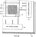
- Each sub-group of photodetectors 22 may be provided with associated array electronics dispersed in the open spaces on or in a supporting substrate 100.
- the array electronics may contain a multiplexing and clocking circuit 80, current mirror 30, a correlated double sampling circuit 40, an analog-to-digital converter 56, a sub-image pixel inverter 48, and a non-volatile memory cell 58.
- Each sub-group of photodetectors 22 is attached to a data bus 50 in response to signals from a row address decoder 60 and a column address decoder 62.
- Fig. 1B illustrates a preferred positioning of green, blue, and red photodetector elements 24 for a color sensitive array..
- the lenslet array 10 is positioned over a photosensor array 20 that may be a CCD array having a number of sub-groups of photodetectors 22 corresponding in number to at least the number of lenslets 12 forming the lenslet array 10.
- a photosensor array 20 that may be a CCD array having a number of sub-groups of photodetectors 22 corresponding in number to at least the number of lenslets 12 forming the lenslet array 10.
- a photosensor array 20 may be a CCD array having a number of sub-groups of photodetectors 22 corresponding in number to at least the number of lenslets 12 forming the lenslet array 10.
- a photosensor array 20 may be a CCD array having a number of sub-groups of photodetectors 22 corresponding in number to at least the number of lenslets 12 forming the lenslet array 10.
- a given color filter red, green, or blue
- the opaque masks 16 on the lenslet array 10 combined with a field stop aperture plate 72 limits the field of view of any particular sub-group of photodetectors 22 so that it does not overlap the field of view of it neighbors by a large amount.
- the field stop aperture plate 72 is positioned approximately 0.5mm to 3mm from the surface of the lenslet array 10.
- the field stop aperture plate 72 may be a layer of clear glass having an opaque mask pattern formed on one of it's surfaces.
- the center of the apertures in the aperture plate 72 are aligned to the center of the field of view of a corresponding lenslet.
- the spacing of the centers increases as a function of each lenslet's radial position radially from the center of the lenslet array causing the aperture plate to be slightly larger than the associated lens array.
- the combination of the opaque masks 16 with the aperture plate 72 and a given lenslet focal length determines the field of view for a sub-group of photodetectors 22.
- the lenslet array 10 can be formed of etched quartz, injection molded plastic, or an epoxy replica on a glass substrate.
- the lenslets 12 By forming the lenslets 12 with decentrations of the mechanical optical axis 14 which increase radially across the CCD array, the angle the axial ray (which is incident on a respective sub-group of photodetectors), makes with the surface normal to the photosensor array 20 will increase as a function of the radial position of a sub-group of photodetectors 22 with respect to the center of the photosensor array 20. Therefore, appropriately adjusting the decenters of each lenslet associated with a sub-group of photodetectors will allow the sub-group of photodetectors to view a different segment of a scene.
- any camera system incorporating the present invention can be extremely compact and flat.
- the camera can work in black and white or in color if color filters are used on an appropriate number of photodetector elements in the sub-group of photodetectors.
- An array of refractive aspheric lenslets can also be used to form images on the photosensor array.
- the aforementioned embodiment does not correct for the variation in focal length as a function of wavelength since the lens element is formed from a single refractive material, therefore the spot size of the incident light varies as a function of color.
- An improved optical design, including a diffractive/refractive hybrid lens is used to correct the chromatic aberration in a single material.
- n( ⁇ ) [ ⁇ c / ⁇ ](n c -1)-1
- the Sweat model is disclosed in Designing and Constructing Thick Holographic Optical Elements, " by W.C. Sweat, Applied Optics/vol. 17, No. 8, April 15, 1978, pp. 1220-1227.
- a single element lens Due to the variation of refractive index with wavelength, a single element lens has a variation of focal length with wavelength. Two materials with different dispersions can be used to form a doublet lens which has the same focal length at two wavelengths and reduced variation over the whole spectrum.
- the negative ⁇ diff of the diffractive surface allows for achromatization of single element hybrid refractive/diffractive lenses utilizing a positive focal length diffractive and refractive component. It also decreases the focal length and F/# required of the doublet component lenses, because a refractive doublet consists of a positive crown (low dispersion) lens with a shorter focal length and smaller F/# than is required for a singlet with an equivalent focal length, and a negative flint element which increases the doublet focal length to the correct value and compensates for the dispersion of the positive lens. This effect also decreases the size and weight of the positive element of a hybrid refractive/diffractive element.
- the lens array can be as a quartz master, an epoxy replica on a glass substrate, or as an injection molded part.
- diffractive/refractive hybrid achromatization enables the use of diffractive surfaces with longer focal lengths and higher F/#'s.
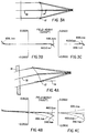
- the diffractive lenslets 12 are shown in Figs. 3A, 4A, and 5A, for the on-axis, 16 degrees, and full field of view.
- the mechanical optical axis 14 is moving radially outwards as a function of field angle while the local optical axis 18 is incident normal to the plane of the photosensor array 20.
- the opaque mask 16 acts as the aperture stop for the system as well as limiting the field of view of a given photosensor
- Figs 3B, 3C, 4B, 4C, 5B, and 5C represent the tangential and sagittal ray aberration curves for their respective lenslets.
- the solid lines represent a wavelength of 546.1 nm
- the dotted lines represent a wavelength of 656.1 nm
- the dotted and dashed lines represent a wavelength of 460.0 nm which represent light in the green, red, and blue, wavelengths.
- the focal length of the lenslet must be long enough so that when an image is formed on a given number of photodetector elements the angular resolution in the sub-group of photodetectors is comparable to the angular resolution achieved by prior art digital cameras. This establishes the lower bounds for the focal length of the lenslet in the 2-5 ⁇ m range for pixels of 3-10 microns in width.
- the following table lists the optical design parameters for three lenslets with an axial ray incident at 0, 16, and 24 degrees.
- Other lenslet surface profiles at intermediate field angles are derived by interpolating surface data between the profiles at these field angles.
- the lenslet array can operate at low F/#'s (F/2.0), it is advantageous to minimize the lenslet's diameter (increasing F/#) so as to minimize the space between lens elements and therefore the image sensor's overall dimensions. If one can achieve higher photo-signal gain with local signal processing electronics, lenslets with smaller numerical apertures can be used to generate the same level of photocurrent. This is accomplished by utilizing a multiplying current mirror.
- the lenslet diameters can be reduced by 4x to 187 ⁇ m and the length of the array will be reduced to 14.6 mm, resulting in higher photosensor yields and lower part costs.
- a digital camera can utilize this technique with little decrease in usable photosensitive surface areas since the space between each sub-group of photodetectors is not utilized for light detection. In optimizing the design of the camera, the area between sub-groups of photodetectors can be minimized to allow space only for the necessary support circuitry.
- the extra area between the sub-groups of photodetectors may be used for the incorporation of analog circuitry, sub-image pixel inverters, and from 1 to n non-volatile memory cells.
- the larger the number of memory cells the larger the number of images that can be stored.
- appropriate memory for instance, flash memory
- DRAM memory can be constructed using less surface area which allows for either a smaller distance between the sub-groups of photodetectors or more area for the storage of more image data.
- the photodetector element 24 may incorporate a CCD device and/or a photodiode.
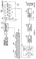
- the output of the photosensitive detector 64 is connected to a transfer gate 65 and to a reset gate 66.
- the output of the transfer gate 65 is connected to the current mirror 30A through multiplexing and clocking circuitry 80.
- the transfer gate 65 allows the charge, accumulated by the photosensitive detector 64 during the exposure period, to be transferred to the multiplying current mirror 30A at the desired time by the multiplexing and clocking circuit 80.
- the reset gate 66 allows for the emptying of the photosensitive element's accumulated charge from the previously completed exposure.
- the output from the photosensitive detector 64 is integrated for a time equivalent to the previous exposure time so as to cancel dark current and noise. This cancellation occurs within a correlated double sampling circuit (CDS) 40.
- CDS correlated double sampling circuit
- the integrated signal from the CDS circuit 40 is digitized by an analog-to-digital converter 56 and the resulting digital value is processed by the sub-image pixel inverter 48 and then stored in a non-volatile memory 58, which may be a SRAM memory.
- the digital value can be output to the main data bus 50 by accessing the unit sub-array through row and column address decoders 60 and 62, respectively.
- the image data may be stored at site and/or downloaded after each capture.
- the photosensor array 20 is then ready for exposure to a new image.
- Each photodetector element 24 in a sub-group of photodetectors 22 is connected to an individually assigned input to the multiplexing and clocking circuit 80. In operation then, the outputs from each photodetector element are serially connected (one at a time) to the current mirror 30A.
- the output of the current mirror 30A is a multiple of the current produced by the photodetector element 24.
- the current multiplying effect is traditionally accomplished either by connecting the bases or gates of the transistors 32 1 through 32 n in parallel with each other or by making the emitter (or source) areas larger by an integral multiple of the emitter area of an input side transistor 34.
- Current mirrors of this type operate on the principle that the emitter base voltage (or the gate source voltage) for all the transistors in the current mirror are the same so that each of the collector (drain) currents is the same and therefore the sum of the currents from the output side T o is a multiple of either the number of transistors in the output side or the ratio of the area.
- the output of the current mirror 30A is switched between two current amplifiers, amplifiers 42 and 44, with gains of +1 and -1, respectively.
- amplifiers 42 and 44 When the photosensitive detector 64 is receiving incident light its amplified current is switched through the +1 gain of amplifier 42 into an integrating amplifier 46 for a given amount of time and then after the shutter is closed the current is integrated through the -1 gain of amplifier 44 for an equal amount of time.
- This operation is known as dual slope, correlated double sampling, and it eliminates the effects of dark current and KTC noise. It differs from dual sample CDS in that the signal is switched through two different amplifiers depending on whether the signal represents the image data or the background data wherever dual time CDS uses the same amplification chain. Correlated double sampling also reduces Johnson noise, flicker noise, and 1/f noise.
- a similar effect can be achieved by integrating the current from an opaquely masked photodetector through the -1 gain of amplifier 44.
- Using an opaquely masked photosensor adjacent to the active photosensitive detector 64 allows the correlated double sampling technique to be implemented in parallel and decreases readout time.
- the integration of the outputs of the current amplifiers 42 and 44 occurs simultaneously, thus eliminating the need to wait for two integration periods to have output data.
- separate photosensors are used, small differences in dark current and noise can arise between them.
- ADC analog-to-digital converter
- the output of the ADC is stored in the memory cells 58 after inversion by the sub-image pixel inverter 48. It is also possible to assign a group of memory cells to each sub-group of photodetectors 22.
- the image at each sub-array of photodetectors is inverted with respect to the other sub-arrays, therefore, means for inverting the image at the sub-array are incorporated in one embodiment as a sub-image pixel inverter 48.
- This means will consist of mapping the data from one photodetector to a memory location corresponding to a photodetector at a point which is a mirror image of the object reflected about the center of the sub-array. It is also an embodiment of the invention to have the sub-array images inverted by external circuitry or by means of digital image processing.
- the invention utilizes digital image capture and processing to eliminate the need for an additional array of relay lenslets to invert the sub-images formed by each lenslet. It also eliminates the need for a third array of field lenses that would be used to maintain illumination uniformity across the lenslet's field of view.
- the stored digital pixel data is accessed by strobing the memory cells 58 via row and column address decoders, in order to send data to the data bus 50.
- the incorporation of the row and column address data lines allows for addressing of subsections of the photosensor array 20 for more rapid image readout in a specific area of interest in the image. This is useful in digital cameras which monitor a scene and are only interested in updating the section of the image associated with moving objects.
- a current mirror circuit 30B that may be substituted for the current mirror 30A, provides a second variant of the current mirror function by utilizing an output transistor T o emitter or source whose area is n times the area of the emitter or source of the input transistor T i . This forms a smaller circuit which in turn allocates more area to the sub-group of photodetector 22.
- Current mirror 30B would be substituted for the current mirror 30A at the connection point marked with a circled A.
- Fig. 8 illustrates another variant of a current mirror labeled 30C that is connectable to an associated multiplexing and clocking circuit 80 of Fig. 7 at the A labeled point marked with a circle in place of either current mirrors 30A or 30B.
- the current mirror 30C achieves current multiplication by biasing the emitter base (or gate source) voltage higher on the input side of the current mirror than on the output side. This, more specifically, is accomplished by adjusting the value of R1 and R2. Alternately, a diode junction can be substituted into the emitter or source of the input side of the current mirror 30C in order to provide a fixed voltage bias.
- data from a subsection of an array can be accessed by using only those addresses that represent the location of data of interest. In this fashion segments of a captured image may be clocked out more rapidly in order to view areas that are capturing rapid scene changes while sampling less active areas less frequently.
- the length of the addresses are increased accordingly to allow individual access to each of the multiple image data words (pixel image data).
- an object 90 is imaged onto sub-groups of photodetectors 22.
- Each lenslet 12 views a different segment of the field of view.
- the segment 1-3 of the arrow forms an inverted image 92A that impinges on its respective sub-group of photodetectors 22.
- the segment 3-5 of the arrow 90 forms an inverted image 92B that impinges on its respective sub-group of photodetectors 22.
- the segment 5-7 forming the inverted image 92C. Noted in the drawing is that the images 92A through 92C do not form, from left to right, a continuous image of the arrow 90.
- point 1 is adjacent point 5 and that point 3 is adjacent point 7 at the surfaces of the sub-group of photodetectors 22. That is, if the sub-images of the arrow 90 were simply stitched together, the overall mosaic (composite) image would be scrambled and unusable.
- the charges form the matrix of photodetector elements 24 in each sub-group 22 are first clocked out and multiplexed through their respective current multiplying circuit, correlated double sampling circuitry, and digitized by the ADC.
- the digital data from a pixel, representing an image, in each sub-group of photodetectors 22 is positionally inverted with respect to the center of each sub-group of photodetectors 22. Therefore, a sub-image pixel inverter 48 is needed to take the pixel data from a pixel located at point A and to store it in a memory cell 58 which is inverted with respect to the central pixel of the sub-group of photodetectors.
- pixel A would be stored in the memory 58 at a location corresponding to D.
- the overall mosaic composite image is then built up for use by an output device 110, such as a printer or CRT display, by reading the first row from the first sub-image and then adding the first row of the next sub-image till the first rows have all been clocked out. Next the second row from the first image is clocked out and the process continues until the mosaic image is completed with the last pixel being stored in memory location I.
- an output device 110 such as a printer or CRT display
- the overall image pixel data is generated from the array of sub-groups of photodetectors by digitally stitching the sub-images back together to form a composite image. This is accomplished by taking the row data from each sub-image in turn and adding it to the row data for the next sub-image until the end of the array is reached. Then the address for the next column of row data, at the farthest point on the array, is used to start building the next row of image data by adding the row data from the next sub-image until the end of the line of sub-arrays is reached, at which point the address pointer moves to the beginning of the next column. In some embodiments it may be useful to have some image overlap from one sub-array to the next. This would require the address decoding technique to be able to determine which location in a sub-array row is to be used as the first pixel from that row.
Landscapes
- Physics & Mathematics (AREA)
- Engineering & Computer Science (AREA)
- Multimedia (AREA)
- Signal Processing (AREA)
- General Physics & Mathematics (AREA)
- Optics & Photonics (AREA)
- Transforming Light Signals Into Electric Signals (AREA)
- Cameras In General (AREA)
- Solid State Image Pick-Up Elements (AREA)
- Color Television Image Signal Generators (AREA)
Applications Claiming Priority (2)
| Application Number | Priority Date | Filing Date | Title |
|---|---|---|---|
| US08/743,653 US6137535A (en) | 1996-11-04 | 1996-11-04 | Compact digital camera with segmented fields of view |
| US743653 | 1996-11-04 |
Publications (2)
| Publication Number | Publication Date |
|---|---|
| EP0840502A2 true EP0840502A2 (de) | 1998-05-06 |
| EP0840502A3 EP0840502A3 (de) | 2000-01-05 |
Family
ID=24989625
Family Applications (1)
| Application Number | Title | Priority Date | Filing Date |
|---|---|---|---|
| EP97203282A Withdrawn EP0840502A3 (de) | 1996-11-04 | 1997-10-23 | Kompakte Digitalkamera mit segmentierten Blickfeldern |
Country Status (3)
| Country | Link |
|---|---|
| US (1) | US6137535A (de) |
| EP (1) | EP0840502A3 (de) |
| JP (1) | JPH10145802A (de) |
Cited By (102)
| Publication number | Priority date | Publication date | Assignee | Title |
|---|---|---|---|---|
| EP0893915A3 (de) * | 1997-06-25 | 2000-01-05 | Eastman Kodak Company | Kompakter Bildsensor mit daran befestigter Bildanzeigevorrichtung |
| WO2001063914A1 (en) * | 2000-02-23 | 2001-08-30 | The Trustees Of Columbia University In The City Of New York | Method and apparatus for obtaining high dynamic range images |
| FR2819101A1 (fr) * | 2000-12-28 | 2002-07-05 | Atmel Grenoble Sa | Capteur photosensible en technologie des circuits integres |
| WO2002069618A3 (de) * | 2001-02-28 | 2002-10-24 | Infineon Technologies Ag | Digitale kamera mit einem empfindlichen sensor |
| WO2002052335A3 (en) * | 2000-12-27 | 2003-02-13 | Honeywell Int Inc | Variable focal length micro lens array field curvature corrector |
| WO2003044993A1 (de) * | 2001-11-20 | 2003-05-30 | Efkon Ag | Infrarot (ir-)-übertragungseinrichtung |
| EP1347312A1 (de) * | 2002-03-11 | 2003-09-24 | Eastman Kodak Company | An der Oberfläche geformte komplexe Polymerlinsen zur Zerstreuung von sichtbarem Licht |
| US6833873B1 (en) | 1999-06-30 | 2004-12-21 | Canon Kabushiki Kaisha | Image pickup apparatus |
| US6859229B1 (en) | 1999-06-30 | 2005-02-22 | Canon Kabushiki Kaisha | Image pickup apparatus |
| US6882368B1 (en) | 1999-06-30 | 2005-04-19 | Canon Kabushiki Kaisha | Image pickup apparatus |
| US6885404B1 (en) | 1999-06-30 | 2005-04-26 | Canon Kabushiki Kaisha | Image pickup apparatus |
| US6909554B2 (en) | 2000-12-27 | 2005-06-21 | Finisar Corporation | Wafer integration of micro-optics |
| US6980248B1 (en) | 1999-06-30 | 2005-12-27 | Canon Kabushiki Kaisha | Image pickup apparatus |
| WO2007008766A1 (en) * | 2005-07-08 | 2007-01-18 | Cdm Optics, Inc. | Ray correction apparatus and method |
| WO2007014293A1 (en) * | 2005-07-25 | 2007-02-01 | The Regents Of The University Of California | Digital imaging system and method to produce mosaic images |
| WO2007082781A1 (de) * | 2006-01-23 | 2007-07-26 | Fraunhofer-Gesellschaft zur Förderung der angewandten Forschung e.V. | Bilderfassungssystem und verfahren zur herstellung mindestens eines bilderfassungssystems |
| EP1079613A3 (de) * | 1999-08-20 | 2008-05-28 | Minolta Co., Ltd. | Bildeingabegerät |
| US7453653B2 (en) | 2004-09-14 | 2008-11-18 | Omnivision Cdm Optics, Inc. | Low height imaging system and associated methods |
| US7529383B2 (en) | 2002-10-25 | 2009-05-05 | Konica Minolta Holdings, Inc. | Image input apparatus |
| EP1695546A4 (de) * | 2003-12-18 | 2009-12-02 | Agilent Technologies Inc | Farbbildsensor mit abbildungselement-array, das bilder auf jeweiligen regionen von sensorelementen bildet |
| WO2010102985A1 (de) | 2009-03-13 | 2010-09-16 | Fraunhofer-Gesellschaft zur Förderung der angewandten Forschung e.V. | Verfahren zur herstellung einer vielzahl von mikrooptoelektronischen bauelementen und mikrooptoelektronisches bauelement |
| GB2426655B (en) * | 2005-05-05 | 2011-04-06 | Avago Technologies General Ip | Imaging device with motion sensor |
| DE102009049387A1 (de) | 2009-10-14 | 2011-04-21 | Fraunhofer-Gesellschaft zur Förderung der angewandten Forschung e.V. | Vorrichtung, Bildverarbeitungsvorrichtung und Verfahren zur optischen Abbildung |
| WO2012019875A1 (de) * | 2010-07-19 | 2012-02-16 | Fraunhofer-Gesellschaft zur Förderung der angewandten Forschung e.V. | Bildaufnahmevorrichtung und verfahren zum aufnehmen eines bildes |
| WO2011156928A3 (en) * | 2010-06-14 | 2012-02-23 | Heptagon Oy | Camera, and method of manufacturing a plurality of cameras |
| WO2013015854A1 (en) * | 2011-07-27 | 2013-01-31 | Aptina Imaging Corporation | Method and apparatus for array camera pixel readout |
| EP2637400A2 (de) * | 2012-03-09 | 2013-09-11 | Sick Ag | Bildsensor und Verfahren zur Aufnahme eines Bildes |
| EP2502115A4 (de) * | 2009-11-20 | 2013-11-06 | Pelican Imaging Corp | Aufnahme und verarbeitung von bildern mittels eines monolithischen kameraarrays mit heterogenem bildwandler |
| WO2014057104A1 (de) * | 2012-10-12 | 2014-04-17 | Fraunhofer-Gesellschaft zur Förderung der angewandten Forschung e.V. | Bildsensor und system zur optischen abbildung |
| US8792174B2 (en) | 2007-10-19 | 2014-07-29 | Fraunhofer-Gesellschaft Zur Foerderung Der Angewandten Forschung | Array of microlenses with integrated illumination |
| US8866920B2 (en) | 2008-05-20 | 2014-10-21 | Pelican Imaging Corporation | Capturing and processing of images using monolithic camera array with heterogeneous imagers |
| US8878950B2 (en) | 2010-12-14 | 2014-11-04 | Pelican Imaging Corporation | Systems and methods for synthesizing high resolution images using super-resolution processes |
| US8885059B1 (en) | 2008-05-20 | 2014-11-11 | Pelican Imaging Corporation | Systems and methods for measuring depth using images captured by camera arrays |
| US8928793B2 (en) | 2010-05-12 | 2015-01-06 | Pelican Imaging Corporation | Imager array interfaces |
| US9025895B2 (en) | 2011-09-28 | 2015-05-05 | Pelican Imaging Corporation | Systems and methods for decoding refocusable light field image files |
| FR3013135A1 (fr) * | 2013-11-14 | 2015-05-15 | Imao | Appareil photographique a tres haute resolution et a tres grande taille d'image |
| US9100586B2 (en) | 2013-03-14 | 2015-08-04 | Pelican Imaging Corporation | Systems and methods for photometric normalization in array cameras |
| US9100635B2 (en) | 2012-06-28 | 2015-08-04 | Pelican Imaging Corporation | Systems and methods for detecting defective camera arrays and optic arrays |
| US9106784B2 (en) | 2013-03-13 | 2015-08-11 | Pelican Imaging Corporation | Systems and methods for controlling aliasing in images captured by an array camera for use in super-resolution processing |
| US9123117B2 (en) | 2012-08-21 | 2015-09-01 | Pelican Imaging Corporation | Systems and methods for generating depth maps and corresponding confidence maps indicating depth estimation reliability |
| US9124864B2 (en) | 2013-03-10 | 2015-09-01 | Pelican Imaging Corporation | System and methods for calibration of an array camera |
| US9128228B2 (en) | 2011-06-28 | 2015-09-08 | Pelican Imaging Corporation | Optical arrangements for use with an array camera |
| US9143711B2 (en) | 2012-11-13 | 2015-09-22 | Pelican Imaging Corporation | Systems and methods for array camera focal plane control |
| US9185276B2 (en) | 2013-11-07 | 2015-11-10 | Pelican Imaging Corporation | Methods of manufacturing array camera modules incorporating independently aligned lens stacks |
| US9197821B2 (en) | 2011-05-11 | 2015-11-24 | Pelican Imaging Corporation | Systems and methods for transmitting and receiving array camera image data |
| US9210392B2 (en) | 2012-05-01 | 2015-12-08 | Pelican Imaging Coporation | Camera modules patterned with pi filter groups |
| US9214013B2 (en) | 2012-09-14 | 2015-12-15 | Pelican Imaging Corporation | Systems and methods for correcting user identified artifacts in light field images |
| US9247117B2 (en) | 2014-04-07 | 2016-01-26 | Pelican Imaging Corporation | Systems and methods for correcting for warpage of a sensor array in an array camera module by introducing warpage into a focal plane of a lens stack array |
| US9253380B2 (en) | 2013-02-24 | 2016-02-02 | Pelican Imaging Corporation | Thin form factor computational array cameras and modular array cameras |
| WO2016096165A1 (en) * | 2014-12-19 | 2016-06-23 | Sony Corporation | Noise level based exposure time control for sequential subimages |
| US9412206B2 (en) | 2012-02-21 | 2016-08-09 | Pelican Imaging Corporation | Systems and methods for the manipulation of captured light field image data |
| US9426361B2 (en) | 2013-11-26 | 2016-08-23 | Pelican Imaging Corporation | Array camera configurations incorporating multiple constituent array cameras |
| US9438888B2 (en) | 2013-03-15 | 2016-09-06 | Pelican Imaging Corporation | Systems and methods for stereo imaging with camera arrays |
| CN105934944A (zh) * | 2013-11-26 | 2016-09-07 | 株式会社尼康 | 电子设备、摄像装置及摄像元件 |
| US9445003B1 (en) | 2013-03-15 | 2016-09-13 | Pelican Imaging Corporation | Systems and methods for synthesizing high resolution images using image deconvolution based on motion and depth information |
| US9462164B2 (en) | 2013-02-21 | 2016-10-04 | Pelican Imaging Corporation | Systems and methods for generating compressed light field representation data using captured light fields, array geometry, and parallax information |
| US9497429B2 (en) | 2013-03-15 | 2016-11-15 | Pelican Imaging Corporation | Extended color processing on pelican array cameras |
| US9497370B2 (en) | 2013-03-15 | 2016-11-15 | Pelican Imaging Corporation | Array camera architecture implementing quantum dot color filters |
| US9516222B2 (en) | 2011-06-28 | 2016-12-06 | Kip Peli P1 Lp | Array cameras incorporating monolithic array camera modules with high MTF lens stacks for capture of images used in super-resolution processing |
| US9519972B2 (en) | 2013-03-13 | 2016-12-13 | Kip Peli P1 Lp | Systems and methods for synthesizing images from image data captured by an array camera using restricted depth of field depth maps in which depth estimation precision varies |
| US9521319B2 (en) | 2014-06-18 | 2016-12-13 | Pelican Imaging Corporation | Array cameras and array camera modules including spectral filters disposed outside of a constituent image sensor |
| US9521416B1 (en) | 2013-03-11 | 2016-12-13 | Kip Peli P1 Lp | Systems and methods for image data compression |
| DE102012202386B4 (de) * | 2011-02-17 | 2017-02-09 | Canon Kabushiki Kaisha | Bildaufnahmevorrichtung, bildsignalverarbeitungsvorrichtung und steuerverfahren von bildaufnahmevorrichtung |
| US9578259B2 (en) | 2013-03-14 | 2017-02-21 | Fotonation Cayman Limited | Systems and methods for reducing motion blur in images or video in ultra low light with array cameras |
| US9633442B2 (en) | 2013-03-15 | 2017-04-25 | Fotonation Cayman Limited | Array cameras including an array camera module augmented with a separate camera |
| US9638883B1 (en) | 2013-03-04 | 2017-05-02 | Fotonation Cayman Limited | Passive alignment of array camera modules constructed from lens stack arrays and sensors based upon alignment information obtained during manufacture of array camera modules using an active alignment process |
| US9741118B2 (en) | 2013-03-13 | 2017-08-22 | Fotonation Cayman Limited | System and methods for calibration of an array camera |
| US9766380B2 (en) | 2012-06-30 | 2017-09-19 | Fotonation Cayman Limited | Systems and methods for manufacturing camera modules using active alignment of lens stack arrays and sensors |
| US9774789B2 (en) | 2013-03-08 | 2017-09-26 | Fotonation Cayman Limited | Systems and methods for high dynamic range imaging using array cameras |
| US9794476B2 (en) | 2011-09-19 | 2017-10-17 | Fotonation Cayman Limited | Systems and methods for controlling aliasing in images captured by an array camera for use in super resolution processing using pixel apertures |
| US9813616B2 (en) | 2012-08-23 | 2017-11-07 | Fotonation Cayman Limited | Feature based high resolution motion estimation from low resolution images captured using an array source |
| US9888194B2 (en) | 2013-03-13 | 2018-02-06 | Fotonation Cayman Limited | Array camera architecture implementing quantum film image sensors |
| US9898856B2 (en) | 2013-09-27 | 2018-02-20 | Fotonation Cayman Limited | Systems and methods for depth-assisted perspective distortion correction |
| US9942474B2 (en) | 2015-04-17 | 2018-04-10 | Fotonation Cayman Limited | Systems and methods for performing high speed video capture and depth estimation using array cameras |
| WO2018019406A3 (de) * | 2016-07-25 | 2018-04-26 | Universität Duisburg-Essen | System zur gleichzeitigen videografischen oder fotografischen erfassung von mehreren bildern |
| US10089740B2 (en) | 2014-03-07 | 2018-10-02 | Fotonation Limited | System and methods for depth regularization and semiautomatic interactive matting using RGB-D images |
| US10122993B2 (en) | 2013-03-15 | 2018-11-06 | Fotonation Limited | Autofocus system for a conventional camera that uses depth information from an array camera |
| US10119808B2 (en) | 2013-11-18 | 2018-11-06 | Fotonation Limited | Systems and methods for estimating depth from projected texture using camera arrays |
| US10250871B2 (en) | 2014-09-29 | 2019-04-02 | Fotonation Limited | Systems and methods for dynamic calibration of array cameras |
| WO2019101750A3 (en) * | 2017-11-21 | 2019-08-01 | CSEM Centre Suisse d'Electronique et de Microtechnique SA - Recherche et Développement | Spectrometer |
| US10390005B2 (en) | 2012-09-28 | 2019-08-20 | Fotonation Limited | Generating images from light fields utilizing virtual viewpoints |
| US10482618B2 (en) | 2017-08-21 | 2019-11-19 | Fotonation Limited | Systems and methods for hybrid depth regularization |
| US10916575B2 (en) | 2018-04-04 | 2021-02-09 | Samsung Electronics Co., Ltd. | Image sensor and method of manufacturing image sensor |
| KR20210088375A (ko) | 2020-01-06 | 2021-07-14 | 엘아이지넥스원 주식회사 | 마이크로 렌즈 어레이 및 이를 포함하는 이미지 센서모듈과 그 제조방법 |
| US11270110B2 (en) | 2019-09-17 | 2022-03-08 | Boston Polarimetrics, Inc. | Systems and methods for surface modeling using polarization cues |
| US11290658B1 (en) | 2021-04-15 | 2022-03-29 | Boston Polarimetrics, Inc. | Systems and methods for camera exposure control |
| CN114323310A (zh) * | 2021-12-28 | 2022-04-12 | 中国科学院光电技术研究所 | 一种高分辨率哈特曼波前传感器 |
| US11302012B2 (en) | 2019-11-30 | 2022-04-12 | Boston Polarimetrics, Inc. | Systems and methods for transparent object segmentation using polarization cues |
| US11525906B2 (en) | 2019-10-07 | 2022-12-13 | Intrinsic Innovation Llc | Systems and methods for augmentation of sensor systems and imaging systems with polarization |
| US11580667B2 (en) | 2020-01-29 | 2023-02-14 | Intrinsic Innovation Llc | Systems and methods for characterizing object pose detection and measurement systems |
| US11689813B2 (en) | 2021-07-01 | 2023-06-27 | Intrinsic Innovation Llc | Systems and methods for high dynamic range imaging using crossed polarizers |
| US11792538B2 (en) | 2008-05-20 | 2023-10-17 | Adeia Imaging Llc | Capturing and processing of images including occlusions focused on an image sensor by a lens stack array |
| US11797863B2 (en) | 2020-01-30 | 2023-10-24 | Intrinsic Innovation Llc | Systems and methods for synthesizing data for training statistical models on different imaging modalities including polarized images |
| US11954886B2 (en) | 2021-04-15 | 2024-04-09 | Intrinsic Innovation Llc | Systems and methods for six-degree of freedom pose estimation of deformable objects |
| US11953700B2 (en) | 2020-05-27 | 2024-04-09 | Intrinsic Innovation Llc | Multi-aperture polarization optical systems using beam splitters |
| US12020455B2 (en) | 2021-03-10 | 2024-06-25 | Intrinsic Innovation Llc | Systems and methods for high dynamic range image reconstruction |
| US12069227B2 (en) | 2021-03-10 | 2024-08-20 | Intrinsic Innovation Llc | Multi-modal and multi-spectral stereo camera arrays |
| US12067746B2 (en) | 2021-05-07 | 2024-08-20 | Intrinsic Innovation Llc | Systems and methods for using computer vision to pick up small objects |
| US12172310B2 (en) | 2021-06-29 | 2024-12-24 | Intrinsic Innovation Llc | Systems and methods for picking objects using 3-D geometry and segmentation |
| US12175741B2 (en) | 2021-06-22 | 2024-12-24 | Intrinsic Innovation Llc | Systems and methods for a vision guided end effector |
| US12293535B2 (en) | 2021-08-03 | 2025-05-06 | Intrinsic Innovation Llc | Systems and methods for training pose estimators in computer vision |
| US12340538B2 (en) | 2021-06-25 | 2025-06-24 | Intrinsic Innovation Llc | Systems and methods for generating and using visual datasets for training computer vision models |
Families Citing this family (132)
| Publication number | Priority date | Publication date | Assignee | Title |
|---|---|---|---|---|
| NO305728B1 (no) * | 1997-11-14 | 1999-07-12 | Reidar E Tangen | Optoelektronisk kamera og fremgangsmÕte ved bildeformatering i samme |
| US6552745B1 (en) * | 1998-04-08 | 2003-04-22 | Agilent Technologies, Inc. | CMOS active pixel with memory for imaging sensors |
| US6657663B2 (en) * | 1998-05-06 | 2003-12-02 | Intel Corporation | Pre-subtracting architecture for enabling multiple spectrum image sensing |
| US7129978B1 (en) | 1998-07-13 | 2006-10-31 | Zoran Corporation | Method and architecture for an improved CMOS color image sensor |
| JP3927702B2 (ja) * | 1998-09-24 | 2007-06-13 | キヤノン株式会社 | 画像処理装置、自動焦点検出装置、補正装置、補正方法及び記憶媒体 |
| US6657749B1 (en) * | 1998-10-01 | 2003-12-02 | Honeywell International Inc. | Scanner using lens array producing inverted images |
| JP3531908B2 (ja) * | 1999-02-17 | 2004-05-31 | キヤノン株式会社 | 撮像装置、放射線検出装置および画像処理システム |
| US7176446B1 (en) * | 1999-09-15 | 2007-02-13 | Zoran Corporation | Method and apparatus for distributing light onto electronic image sensors |
| US7133074B1 (en) * | 1999-09-28 | 2006-11-07 | Zoran Corporation | Image sensor circuits including sampling circuits used therein for performing correlated double sampling |
| US7123292B1 (en) * | 1999-09-29 | 2006-10-17 | Xerox Corporation | Mosaicing images with an offset lens |
| US6605488B1 (en) * | 1999-10-12 | 2003-08-12 | Micron Technology, Inc. | Layout technique for semiconductor processing using stitching |
| US6995800B2 (en) * | 2000-01-27 | 2006-02-07 | Canon Kabushiki Kaisha | Image pickup apparatus utilizing a plurality of converging lenses |
| TW475334B (en) * | 2000-07-14 | 2002-02-01 | Light Opto Electronics Co Ltd | High light-sensing efficiency image sensor apparatus and method of making the same |
| WO2002011406A2 (en) * | 2000-07-31 | 2002-02-07 | Koninklijke Philips Electronics N.V. | Image-sensing display device |
| US6750437B2 (en) * | 2000-08-28 | 2004-06-15 | Canon Kabushiki Kaisha | Image pickup apparatus that suitably adjusts a focus |
| US6952228B2 (en) * | 2000-10-13 | 2005-10-04 | Canon Kabushiki Kaisha | Image pickup apparatus |
| US7139028B2 (en) * | 2000-10-17 | 2006-11-21 | Canon Kabushiki Kaisha | Image pickup apparatus |
| US6950129B1 (en) * | 2000-11-22 | 2005-09-27 | Hewlett-Packard Development Company, L.P. | One-time-use digital camera |
| US7034866B1 (en) * | 2000-11-22 | 2006-04-25 | Koninklijke Philips Electronics N.V. | Combined display-camera for an image processing system |
| JP4500434B2 (ja) * | 2000-11-28 | 2010-07-14 | キヤノン株式会社 | 撮像装置及び撮像システム、並びに撮像方法 |
| JP2002171537A (ja) * | 2000-11-30 | 2002-06-14 | Canon Inc | 複眼撮像系、撮像装置および電子機器 |
| GB0029947D0 (en) * | 2000-12-08 | 2001-01-24 | Sgs Thomson Microelectronics | Solid state image sensors and microlens arrays |
| JP2002252338A (ja) * | 2000-12-18 | 2002-09-06 | Canon Inc | 撮像装置及び撮像システム |
| US6791073B1 (en) * | 2000-12-21 | 2004-09-14 | Terabeam Corporation | Optical receiver having baffle including a plurality of apertures |
| JP2002232789A (ja) * | 2001-02-05 | 2002-08-16 | Univ Tokyo | 撮像方法及び撮像装置 |
| EP1384046B1 (de) * | 2001-05-04 | 2018-10-03 | Vexcel Imaging GmbH | Digitalkamera und verfahren zum erzeugen von sich überdeckenden bildern |
| JP3518529B2 (ja) * | 2001-08-17 | 2004-04-12 | ソニー株式会社 | 固体撮像装置 |
| US6894719B2 (en) * | 2001-08-23 | 2005-05-17 | Eastman Kodak Company | Method and apparatus for creating a preselected lenticular image |
| JP4920839B2 (ja) * | 2001-09-18 | 2012-04-18 | キヤノン株式会社 | 撮像装置 |
| JP2003143459A (ja) * | 2001-11-02 | 2003-05-16 | Canon Inc | 複眼撮像系およびこれを備えた装置 |
| JP3742775B2 (ja) * | 2002-02-21 | 2006-02-08 | 富士フイルムマイクロデバイス株式会社 | 固体撮像素子 |
| JP2004007413A (ja) * | 2002-03-28 | 2004-01-08 | Hiroyuki Ogino | 画像入力装置及びその方法 |
| JP2004032172A (ja) * | 2002-06-24 | 2004-01-29 | Canon Inc | 複眼撮像装置およびこれを備えた機器 |
| US7423679B2 (en) * | 2002-12-20 | 2008-09-09 | Eastman Kodak Company | Imaging system having extended useful latitude |
| KR20040068438A (ko) * | 2003-01-25 | 2004-07-31 | 삼성전자주식회사 | 보행식 로봇 및 그 위치이동방법 |
| JP3709873B2 (ja) * | 2003-02-19 | 2005-10-26 | ソニー株式会社 | 固体撮像装置及び撮像カメラ |
| US6801719B1 (en) * | 2003-03-14 | 2004-10-05 | Eastman Kodak Company | Camera using beam splitter with micro-lens image amplification |
| US7196301B2 (en) * | 2003-07-18 | 2007-03-27 | Honeywell International, Inc. | System for detecting incoming light from a remote laser source |
| US20080121826A1 (en) * | 2003-07-18 | 2008-05-29 | Honeywell International Inc. | Laser source detection system and method |
| JP2005065064A (ja) * | 2003-08-19 | 2005-03-10 | Olympus Corp | 電子撮像装置 |
| US7310477B2 (en) * | 2003-08-26 | 2007-12-18 | Eastman Kodak Company | Photographic film cartridge or cassette systems with microlens |
| US7405761B2 (en) | 2003-10-01 | 2008-07-29 | Tessera North America, Inc. | Thin camera having sub-pixel resolution |
| US20050128509A1 (en) * | 2003-12-11 | 2005-06-16 | Timo Tokkonen | Image creating method and imaging device |
| JP4411059B2 (ja) * | 2003-12-12 | 2010-02-10 | キヤノン株式会社 | カメラ付きディスプレイ装置、通信装置および通信システム |
| JP2005197379A (ja) * | 2004-01-06 | 2005-07-21 | Sony Corp | 固体撮像装置および信号処理回路 |
| DE102004003013B3 (de) * | 2004-01-20 | 2005-06-02 | Fraunhofer-Gesellschaft zur Förderung der angewandten Forschung e.V. | Bilderfassungssystem und dessen Verwendung |
| EP2315448B1 (de) * | 2004-01-26 | 2018-03-07 | DigitalOptics Corporation | Dünne kamera mit subpixel-auflösung |
| US7773143B2 (en) * | 2004-04-08 | 2010-08-10 | Tessera North America, Inc. | Thin color camera having sub-pixel resolution |
| US8724006B2 (en) * | 2004-01-26 | 2014-05-13 | Flir Systems, Inc. | Focal plane coding for digital imaging |
| TWI275830B (en) * | 2004-02-25 | 2007-03-11 | Synge Technology Corpation | Lens for chromatic aberration compensating |
| US8953087B2 (en) * | 2004-04-08 | 2015-02-10 | Flir Systems Trading Belgium Bvba | Camera system and associated methods |
| US8049806B2 (en) * | 2004-09-27 | 2011-11-01 | Digitaloptics Corporation East | Thin camera and associated methods |
| US7564019B2 (en) * | 2005-08-25 | 2009-07-21 | Richard Ian Olsen | Large dynamic range cameras |
| US7795577B2 (en) * | 2004-08-25 | 2010-09-14 | Richard Ian Olsen | Lens frame and optical focus assembly for imager module |
| EP1812968B1 (de) | 2004-08-25 | 2019-01-16 | Callahan Cellular L.L.C. | Vorrichtung für mehrere kameraeinrichtungen und verfahren zu ihrem betrieb |
| US7916180B2 (en) * | 2004-08-25 | 2011-03-29 | Protarius Filo Ag, L.L.C. | Simultaneous multiple field of view digital cameras |
| US8124929B2 (en) | 2004-08-25 | 2012-02-28 | Protarius Filo Ag, L.L.C. | Imager module optical focus and assembly method |
| US20060044451A1 (en) * | 2004-08-30 | 2006-03-02 | Eastman Kodak Company | Wide angle lenslet camera |
| US20060055811A1 (en) * | 2004-09-14 | 2006-03-16 | Frtiz Bernard S | Imaging system having modules with adaptive optical elements |
| US20060215054A1 (en) * | 2005-03-23 | 2006-09-28 | Eastman Kodak Company | Wide angle camera with prism array |
| CN101147392B (zh) * | 2005-03-24 | 2012-05-09 | 松下电器产业株式会社 | 成像装置及其中使用的透镜阵列 |
| FR2884338B1 (fr) * | 2005-04-11 | 2007-10-19 | Valeo Vision Sa | Procede, dispositif et camera pour la detection d'objets a partir d'images numeriques |
| US20070102622A1 (en) * | 2005-07-01 | 2007-05-10 | Olsen Richard I | Apparatus for multiple camera devices and method of operating same |
| US20070258006A1 (en) * | 2005-08-25 | 2007-11-08 | Olsen Richard I | Solid state camera optics frame and assembly |
| US7566855B2 (en) * | 2005-08-25 | 2009-07-28 | Richard Ian Olsen | Digital camera with integrated infrared (IR) response |
| US7964835B2 (en) | 2005-08-25 | 2011-06-21 | Protarius Filo Ag, L.L.C. | Digital cameras with direct luminance and chrominance detection |
| JP4306676B2 (ja) * | 2005-12-19 | 2009-08-05 | 船井電機株式会社 | 撮像装置 |
| US7620309B2 (en) * | 2006-04-04 | 2009-11-17 | Adobe Systems, Incorporated | Plenoptic camera |
| US20070263114A1 (en) * | 2006-05-01 | 2007-11-15 | Microalign Technologies, Inc. | Ultra-thin digital imaging device of high resolution for mobile electronic devices and method of imaging |
| WO2007132787A1 (ja) * | 2006-05-15 | 2007-11-22 | Panasonic Corporation | 回折撮像レンズと回折撮像レンズ光学系及びこれを用いた撮像装置 |
| US7714998B2 (en) * | 2006-11-28 | 2010-05-11 | Applied Materials South East Asia Pte. Ltd. | Image splitting in optical inspection systems |
| US7719674B2 (en) * | 2006-11-28 | 2010-05-18 | Applied Materials South East Asia Pte. Ltd. | Image splitting in optical inspection systems |
| US7604360B2 (en) * | 2006-12-29 | 2009-10-20 | Avago Technologies Ecbu Ip (Singapore) Pte. Ltd. | Integrated sensor for correlated color temperature and illuminance sensing |
| JP4653123B2 (ja) * | 2007-01-09 | 2011-03-16 | 富士フイルム株式会社 | 画像取得装置および画像取得方法 |
| JP4985061B2 (ja) * | 2007-04-06 | 2012-07-25 | 株式会社ニコン | 分光装置および撮像装置 |
| US8290358B1 (en) * | 2007-06-25 | 2012-10-16 | Adobe Systems Incorporated | Methods and apparatus for light-field imaging |
| US8559756B2 (en) | 2007-08-06 | 2013-10-15 | Adobe Systems Incorporated | Radiance processing by demultiplexing in the frequency domain |
| US7962033B2 (en) * | 2008-01-23 | 2011-06-14 | Adobe Systems Incorporated | Methods and apparatus for full-resolution light-field capture and rendering |
| US8189065B2 (en) | 2008-01-23 | 2012-05-29 | Adobe Systems Incorporated | Methods and apparatus for full-resolution light-field capture and rendering |
| JP4941332B2 (ja) * | 2008-01-28 | 2012-05-30 | ソニー株式会社 | 撮像装置 |
| US8155456B2 (en) * | 2008-04-29 | 2012-04-10 | Adobe Systems Incorporated | Method and apparatus for block-based compression of light-field images |
| US8244058B1 (en) | 2008-05-30 | 2012-08-14 | Adobe Systems Incorporated | Method and apparatus for managing artifacts in frequency domain processing of light-field images |
| EP2133726B1 (de) | 2008-06-10 | 2011-06-01 | Thomson Licensing | Mehrbildaufnahmesystem mit verbesserter Tiefenbildauflösung |
| JP4582205B2 (ja) * | 2008-06-12 | 2010-11-17 | トヨタ自動車株式会社 | 電動車両 |
| US8436909B2 (en) | 2008-10-21 | 2013-05-07 | Stmicroelectronics S.R.L. | Compound camera sensor and related method of processing digital images |
| FR2940720B1 (fr) * | 2008-12-31 | 2011-03-18 | St Microelectronics Sa | Dispositif de saisie d'images comprenant des moyens de correction de mise au point |
| US9635253B2 (en) | 2009-01-05 | 2017-04-25 | Duke University | Multiscale telescopic imaging system |
| US9432591B2 (en) | 2009-01-05 | 2016-08-30 | Duke University | Multiscale optical system having dynamic camera settings |
| US8259212B2 (en) * | 2009-01-05 | 2012-09-04 | Applied Quantum Technologies, Inc. | Multiscale optical system |
| US9395617B2 (en) * | 2009-01-05 | 2016-07-19 | Applied Quantum Technologies, Inc. | Panoramic multi-scale imager and method therefor |
| US9494771B2 (en) | 2009-01-05 | 2016-11-15 | Duke University | Quasi-monocentric-lens-based multi-scale optical system |
| US10725280B2 (en) | 2009-01-05 | 2020-07-28 | Duke University | Multiscale telescopic imaging system |
| US8830377B2 (en) * | 2010-01-04 | 2014-09-09 | Duke University | Monocentric lens-based multi-scale optical systems and methods of use |
| US8189089B1 (en) | 2009-01-20 | 2012-05-29 | Adobe Systems Incorporated | Methods and apparatus for reducing plenoptic camera artifacts |
| US8315476B1 (en) | 2009-01-20 | 2012-11-20 | Adobe Systems Incorporated | Super-resolution with the focused plenoptic camera |
| US8345144B1 (en) | 2009-07-15 | 2013-01-01 | Adobe Systems Incorporated | Methods and apparatus for rich image capture with focused plenoptic cameras |
| US8228417B1 (en) | 2009-07-15 | 2012-07-24 | Adobe Systems Incorporated | Focused plenoptic camera employing different apertures or filtering at different microlenses |
| US20110026141A1 (en) * | 2009-07-29 | 2011-02-03 | Geoffrey Louis Barrows | Low Profile Camera and Vision Sensor |
| DE102009056178A1 (de) * | 2009-11-27 | 2011-06-01 | Carl Zeiss Ag | Bildaufnehmer, Bilderzeugungseinrichtung sowie Spektroskop für die ortsaufgelöste Spektroskopie |
| US8400555B1 (en) | 2009-12-01 | 2013-03-19 | Adobe Systems Incorporated | Focused plenoptic camera employing microlenses with different focal lengths |
| US20110205384A1 (en) * | 2010-02-24 | 2011-08-25 | Panavision Imaging, Llc | Variable active image area image sensor |
| US8817015B2 (en) | 2010-03-03 | 2014-08-26 | Adobe Systems Incorporated | Methods, apparatus, and computer-readable storage media for depth-based rendering of focused plenoptic camera data |
| US8358366B1 (en) | 2010-05-28 | 2013-01-22 | Adobe Systems Incorporate | Methods and apparatus for high-speed digital imaging |
| US8803918B2 (en) | 2010-08-27 | 2014-08-12 | Adobe Systems Incorporated | Methods and apparatus for calibrating focused plenoptic camera data |
| US8665341B2 (en) | 2010-08-27 | 2014-03-04 | Adobe Systems Incorporated | Methods and apparatus for rendering output images with simulated artistic effects from focused plenoptic camera data |
| US8724000B2 (en) | 2010-08-27 | 2014-05-13 | Adobe Systems Incorporated | Methods and apparatus for super-resolution in integral photography |
| US8749694B2 (en) | 2010-08-27 | 2014-06-10 | Adobe Systems Incorporated | Methods and apparatus for rendering focused plenoptic camera data using super-resolved demosaicing |
| US20120188391A1 (en) * | 2011-01-25 | 2012-07-26 | Scott Smith | Array camera having lenses with independent fields of view |
| GB2488519A (en) * | 2011-02-16 | 2012-09-05 | St Microelectronics Res & Dev | Multi-channel image sensor incorporating lenslet array and overlapping fields of view. |
| US9197798B2 (en) | 2011-03-25 | 2015-11-24 | Adobe Systems Incorporated | Thin plenoptic cameras using microspheres |
| US20120274811A1 (en) * | 2011-04-28 | 2012-11-01 | Dmitry Bakin | Imaging devices having arrays of image sensors and precision offset lenses |
| CN103620782B (zh) * | 2011-07-08 | 2016-04-13 | 松下知识产权经营株式会社 | 固体摄像元件以及摄像装置 |
| JP5705140B2 (ja) * | 2011-09-27 | 2015-04-22 | 株式会社東芝 | 固体撮像装置及び固体撮像装置の製造方法 |
| US8928969B2 (en) | 2011-12-06 | 2015-01-06 | Ostendo Technologies, Inc. | Spatio-optical directional light modulator |
| US8854724B2 (en) | 2012-03-27 | 2014-10-07 | Ostendo Technologies, Inc. | Spatio-temporal directional light modulator |
| US9179126B2 (en) | 2012-06-01 | 2015-11-03 | Ostendo Technologies, Inc. | Spatio-temporal light field cameras |
| EP2677734A3 (de) * | 2012-06-18 | 2016-01-13 | Sony Mobile Communications AB | Arraykameraabbildungssystem und Verfahren |
| WO2014137922A1 (en) | 2013-03-05 | 2014-09-12 | Rambus Inc. | Phase gratings with odd symmetry for high-resoultion lensless optical sensing |
| WO2014196322A1 (ja) * | 2013-06-05 | 2014-12-11 | コニカミノルタ株式会社 | 複眼撮像光学系及び複眼撮像装置 |
| US9515113B2 (en) * | 2013-08-27 | 2016-12-06 | Rambus Inc. | Optical sensing of nearby scenes with tessellated phase anti-symmetric gratings |
| US9880391B2 (en) * | 2013-10-01 | 2018-01-30 | Heptagon Micro Optics Pte. Ltd. | Lens array modules and wafer-level techniques for fabricating the same |
| DE102013226196A1 (de) * | 2013-12-17 | 2015-06-18 | Volkswagen Aktiengesellschaft | Optisches Sensorsystem |
| WO2016033590A1 (en) | 2014-08-31 | 2016-03-03 | Berestka John | Systems and methods for analyzing the eye |
| US10935775B2 (en) * | 2017-05-18 | 2021-03-02 | Phoneoptika Ltd | Method and apparatus that enhance the viewing experience of digital displays for long sighted users |
| US10539718B2 (en) * | 2017-08-17 | 2020-01-21 | Honeywell International Inc. | Fresnel lens array with improved off-axis optical efficiency |
| KR102614907B1 (ko) * | 2018-04-04 | 2023-12-19 | 삼성전자주식회사 | 이미지 센서 및 이미지 센서 제조 방법 |
| US11333748B2 (en) | 2018-09-17 | 2022-05-17 | Waymo Llc | Array of light detectors with corresponding array of optical elements |
| US11328150B2 (en) * | 2020-04-30 | 2022-05-10 | Omnivision Technologies, Inc. | Lens-array imager |
| US11902638B1 (en) | 2020-12-30 | 2024-02-13 | Ball Aerospace & Technologies Corp. | Gapless detector mosaic imaging systems and methods |
| US12106599B2 (en) | 2022-06-13 | 2024-10-01 | Omnivision Technologies, Inc. | Thin, multi-lens, optical fingerprint sensor adapted to image through cell phone displays and with multiple photodiode groups each having separate fields of view for each microlens |
| GB2635586A (en) | 2023-11-07 | 2025-05-21 | Lightfield Medical Inc | Systems and methods for analyzing the eye |
| WO2025218987A1 (en) * | 2024-04-17 | 2025-10-23 | Ams-Osram Ag | Optical detector, picture-recording device and manufacturing method |
Family Cites Families (26)
| Publication number | Priority date | Publication date | Assignee | Title |
|---|---|---|---|---|
| US3910683A (en) * | 1970-07-28 | 1975-10-07 | Minolta Camera Kk | Optical low-pass filter |
| JPS54154728A (en) * | 1978-05-25 | 1979-12-06 | Boehringer Mannheim Gmbh | Manufacture of alphaa*44*44chlorobenzoylaminoo ethyl**phenoxyyisoethylacetic acid |
| DE2823164A1 (de) * | 1978-05-26 | 1979-11-29 | Bayer Ag | Verfahren zur herstellung von hexahydrophthalsaeureanhydrid |
| US4318123A (en) * | 1980-06-05 | 1982-03-02 | Rca Corporation | Solid-state, color-encoding television camera |
| US4323925A (en) * | 1980-07-07 | 1982-04-06 | Avco Everett Research Laboratory, Inc. | Method and apparatus for arraying image sensor modules |
| JPS57184376A (en) * | 1981-05-09 | 1982-11-13 | Sony Corp | Signal output circuit of image pickup device |
| US4377753A (en) * | 1981-06-01 | 1983-03-22 | Eastman Kodak Company | High resolution optical-addressing device and electronic scanner and/or printer apparatus employing such device |
| JPS59193699A (ja) * | 1983-04-18 | 1984-11-02 | Niles Parts Co Ltd | 平面駆動型スピ−カ |
| US4708436A (en) * | 1985-07-12 | 1987-11-24 | Rca Corporation | Optical imager with diffractive lenticular array |
| US4689291A (en) * | 1985-08-30 | 1987-08-25 | Xerox Corporation | Pedestal-type microlens fabrication process |
| JPS62144459A (ja) * | 1985-12-19 | 1987-06-27 | Ricoh Co Ltd | 完全密着型センサ− |
| US5004901A (en) * | 1987-06-04 | 1991-04-02 | Mitsubishi Denki Kabushiki Kaisha | Current mirror amplifier for use in an optical data medium driving apparatus and servo-circuit |
| US5187358A (en) * | 1989-02-15 | 1993-02-16 | Canon Kabushiki Kaisha | Image reading device having a telecentric optical system and a blazed diffraction grating |
| US4994664A (en) * | 1989-03-27 | 1991-02-19 | Massachusetts Institute Of Technology | Optically coupled focal plane arrays using lenslets and multiplexers |
| US5151790A (en) * | 1990-07-23 | 1992-09-29 | Fuji Photo Film Co., Ltd. | Image pickup device for stabilizing optical aberrations |
| US5076687A (en) * | 1990-08-28 | 1991-12-31 | Massachusetts Institute Of Technology | Optical ranging apparatus |
| GB2251700B (en) * | 1990-11-30 | 1994-08-24 | Combined Optical Ind Ltd | Multiple array lens |
| US5233174A (en) * | 1992-03-11 | 1993-08-03 | Hughes Danbury Optical Systems, Inc. | Wavefront sensor having a lenslet array as a null corrector |
| US5497269A (en) * | 1992-06-25 | 1996-03-05 | Lockheed Missiles And Space Company, Inc. | Dispersive microlens |
| US5760834A (en) * | 1992-09-30 | 1998-06-02 | Lsi Logic | Electronic camera with binary lens element array |
| US5340978A (en) * | 1992-09-30 | 1994-08-23 | Lsi Logic Corporation | Image-sensing display panels with LCD display panel and photosensitive element array |
| US5471515A (en) * | 1994-01-28 | 1995-11-28 | California Institute Of Technology | Active pixel sensor with intra-pixel charge transfer |
| US5461425A (en) * | 1994-02-15 | 1995-10-24 | Stanford University | CMOS image sensor with pixel level A/D conversion |
| JPH08107194A (ja) * | 1994-10-03 | 1996-04-23 | Fuji Photo Optical Co Ltd | 固体撮像装置 |
| US6141048A (en) * | 1996-08-19 | 2000-10-31 | Eastman Kodak Company | Compact image capture device |
| EP0833502A3 (de) * | 1996-09-26 | 2000-01-05 | Eastman Kodak Company | Kompakte Bildaufnahmevorrichtung mit örtlichem Bildspeicher |
-
1996
- 1996-11-04 US US08/743,653 patent/US6137535A/en not_active Expired - Lifetime
-
1997
- 1997-10-23 EP EP97203282A patent/EP0840502A3/de not_active Withdrawn
- 1997-10-31 JP JP9299981A patent/JPH10145802A/ja active Pending
Cited By (261)
| Publication number | Priority date | Publication date | Assignee | Title |
|---|---|---|---|---|
| EP0893915A3 (de) * | 1997-06-25 | 2000-01-05 | Eastman Kodak Company | Kompakter Bildsensor mit daran befestigter Bildanzeigevorrichtung |
| US6980248B1 (en) | 1999-06-30 | 2005-12-27 | Canon Kabushiki Kaisha | Image pickup apparatus |
| US6833873B1 (en) | 1999-06-30 | 2004-12-21 | Canon Kabushiki Kaisha | Image pickup apparatus |
| US6885404B1 (en) | 1999-06-30 | 2005-04-26 | Canon Kabushiki Kaisha | Image pickup apparatus |
| US6859229B1 (en) | 1999-06-30 | 2005-02-22 | Canon Kabushiki Kaisha | Image pickup apparatus |
| US6882368B1 (en) | 1999-06-30 | 2005-04-19 | Canon Kabushiki Kaisha | Image pickup apparatus |
| EP1079613A3 (de) * | 1999-08-20 | 2008-05-28 | Minolta Co., Ltd. | Bildeingabegerät |
| US8610789B1 (en) | 2000-02-23 | 2013-12-17 | The Trustees Of Columbia University In The City Of New York | Method and apparatus for obtaining high dynamic range images |
| WO2001063914A1 (en) * | 2000-02-23 | 2001-08-30 | The Trustees Of Columbia University In The City Of New York | Method and apparatus for obtaining high dynamic range images |
| US7999858B2 (en) | 2000-02-23 | 2011-08-16 | The Trustees Of Columbia University In The City Of New York | Method and apparatus for obtaining high dynamic range images |
| WO2002052335A3 (en) * | 2000-12-27 | 2003-02-13 | Honeywell Int Inc | Variable focal length micro lens array field curvature corrector |
| US6909554B2 (en) | 2000-12-27 | 2005-06-21 | Finisar Corporation | Wafer integration of micro-optics |
| US6556349B2 (en) | 2000-12-27 | 2003-04-29 | Honeywell International Inc. | Variable focal length micro lens array field curvature corrector |
| FR2819101A1 (fr) * | 2000-12-28 | 2002-07-05 | Atmel Grenoble Sa | Capteur photosensible en technologie des circuits integres |
| WO2002054500A1 (fr) * | 2000-12-28 | 2002-07-11 | Atmel Grenoble S.A. | Capteur photosensible en technologie des circuits integres |
| US7453509B2 (en) | 2001-02-28 | 2008-11-18 | Infineon Technologies Ag | Digital camera with a transparent core disposed between a lens and a light-sensitive sensor |
| WO2002069618A3 (de) * | 2001-02-28 | 2002-10-24 | Infineon Technologies Ag | Digitale kamera mit einem empfindlichen sensor |
| WO2003044993A1 (de) * | 2001-11-20 | 2003-05-30 | Efkon Ag | Infrarot (ir-)-übertragungseinrichtung |
| EP1347312A1 (de) * | 2002-03-11 | 2003-09-24 | Eastman Kodak Company | An der Oberfläche geformte komplexe Polymerlinsen zur Zerstreuung von sichtbarem Licht |
| US6721102B2 (en) | 2002-03-11 | 2004-04-13 | Eastman Kodak Company | Surface formed complex polymer lenses for visible light diffusion |
| CN100403060C (zh) * | 2002-03-11 | 2008-07-16 | 罗门哈斯丹麦金融有限公司 | 透明聚合物膜 |
| US7529383B2 (en) | 2002-10-25 | 2009-05-05 | Konica Minolta Holdings, Inc. | Image input apparatus |
| EP1695546A4 (de) * | 2003-12-18 | 2009-12-02 | Agilent Technologies Inc | Farbbildsensor mit abbildungselement-array, das bilder auf jeweiligen regionen von sensorelementen bildet |
| US7453653B2 (en) | 2004-09-14 | 2008-11-18 | Omnivision Cdm Optics, Inc. | Low height imaging system and associated methods |
| US8426789B2 (en) | 2004-09-14 | 2013-04-23 | Omnivision Technologies, Inc. | Aspheric lens forming methods |
| US8563913B2 (en) | 2004-09-14 | 2013-10-22 | Omnivision Technologies, Inc. | Imaging systems having ray corrector, and associated methods |
| GB2426655B (en) * | 2005-05-05 | 2011-04-06 | Avago Technologies General Ip | Imaging device with motion sensor |
| WO2007008766A1 (en) * | 2005-07-08 | 2007-01-18 | Cdm Optics, Inc. | Ray correction apparatus and method |
| WO2007014293A1 (en) * | 2005-07-25 | 2007-02-01 | The Regents Of The University Of California | Digital imaging system and method to produce mosaic images |
| WO2007082781A1 (de) * | 2006-01-23 | 2007-07-26 | Fraunhofer-Gesellschaft zur Förderung der angewandten Forschung e.V. | Bilderfassungssystem und verfahren zur herstellung mindestens eines bilderfassungssystems |
| US7897903B2 (en) | 2006-01-23 | 2011-03-01 | Fraunhofer-Gesellschaft Zur Foerderung Der Angewandten Forschung E.V. | Image detection system of optical channels arranged next to one another |
| US8792174B2 (en) | 2007-10-19 | 2014-07-29 | Fraunhofer-Gesellschaft Zur Foerderung Der Angewandten Forschung | Array of microlenses with integrated illumination |
| US8896719B1 (en) | 2008-05-20 | 2014-11-25 | Pelican Imaging Corporation | Systems and methods for parallax measurement using camera arrays incorporating 3 x 3 camera configurations |
| US10027901B2 (en) | 2008-05-20 | 2018-07-17 | Fotonation Cayman Limited | Systems and methods for generating depth maps using a camera arrays incorporating monochrome and color cameras |
| US9188765B2 (en) | 2008-05-20 | 2015-11-17 | Pelican Imaging Corporation | Capturing and processing of images including occlusions focused on an image sensor by a lens stack array |
| US12563310B2 (en) | 2008-05-20 | 2026-02-24 | Adeia Imaging Llc | Capturing and processing of images including occlusions focused on an image sensor by a lens stack array |
| US9191580B2 (en) | 2008-05-20 | 2015-11-17 | Pelican Imaging Corporation | Capturing and processing of images including occlusions captured by camera arrays |
| US9485496B2 (en) | 2008-05-20 | 2016-11-01 | Pelican Imaging Corporation | Systems and methods for measuring depth using images captured by a camera array including cameras surrounding a central camera |
| US9576369B2 (en) | 2008-05-20 | 2017-02-21 | Fotonation Cayman Limited | Systems and methods for generating depth maps using images captured by camera arrays incorporating cameras having different fields of view |
| US9712759B2 (en) | 2008-05-20 | 2017-07-18 | Fotonation Cayman Limited | Systems and methods for generating depth maps using a camera arrays incorporating monochrome and color cameras |
| US9749547B2 (en) | 2008-05-20 | 2017-08-29 | Fotonation Cayman Limited | Capturing and processing of images using camera array incorperating Bayer cameras having different fields of view |
| US9124815B2 (en) | 2008-05-20 | 2015-09-01 | Pelican Imaging Corporation | Capturing and processing of images including occlusions captured by arrays of luma and chroma cameras |
| US12041360B2 (en) | 2008-05-20 | 2024-07-16 | Adeia Imaging Llc | Capturing and processing of images including occlusions focused on an image sensor by a lens stack array |
| US10142560B2 (en) | 2008-05-20 | 2018-11-27 | Fotonation Limited | Capturing and processing of images including occlusions focused on an image sensor by a lens stack array |
| US9094661B2 (en) | 2008-05-20 | 2015-07-28 | Pelican Imaging Corporation | Systems and methods for generating depth maps using a set of images containing a baseline image |
| US9077893B2 (en) | 2008-05-20 | 2015-07-07 | Pelican Imaging Corporation | Capturing and processing of images captured by non-grid camera arrays |
| US8866920B2 (en) | 2008-05-20 | 2014-10-21 | Pelican Imaging Corporation | Capturing and processing of images using monolithic camera array with heterogeneous imagers |
| US9060142B2 (en) | 2008-05-20 | 2015-06-16 | Pelican Imaging Corporation | Capturing and processing of images captured by camera arrays including heterogeneous optics |
| US8885059B1 (en) | 2008-05-20 | 2014-11-11 | Pelican Imaging Corporation | Systems and methods for measuring depth using images captured by camera arrays |
| US9235898B2 (en) | 2008-05-20 | 2016-01-12 | Pelican Imaging Corporation | Systems and methods for generating depth maps using light focused on an image sensor by a lens element array |
| US9060124B2 (en) | 2008-05-20 | 2015-06-16 | Pelican Imaging Corporation | Capturing and processing of images using non-monolithic camera arrays |
| US8902321B2 (en) | 2008-05-20 | 2014-12-02 | Pelican Imaging Corporation | Capturing and processing of images using monolithic camera array with heterogeneous imagers |
| US9060121B2 (en) | 2008-05-20 | 2015-06-16 | Pelican Imaging Corporation | Capturing and processing of images captured by camera arrays including cameras dedicated to sampling luma and cameras dedicated to sampling chroma |
| US12022207B2 (en) | 2008-05-20 | 2024-06-25 | Adeia Imaging Llc | Capturing and processing of images including occlusions focused on an image sensor by a lens stack array |
| US9060120B2 (en) | 2008-05-20 | 2015-06-16 | Pelican Imaging Corporation | Systems and methods for generating depth maps using images captured by camera arrays |
| US11792538B2 (en) | 2008-05-20 | 2023-10-17 | Adeia Imaging Llc | Capturing and processing of images including occlusions focused on an image sensor by a lens stack array |
| US9055213B2 (en) | 2008-05-20 | 2015-06-09 | Pelican Imaging Corporation | Systems and methods for measuring depth using images captured by monolithic camera arrays including at least one bayer camera |
| US11412158B2 (en) | 2008-05-20 | 2022-08-09 | Fotonation Limited | Capturing and processing of images including occlusions focused on an image sensor by a lens stack array |
| US9055233B2 (en) | 2008-05-20 | 2015-06-09 | Pelican Imaging Corporation | Systems and methods for synthesizing higher resolution images using a set of images containing a baseline image |
| US9049411B2 (en) | 2008-05-20 | 2015-06-02 | Pelican Imaging Corporation | Camera arrays incorporating 3×3 imager configurations |
| US9049381B2 (en) | 2008-05-20 | 2015-06-02 | Pelican Imaging Corporation | Systems and methods for normalizing image data captured by camera arrays |
| US9049390B2 (en) | 2008-05-20 | 2015-06-02 | Pelican Imaging Corporation | Capturing and processing of images captured by arrays including polychromatic cameras |
| US9041829B2 (en) | 2008-05-20 | 2015-05-26 | Pelican Imaging Corporation | Capturing and processing of high dynamic range images using camera arrays |
| US9041823B2 (en) | 2008-05-20 | 2015-05-26 | Pelican Imaging Corporation | Systems and methods for performing post capture refocus using images captured by camera arrays |
| US9049367B2 (en) | 2008-05-20 | 2015-06-02 | Pelican Imaging Corporation | Systems and methods for synthesizing higher resolution images using images captured by camera arrays |
| US9049391B2 (en) | 2008-05-20 | 2015-06-02 | Pelican Imaging Corporation | Capturing and processing of near-IR images including occlusions using camera arrays incorporating near-IR light sources |
| WO2010102985A1 (de) | 2009-03-13 | 2010-09-16 | Fraunhofer-Gesellschaft zur Förderung der angewandten Forschung e.V. | Verfahren zur herstellung einer vielzahl von mikrooptoelektronischen bauelementen und mikrooptoelektronisches bauelement |
| US8900904B2 (en) | 2009-03-13 | 2014-12-02 | Fraunhofer-Gesellschaft Zur Foerderung Der Angewandten Forschung E.V. | Method of manufacturing a multitude of micro-optoelectronic devices, and micro-optoelectronic device |
| EP2432213A1 (de) * | 2009-10-14 | 2012-03-21 | Fraunhofer-Gesellschaft zur Förderung der angewandten Forschung e.V. | Vorrichtung, Bildverarbeitungsvorrichtung und Verfahren zur optischen Abbildung |
| EP2429176A1 (de) * | 2009-10-14 | 2012-03-14 | Fraunhofer-Gesellschaft zur Förderung der angewandten Forschung e.V. | Vorrichtung, bildverarbeitungsvorrichtung und verfahren zur optischen abbildung |
| WO2011045324A3 (de) * | 2009-10-14 | 2011-06-23 | Fraunhofer-Gesellschaft zur Förderung der angewandten Forschung e.V. | Vorrichtung, bildverarbeitungsvorrichtung und verfahren zur optischen abbildung |
| US8629930B2 (en) | 2009-10-14 | 2014-01-14 | Fraunhofer-Gesellschaft Zur Foerderung Der Angewandten Forschung E.V. | Device, image processing device and method for optical imaging |
| DE102009049387B4 (de) * | 2009-10-14 | 2016-05-25 | Fraunhofer-Gesellschaft zur Förderung der angewandten Forschung e.V. | Vorrichtung, Bildverarbeitungsvorrichtung und Verfahren zur optischen Abbildung |
| DE102009049387A1 (de) | 2009-10-14 | 2011-04-21 | Fraunhofer-Gesellschaft zur Förderung der angewandten Forschung e.V. | Vorrichtung, Bildverarbeitungsvorrichtung und Verfahren zur optischen Abbildung |
| US10306120B2 (en) | 2009-11-20 | 2019-05-28 | Fotonation Limited | Capturing and processing of images captured by camera arrays incorporating cameras with telephoto and conventional lenses to generate depth maps |
| US9264610B2 (en) | 2009-11-20 | 2016-02-16 | Pelican Imaging Corporation | Capturing and processing of images including occlusions captured by heterogeneous camera arrays |
| EP2502115A4 (de) * | 2009-11-20 | 2013-11-06 | Pelican Imaging Corp | Aufnahme und verarbeitung von bildern mittels eines monolithischen kameraarrays mit heterogenem bildwandler |
| US8861089B2 (en) | 2009-11-20 | 2014-10-14 | Pelican Imaging Corporation | Capturing and processing of images using monolithic camera array with heterogeneous imagers |
| US10455168B2 (en) | 2010-05-12 | 2019-10-22 | Fotonation Limited | Imager array interfaces |
| US8928793B2 (en) | 2010-05-12 | 2015-01-06 | Pelican Imaging Corporation | Imager array interfaces |
| US9936148B2 (en) | 2010-05-12 | 2018-04-03 | Fotonation Cayman Limited | Imager array interfaces |
| US9485397B2 (en) | 2010-06-14 | 2016-11-01 | Heptagon Micro Optics Pte. Ltd. | Camera, and method of manufacturing a plurality of cameras |
| WO2011156928A3 (en) * | 2010-06-14 | 2012-02-23 | Heptagon Oy | Camera, and method of manufacturing a plurality of cameras |
| US8717485B2 (en) | 2010-07-19 | 2014-05-06 | Fraunhofer-Gesellschaft Zur Foerderung Der Angewandten Forschung E.V. | Picture capturing apparatus and method using an image sensor, an optical element, and interpolation |
| WO2012019875A1 (de) * | 2010-07-19 | 2012-02-16 | Fraunhofer-Gesellschaft zur Förderung der angewandten Forschung e.V. | Bildaufnahmevorrichtung und verfahren zum aufnehmen eines bildes |
| US11875475B2 (en) | 2010-12-14 | 2024-01-16 | Adeia Imaging Llc | Systems and methods for synthesizing high resolution images using images captured by an array of independently controllable imagers |
| US9047684B2 (en) | 2010-12-14 | 2015-06-02 | Pelican Imaging Corporation | Systems and methods for synthesizing high resolution images using a set of geometrically registered images |
| US9041824B2 (en) | 2010-12-14 | 2015-05-26 | Pelican Imaging Corporation | Systems and methods for dynamic refocusing of high resolution images generated using images captured by a plurality of imagers |
| US8878950B2 (en) | 2010-12-14 | 2014-11-04 | Pelican Imaging Corporation | Systems and methods for synthesizing high resolution images using super-resolution processes |
| US10366472B2 (en) | 2010-12-14 | 2019-07-30 | Fotonation Limited | Systems and methods for synthesizing high resolution images using images captured by an array of independently controllable imagers |
| US9361662B2 (en) | 2010-12-14 | 2016-06-07 | Pelican Imaging Corporation | Systems and methods for synthesizing high resolution images using images captured by an array of independently controllable imagers |
| US11423513B2 (en) | 2010-12-14 | 2022-08-23 | Fotonation Limited | Systems and methods for synthesizing high resolution images using images captured by an array of independently controllable imagers |
| US12243190B2 (en) | 2010-12-14 | 2025-03-04 | Adeia Imaging Llc | Systems and methods for synthesizing high resolution images using images captured by an array of independently controllable imagers |
| DE102012202386B4 (de) * | 2011-02-17 | 2017-02-09 | Canon Kabushiki Kaisha | Bildaufnahmevorrichtung, bildsignalverarbeitungsvorrichtung und steuerverfahren von bildaufnahmevorrichtung |
| US9800861B2 (en) | 2011-02-17 | 2017-10-24 | Canon Kabushiki Kaisha | Image capture apparatus and image signal processing apparatus |
| US10742861B2 (en) | 2011-05-11 | 2020-08-11 | Fotonation Limited | Systems and methods for transmitting and receiving array camera image data |
| US9197821B2 (en) | 2011-05-11 | 2015-11-24 | Pelican Imaging Corporation | Systems and methods for transmitting and receiving array camera image data |
| US10218889B2 (en) | 2011-05-11 | 2019-02-26 | Fotonation Limited | Systems and methods for transmitting and receiving array camera image data |
| US9866739B2 (en) | 2011-05-11 | 2018-01-09 | Fotonation Cayman Limited | Systems and methods for transmitting and receiving array camera image data |
| US9578237B2 (en) | 2011-06-28 | 2017-02-21 | Fotonation Cayman Limited | Array cameras incorporating optics with modulation transfer functions greater than sensor Nyquist frequency for capture of images used in super-resolution processing |
| US9128228B2 (en) | 2011-06-28 | 2015-09-08 | Pelican Imaging Corporation | Optical arrangements for use with an array camera |
| US9516222B2 (en) | 2011-06-28 | 2016-12-06 | Kip Peli P1 Lp | Array cameras incorporating monolithic array camera modules with high MTF lens stacks for capture of images used in super-resolution processing |
| WO2013015854A1 (en) * | 2011-07-27 | 2013-01-31 | Aptina Imaging Corporation | Method and apparatus for array camera pixel readout |
| US9157988B2 (en) | 2011-07-27 | 2015-10-13 | Semiconductor Components Industries, Llc | Method and apparatus for array camera pixel readout |
| US9794476B2 (en) | 2011-09-19 | 2017-10-17 | Fotonation Cayman Limited | Systems and methods for controlling aliasing in images captured by an array camera for use in super resolution processing using pixel apertures |
| US10375302B2 (en) | 2011-09-19 | 2019-08-06 | Fotonation Limited | Systems and methods for controlling aliasing in images captured by an array camera for use in super resolution processing using pixel apertures |
| US9536166B2 (en) | 2011-09-28 | 2017-01-03 | Kip Peli P1 Lp | Systems and methods for decoding image files containing depth maps stored as metadata |
| US9036931B2 (en) | 2011-09-28 | 2015-05-19 | Pelican Imaging Corporation | Systems and methods for decoding structured light field image files |
| US10019816B2 (en) | 2011-09-28 | 2018-07-10 | Fotonation Cayman Limited | Systems and methods for decoding image files containing depth maps stored as metadata |
| US9025895B2 (en) | 2011-09-28 | 2015-05-05 | Pelican Imaging Corporation | Systems and methods for decoding refocusable light field image files |
| US20180197035A1 (en) | 2011-09-28 | 2018-07-12 | Fotonation Cayman Limited | Systems and Methods for Encoding Image Files Containing Depth Maps Stored as Metadata |
| US9864921B2 (en) | 2011-09-28 | 2018-01-09 | Fotonation Cayman Limited | Systems and methods for encoding image files containing depth maps stored as metadata |
| US9811753B2 (en) | 2011-09-28 | 2017-11-07 | Fotonation Cayman Limited | Systems and methods for encoding light field image files |
| US9025894B2 (en) | 2011-09-28 | 2015-05-05 | Pelican Imaging Corporation | Systems and methods for decoding light field image files having depth and confidence maps |
| US9031343B2 (en) | 2011-09-28 | 2015-05-12 | Pelican Imaging Corporation | Systems and methods for encoding light field image files having a depth map |
| US11729365B2 (en) | 2011-09-28 | 2023-08-15 | Adela Imaging LLC | Systems and methods for encoding image files containing depth maps stored as metadata |
| US9031335B2 (en) | 2011-09-28 | 2015-05-12 | Pelican Imaging Corporation | Systems and methods for encoding light field image files having depth and confidence maps |
| US9031342B2 (en) | 2011-09-28 | 2015-05-12 | Pelican Imaging Corporation | Systems and methods for encoding refocusable light field image files |
| US10275676B2 (en) | 2011-09-28 | 2019-04-30 | Fotonation Limited | Systems and methods for encoding image files containing depth maps stored as metadata |
| US9129183B2 (en) | 2011-09-28 | 2015-09-08 | Pelican Imaging Corporation | Systems and methods for encoding light field image files |
| US9042667B2 (en) | 2011-09-28 | 2015-05-26 | Pelican Imaging Corporation | Systems and methods for decoding light field image files using a depth map |
| US12052409B2 (en) | 2011-09-28 | 2024-07-30 | Adela Imaging LLC | Systems and methods for encoding image files containing depth maps stored as metadata |
| US10984276B2 (en) | 2011-09-28 | 2021-04-20 | Fotonation Limited | Systems and methods for encoding image files containing depth maps stored as metadata |
| US10430682B2 (en) | 2011-09-28 | 2019-10-01 | Fotonation Limited | Systems and methods for decoding image files containing depth maps stored as metadata |
| US9036928B2 (en) | 2011-09-28 | 2015-05-19 | Pelican Imaging Corporation | Systems and methods for encoding structured light field image files |
| US9754422B2 (en) | 2012-02-21 | 2017-09-05 | Fotonation Cayman Limited | Systems and method for performing depth based image editing |
| US10311649B2 (en) | 2012-02-21 | 2019-06-04 | Fotonation Limited | Systems and method for performing depth based image editing |
| US9412206B2 (en) | 2012-02-21 | 2016-08-09 | Pelican Imaging Corporation | Systems and methods for the manipulation of captured light field image data |
| EP2637400A2 (de) * | 2012-03-09 | 2013-09-11 | Sick Ag | Bildsensor und Verfahren zur Aufnahme eines Bildes |
| US9706132B2 (en) | 2012-05-01 | 2017-07-11 | Fotonation Cayman Limited | Camera modules patterned with pi filter groups |
| US9210392B2 (en) | 2012-05-01 | 2015-12-08 | Pelican Imaging Coporation | Camera modules patterned with pi filter groups |
| US9807382B2 (en) | 2012-06-28 | 2017-10-31 | Fotonation Cayman Limited | Systems and methods for detecting defective camera arrays and optic arrays |
| US10334241B2 (en) | 2012-06-28 | 2019-06-25 | Fotonation Limited | Systems and methods for detecting defective camera arrays and optic arrays |
| US9100635B2 (en) | 2012-06-28 | 2015-08-04 | Pelican Imaging Corporation | Systems and methods for detecting defective camera arrays and optic arrays |
| US11022725B2 (en) | 2012-06-30 | 2021-06-01 | Fotonation Limited | Systems and methods for manufacturing camera modules using active alignment of lens stack arrays and sensors |
| US9766380B2 (en) | 2012-06-30 | 2017-09-19 | Fotonation Cayman Limited | Systems and methods for manufacturing camera modules using active alignment of lens stack arrays and sensors |
| US10261219B2 (en) | 2012-06-30 | 2019-04-16 | Fotonation Limited | Systems and methods for manufacturing camera modules using active alignment of lens stack arrays and sensors |
| US9123118B2 (en) | 2012-08-21 | 2015-09-01 | Pelican Imaging Corporation | System and methods for measuring depth using an array camera employing a bayer filter |
| US9147254B2 (en) | 2012-08-21 | 2015-09-29 | Pelican Imaging Corporation | Systems and methods for measuring depth in the presence of occlusions using a subset of images |
| US9235900B2 (en) | 2012-08-21 | 2016-01-12 | Pelican Imaging Corporation | Systems and methods for estimating depth and visibility from a reference viewpoint for pixels in a set of images captured from different viewpoints |
| US10380752B2 (en) | 2012-08-21 | 2019-08-13 | Fotonation Limited | Systems and methods for estimating depth and visibility from a reference viewpoint for pixels in a set of images captured from different viewpoints |
| US9858673B2 (en) | 2012-08-21 | 2018-01-02 | Fotonation Cayman Limited | Systems and methods for estimating depth and visibility from a reference viewpoint for pixels in a set of images captured from different viewpoints |
| US9123117B2 (en) | 2012-08-21 | 2015-09-01 | Pelican Imaging Corporation | Systems and methods for generating depth maps and corresponding confidence maps indicating depth estimation reliability |
| US9240049B2 (en) | 2012-08-21 | 2016-01-19 | Pelican Imaging Corporation | Systems and methods for measuring depth using an array of independently controllable cameras |
| US12437432B2 (en) | 2012-08-21 | 2025-10-07 | Adeia Imaging Llc | Systems and methods for estimating depth and visibility from a reference viewpoint for pixels in a set of images captured from different viewpoints |
| US12002233B2 (en) | 2012-08-21 | 2024-06-04 | Adeia Imaging Llc | Systems and methods for estimating depth and visibility from a reference viewpoint for pixels in a set of images captured from different viewpoints |
| US9129377B2 (en) | 2012-08-21 | 2015-09-08 | Pelican Imaging Corporation | Systems and methods for measuring depth based upon occlusion patterns in images |
| US10462362B2 (en) | 2012-08-23 | 2019-10-29 | Fotonation Limited | Feature based high resolution motion estimation from low resolution images captured using an array source |
| US9813616B2 (en) | 2012-08-23 | 2017-11-07 | Fotonation Cayman Limited | Feature based high resolution motion estimation from low resolution images captured using an array source |
| US9214013B2 (en) | 2012-09-14 | 2015-12-15 | Pelican Imaging Corporation | Systems and methods for correcting user identified artifacts in light field images |
| US10390005B2 (en) | 2012-09-28 | 2019-08-20 | Fotonation Limited | Generating images from light fields utilizing virtual viewpoints |
| DE102012218834B4 (de) * | 2012-10-12 | 2016-07-14 | Fraunhofer-Gesellschaft zur Förderung der angewandten Forschung e.V. | Bildsensor und system zur optischen abbildung |
| WO2014057104A1 (de) * | 2012-10-12 | 2014-04-17 | Fraunhofer-Gesellschaft zur Förderung der angewandten Forschung e.V. | Bildsensor und system zur optischen abbildung |
| US9143711B2 (en) | 2012-11-13 | 2015-09-22 | Pelican Imaging Corporation | Systems and methods for array camera focal plane control |
| US9749568B2 (en) | 2012-11-13 | 2017-08-29 | Fotonation Cayman Limited | Systems and methods for array camera focal plane control |
| US9462164B2 (en) | 2013-02-21 | 2016-10-04 | Pelican Imaging Corporation | Systems and methods for generating compressed light field representation data using captured light fields, array geometry, and parallax information |
| US10009538B2 (en) | 2013-02-21 | 2018-06-26 | Fotonation Cayman Limited | Systems and methods for generating compressed light field representation data using captured light fields, array geometry, and parallax information |
| US9743051B2 (en) | 2013-02-24 | 2017-08-22 | Fotonation Cayman Limited | Thin form factor computational array cameras and modular array cameras |
| US9374512B2 (en) | 2013-02-24 | 2016-06-21 | Pelican Imaging Corporation | Thin form factor computational array cameras and modular array cameras |
| US9774831B2 (en) | 2013-02-24 | 2017-09-26 | Fotonation Cayman Limited | Thin form factor computational array cameras and modular array cameras |
| US9253380B2 (en) | 2013-02-24 | 2016-02-02 | Pelican Imaging Corporation | Thin form factor computational array cameras and modular array cameras |
| US9638883B1 (en) | 2013-03-04 | 2017-05-02 | Fotonation Cayman Limited | Passive alignment of array camera modules constructed from lens stack arrays and sensors based upon alignment information obtained during manufacture of array camera modules using an active alignment process |
| US9774789B2 (en) | 2013-03-08 | 2017-09-26 | Fotonation Cayman Limited | Systems and methods for high dynamic range imaging using array cameras |
| US9917998B2 (en) | 2013-03-08 | 2018-03-13 | Fotonation Cayman Limited | Systems and methods for measuring scene information while capturing images using array cameras |
| US9986224B2 (en) | 2013-03-10 | 2018-05-29 | Fotonation Cayman Limited | System and methods for calibration of an array camera |
| US12549701B2 (en) | 2013-03-10 | 2026-02-10 | Adeia Imaging Llc | System and methods for calibration of an array camera |
| US11985293B2 (en) | 2013-03-10 | 2024-05-14 | Adeia Imaging Llc | System and methods for calibration of an array camera |
| US9124864B2 (en) | 2013-03-10 | 2015-09-01 | Pelican Imaging Corporation | System and methods for calibration of an array camera |
| US11570423B2 (en) | 2013-03-10 | 2023-01-31 | Adeia Imaging Llc | System and methods for calibration of an array camera |
| US11272161B2 (en) | 2013-03-10 | 2022-03-08 | Fotonation Limited | System and methods for calibration of an array camera |
| US10225543B2 (en) | 2013-03-10 | 2019-03-05 | Fotonation Limited | System and methods for calibration of an array camera |
| US10958892B2 (en) | 2013-03-10 | 2021-03-23 | Fotonation Limited | System and methods for calibration of an array camera |
| US9521416B1 (en) | 2013-03-11 | 2016-12-13 | Kip Peli P1 Lp | Systems and methods for image data compression |
| US9519972B2 (en) | 2013-03-13 | 2016-12-13 | Kip Peli P1 Lp | Systems and methods for synthesizing images from image data captured by an array camera using restricted depth of field depth maps in which depth estimation precision varies |
| US9800856B2 (en) | 2013-03-13 | 2017-10-24 | Fotonation Cayman Limited | Systems and methods for synthesizing images from image data captured by an array camera using restricted depth of field depth maps in which depth estimation precision varies |
| US9888194B2 (en) | 2013-03-13 | 2018-02-06 | Fotonation Cayman Limited | Array camera architecture implementing quantum film image sensors |
| US10127682B2 (en) | 2013-03-13 | 2018-11-13 | Fotonation Limited | System and methods for calibration of an array camera |
| US9106784B2 (en) | 2013-03-13 | 2015-08-11 | Pelican Imaging Corporation | Systems and methods for controlling aliasing in images captured by an array camera for use in super-resolution processing |
| US9733486B2 (en) | 2013-03-13 | 2017-08-15 | Fotonation Cayman Limited | Systems and methods for controlling aliasing in images captured by an array camera for use in super-resolution processing |
| US9741118B2 (en) | 2013-03-13 | 2017-08-22 | Fotonation Cayman Limited | System and methods for calibration of an array camera |
| US10412314B2 (en) | 2013-03-14 | 2019-09-10 | Fotonation Limited | Systems and methods for photometric normalization in array cameras |
| US9578259B2 (en) | 2013-03-14 | 2017-02-21 | Fotonation Cayman Limited | Systems and methods for reducing motion blur in images or video in ultra low light with array cameras |
| US9787911B2 (en) | 2013-03-14 | 2017-10-10 | Fotonation Cayman Limited | Systems and methods for photometric normalization in array cameras |
| US10091405B2 (en) | 2013-03-14 | 2018-10-02 | Fotonation Cayman Limited | Systems and methods for reducing motion blur in images or video in ultra low light with array cameras |
| US10547772B2 (en) | 2013-03-14 | 2020-01-28 | Fotonation Limited | Systems and methods for reducing motion blur in images or video in ultra low light with array cameras |
| US9100586B2 (en) | 2013-03-14 | 2015-08-04 | Pelican Imaging Corporation | Systems and methods for photometric normalization in array cameras |
| US9955070B2 (en) | 2013-03-15 | 2018-04-24 | Fotonation Cayman Limited | Systems and methods for synthesizing high resolution images using image deconvolution based on motion and depth information |
| US9445003B1 (en) | 2013-03-15 | 2016-09-13 | Pelican Imaging Corporation | Systems and methods for synthesizing high resolution images using image deconvolution based on motion and depth information |
| US9438888B2 (en) | 2013-03-15 | 2016-09-06 | Pelican Imaging Corporation | Systems and methods for stereo imaging with camera arrays |
| US9602805B2 (en) | 2013-03-15 | 2017-03-21 | Fotonation Cayman Limited | Systems and methods for estimating depth using ad hoc stereo array cameras |
| US9800859B2 (en) | 2013-03-15 | 2017-10-24 | Fotonation Cayman Limited | Systems and methods for estimating depth using stereo array cameras |
| US10638099B2 (en) | 2013-03-15 | 2020-04-28 | Fotonation Limited | Extended color processing on pelican array cameras |
| US10122993B2 (en) | 2013-03-15 | 2018-11-06 | Fotonation Limited | Autofocus system for a conventional camera that uses depth information from an array camera |
| US9633442B2 (en) | 2013-03-15 | 2017-04-25 | Fotonation Cayman Limited | Array cameras including an array camera module augmented with a separate camera |
| US10455218B2 (en) | 2013-03-15 | 2019-10-22 | Fotonation Limited | Systems and methods for estimating depth using stereo array cameras |
| US10674138B2 (en) | 2013-03-15 | 2020-06-02 | Fotonation Limited | Autofocus system for a conventional camera that uses depth information from an array camera |
| US9497370B2 (en) | 2013-03-15 | 2016-11-15 | Pelican Imaging Corporation | Array camera architecture implementing quantum dot color filters |
| US10182216B2 (en) | 2013-03-15 | 2019-01-15 | Fotonation Limited | Extended color processing on pelican array cameras |
| US10542208B2 (en) | 2013-03-15 | 2020-01-21 | Fotonation Limited | Systems and methods for synthesizing high resolution images using image deconvolution based on motion and depth information |
| US9497429B2 (en) | 2013-03-15 | 2016-11-15 | Pelican Imaging Corporation | Extended color processing on pelican array cameras |
| US10540806B2 (en) | 2013-09-27 | 2020-01-21 | Fotonation Limited | Systems and methods for depth-assisted perspective distortion correction |
| US9898856B2 (en) | 2013-09-27 | 2018-02-20 | Fotonation Cayman Limited | Systems and methods for depth-assisted perspective distortion correction |
| US9185276B2 (en) | 2013-11-07 | 2015-11-10 | Pelican Imaging Corporation | Methods of manufacturing array camera modules incorporating independently aligned lens stacks |
| US9426343B2 (en) | 2013-11-07 | 2016-08-23 | Pelican Imaging Corporation | Array cameras incorporating independently aligned lens stacks |
| US9924092B2 (en) | 2013-11-07 | 2018-03-20 | Fotonation Cayman Limited | Array cameras incorporating independently aligned lens stacks |
| US9264592B2 (en) | 2013-11-07 | 2016-02-16 | Pelican Imaging Corporation | Array camera modules incorporating independently aligned lens stacks |
| FR3013135A1 (fr) * | 2013-11-14 | 2015-05-15 | Imao | Appareil photographique a tres haute resolution et a tres grande taille d'image |
| WO2015071588A1 (fr) * | 2013-11-14 | 2015-05-21 | Imao | Appareil photographique a tres haute resolution et a tres grande taille d'image |
| US11486698B2 (en) | 2013-11-18 | 2022-11-01 | Fotonation Limited | Systems and methods for estimating depth from projected texture using camera arrays |
| US10767981B2 (en) | 2013-11-18 | 2020-09-08 | Fotonation Limited | Systems and methods for estimating depth from projected texture using camera arrays |
| US12590799B2 (en) | 2013-11-18 | 2026-03-31 | Adeia Imaging Llc | Systems and methods for estimating depth from projected texture using camera arrays |
| US10119808B2 (en) | 2013-11-18 | 2018-11-06 | Fotonation Limited | Systems and methods for estimating depth from projected texture using camera arrays |
| CN105934944A (zh) * | 2013-11-26 | 2016-09-07 | 株式会社尼康 | 电子设备、摄像装置及摄像元件 |
| US9456134B2 (en) | 2013-11-26 | 2016-09-27 | Pelican Imaging Corporation | Array camera configurations incorporating constituent array cameras and constituent cameras |
| US9813617B2 (en) | 2013-11-26 | 2017-11-07 | Fotonation Cayman Limited | Array camera configurations incorporating constituent array cameras and constituent cameras |
| US9426361B2 (en) | 2013-11-26 | 2016-08-23 | Pelican Imaging Corporation | Array camera configurations incorporating multiple constituent array cameras |
| US10708492B2 (en) | 2013-11-26 | 2020-07-07 | Fotonation Limited | Array camera configurations incorporating constituent array cameras and constituent cameras |
| CN105934944B (zh) * | 2013-11-26 | 2020-08-14 | 株式会社尼康 | 摄像元件及摄像装置 |
| US10574905B2 (en) | 2014-03-07 | 2020-02-25 | Fotonation Limited | System and methods for depth regularization and semiautomatic interactive matting using RGB-D images |
| US10089740B2 (en) | 2014-03-07 | 2018-10-02 | Fotonation Limited | System and methods for depth regularization and semiautomatic interactive matting using RGB-D images |
| US9247117B2 (en) | 2014-04-07 | 2016-01-26 | Pelican Imaging Corporation | Systems and methods for correcting for warpage of a sensor array in an array camera module by introducing warpage into a focal plane of a lens stack array |
| US9521319B2 (en) | 2014-06-18 | 2016-12-13 | Pelican Imaging Corporation | Array cameras and array camera modules including spectral filters disposed outside of a constituent image sensor |
| US12501023B2 (en) | 2014-09-29 | 2025-12-16 | Adeia Imaging Llc | Systems and methods for dynamic calibration of array cameras |
| US11546576B2 (en) | 2014-09-29 | 2023-01-03 | Adeia Imaging Llc | Systems and methods for dynamic calibration of array cameras |
| US10250871B2 (en) | 2014-09-29 | 2019-04-02 | Fotonation Limited | Systems and methods for dynamic calibration of array cameras |
| WO2016096165A1 (en) * | 2014-12-19 | 2016-06-23 | Sony Corporation | Noise level based exposure time control for sequential subimages |
| US9560287B2 (en) | 2014-12-19 | 2017-01-31 | Sony Corporation | Noise level based exposure time control for sequential subimages |
| US9942474B2 (en) | 2015-04-17 | 2018-04-10 | Fotonation Cayman Limited | Systems and methods for performing high speed video capture and depth estimation using array cameras |
| WO2018019406A3 (de) * | 2016-07-25 | 2018-04-26 | Universität Duisburg-Essen | System zur gleichzeitigen videografischen oder fotografischen erfassung von mehreren bildern |
| US10962757B2 (en) | 2016-07-25 | 2021-03-30 | Universitaet Dulsberg-Essen | System for the simultaneous videographic or photographic acquisition of multiple images |
| US11562498B2 (en) | 2017-08-21 | 2023-01-24 | Adela Imaging LLC | Systems and methods for hybrid depth regularization |
| US10482618B2 (en) | 2017-08-21 | 2019-11-19 | Fotonation Limited | Systems and methods for hybrid depth regularization |
| US10818026B2 (en) | 2017-08-21 | 2020-10-27 | Fotonation Limited | Systems and methods for hybrid depth regularization |
| US11983893B2 (en) | 2017-08-21 | 2024-05-14 | Adeia Imaging Llc | Systems and methods for hybrid depth regularization |
| WO2019101750A3 (en) * | 2017-11-21 | 2019-08-01 | CSEM Centre Suisse d'Electronique et de Microtechnique SA - Recherche et Développement | Spectrometer |
| US10916575B2 (en) | 2018-04-04 | 2021-02-09 | Samsung Electronics Co., Ltd. | Image sensor and method of manufacturing image sensor |
| US11699273B2 (en) | 2019-09-17 | 2023-07-11 | Intrinsic Innovation Llc | Systems and methods for surface modeling using polarization cues |
| US11270110B2 (en) | 2019-09-17 | 2022-03-08 | Boston Polarimetrics, Inc. | Systems and methods for surface modeling using polarization cues |
| US12099148B2 (en) | 2019-10-07 | 2024-09-24 | Intrinsic Innovation Llc | Systems and methods for surface normals sensing with polarization |
| US11982775B2 (en) | 2019-10-07 | 2024-05-14 | Intrinsic Innovation Llc | Systems and methods for augmentation of sensor systems and imaging systems with polarization |
| US11525906B2 (en) | 2019-10-07 | 2022-12-13 | Intrinsic Innovation Llc | Systems and methods for augmentation of sensor systems and imaging systems with polarization |
| US11302012B2 (en) | 2019-11-30 | 2022-04-12 | Boston Polarimetrics, Inc. | Systems and methods for transparent object segmentation using polarization cues |
| US11842495B2 (en) | 2019-11-30 | 2023-12-12 | Intrinsic Innovation Llc | Systems and methods for transparent object segmentation using polarization cues |
| US12380568B2 (en) | 2019-11-30 | 2025-08-05 | Intrinsic Innovation Llc | Systems and methods for transparent object segmentation using polarization cues |
| KR20210088375A (ko) | 2020-01-06 | 2021-07-14 | 엘아이지넥스원 주식회사 | 마이크로 렌즈 어레이 및 이를 포함하는 이미지 센서모듈과 그 제조방법 |
| US11580667B2 (en) | 2020-01-29 | 2023-02-14 | Intrinsic Innovation Llc | Systems and methods for characterizing object pose detection and measurement systems |
| US11797863B2 (en) | 2020-01-30 | 2023-10-24 | Intrinsic Innovation Llc | Systems and methods for synthesizing data for training statistical models on different imaging modalities including polarized images |
| US11953700B2 (en) | 2020-05-27 | 2024-04-09 | Intrinsic Innovation Llc | Multi-aperture polarization optical systems using beam splitters |
| US12069227B2 (en) | 2021-03-10 | 2024-08-20 | Intrinsic Innovation Llc | Multi-modal and multi-spectral stereo camera arrays |
| US12020455B2 (en) | 2021-03-10 | 2024-06-25 | Intrinsic Innovation Llc | Systems and methods for high dynamic range image reconstruction |
| US11290658B1 (en) | 2021-04-15 | 2022-03-29 | Boston Polarimetrics, Inc. | Systems and methods for camera exposure control |
| US11683594B2 (en) | 2021-04-15 | 2023-06-20 | Intrinsic Innovation Llc | Systems and methods for camera exposure control |
| US11954886B2 (en) | 2021-04-15 | 2024-04-09 | Intrinsic Innovation Llc | Systems and methods for six-degree of freedom pose estimation of deformable objects |
| US12067746B2 (en) | 2021-05-07 | 2024-08-20 | Intrinsic Innovation Llc | Systems and methods for using computer vision to pick up small objects |
| US12175741B2 (en) | 2021-06-22 | 2024-12-24 | Intrinsic Innovation Llc | Systems and methods for a vision guided end effector |
| US12340538B2 (en) | 2021-06-25 | 2025-06-24 | Intrinsic Innovation Llc | Systems and methods for generating and using visual datasets for training computer vision models |
| US12172310B2 (en) | 2021-06-29 | 2024-12-24 | Intrinsic Innovation Llc | Systems and methods for picking objects using 3-D geometry and segmentation |
| US11689813B2 (en) | 2021-07-01 | 2023-06-27 | Intrinsic Innovation Llc | Systems and methods for high dynamic range imaging using crossed polarizers |
| US12293535B2 (en) | 2021-08-03 | 2025-05-06 | Intrinsic Innovation Llc | Systems and methods for training pose estimators in computer vision |
| CN114323310A (zh) * | 2021-12-28 | 2022-04-12 | 中国科学院光电技术研究所 | 一种高分辨率哈特曼波前传感器 |
| CN114323310B (zh) * | 2021-12-28 | 2023-05-26 | 中国科学院光电技术研究所 | 一种高分辨率哈特曼波前传感器 |
Also Published As
| Publication number | Publication date |
|---|---|
| US6137535A (en) | 2000-10-24 |
| EP0840502A3 (de) | 2000-01-05 |
| JPH10145802A (ja) | 1998-05-29 |
Similar Documents
| Publication | Publication Date | Title |
|---|---|---|
| US6137535A (en) | Compact digital camera with segmented fields of view | |
| US6141048A (en) | Compact image capture device | |
| EP0893915A2 (de) | Kompakter Bildsensor mit daran befestigter Bildanzeigevorrichtung | |
| US6765617B1 (en) | Optoelectronic camera and method for image formatting in the same | |
| EP0809124A2 (de) | Diffraktive/Refraktive Linsenreihenanordnung | |
| US5751492A (en) | Diffractive/Refractive lenslet array incorporating a second aspheric surface | |
| US8169709B2 (en) | Liquid optics zoom lens and imaging apparatus | |
| JP3170847B2 (ja) | 固体撮像素子及びそれを用いた光学機器 | |
| Sekiguchi et al. | Development of a 2000 X 8144-pixel mosaic CCD camera | |
| JPH11331713A (ja) | 撮像装置及びそれを用いた撮像システム | |
| US7173774B2 (en) | Objective lens | |
| EP0833502A2 (de) | Kompakte Bildaufnahmevorrichtung mit örtlichem Bildspeicher | |
| US10237501B2 (en) | Autofocus system for CMOS imaging sensors | |
| US8049796B2 (en) | Method of correcting sensitivity and imaging apparatus | |
| Deguchi et al. | Microlens design using simulation program for CCD image sensor | |
| Monteiro et al. | Fast Hartmann-Shack wavefront sensors manufactured in standard CMOS technology | |
| CN1448696A (zh) | 测光测距用固体摄像装置以及使用了该装置的摄像装置 | |
| Zdanavicius et al. | A new CCD camera at the Moletai Observatory | |
| Duparré et al. | Latest developments in micro-optical artificial compound eyes: a promising approach for next generation ultracompact machine vision | |
| JP7600861B2 (ja) | 撮像装置 | |
| JP2004191630A (ja) | 撮像装置 | |
| Gilmore et al. | The LSST camera system overview | |
| Walker | Spectrophotometry with television-type detectors | |
| FR2690533A1 (fr) | Capteur de type appareil de prise de vue. | |
| Ninkov et al. | Charge injection devices for use in astronomy |
Legal Events
| Date | Code | Title | Description |
|---|---|---|---|
| PUAI | Public reference made under article 153(3) epc to a published international application that has entered the european phase |
Free format text: ORIGINAL CODE: 0009012 |
|
| AK | Designated contracting states |
Kind code of ref document: A2 Designated state(s): DE FR GB |
|
| AX | Request for extension of the european patent |
Free format text: AL;LT;LV;RO;SI |
|
| PUAL | Search report despatched |
Free format text: ORIGINAL CODE: 0009013 |
|
| AK | Designated contracting states |
Kind code of ref document: A3 Designated state(s): AT BE CH DE DK ES FI FR GB GR IE IT LI LU MC NL PT SE |
|
| AX | Request for extension of the european patent |
Free format text: AL;LT;LV;RO;SI |
|
| RIC1 | Information provided on ipc code assigned before grant |
Free format text: 7H 04N 5/225 A, 7H 04N 3/15 B, 7H 04N 5/335 B |
|
| 17P | Request for examination filed |
Effective date: 20000617 |
|
| AKX | Designation fees paid |
Free format text: DE FR GB |
|
| STAA | Information on the status of an ep patent application or granted ep patent |
Free format text: STATUS: THE APPLICATION HAS BEEN WITHDRAWN |
|
| 18W | Application withdrawn |
Withdrawal date: 20000919 |