EP0841608A2 - Elektronische Vorrichtung, Kartenschnittstelle, und Erweiterungskarte - Google Patents
Elektronische Vorrichtung, Kartenschnittstelle, und Erweiterungskarte Download PDFInfo
- Publication number
- EP0841608A2 EP0841608A2 EP97308621A EP97308621A EP0841608A2 EP 0841608 A2 EP0841608 A2 EP 0841608A2 EP 97308621 A EP97308621 A EP 97308621A EP 97308621 A EP97308621 A EP 97308621A EP 0841608 A2 EP0841608 A2 EP 0841608A2
- Authority
- EP
- European Patent Office
- Prior art keywords
- electronic device
- voltage
- expansion card
- power supply
- contact
- Prior art date
- Legal status (The legal status is an assumption and is not a legal conclusion. Google has not performed a legal analysis and makes no representation as to the accuracy of the status listed.)
- Withdrawn
Links
Images


Classifications
-
- G—PHYSICS
- G06—COMPUTING OR CALCULATING; COUNTING
- G06F—ELECTRIC DIGITAL DATA PROCESSING
- G06F13/00—Interconnection of, or transfer of information or other signals between, memories, input/output devices or central processing units
- G06F13/38—Information transfer, e.g. on bus
- G06F13/40—Bus structure
- G06F13/4063—Device-to-bus coupling
- G06F13/4068—Electrical coupling
-
- Y—GENERAL TAGGING OF NEW TECHNOLOGICAL DEVELOPMENTS; GENERAL TAGGING OF CROSS-SECTIONAL TECHNOLOGIES SPANNING OVER SEVERAL SECTIONS OF THE IPC; TECHNICAL SUBJECTS COVERED BY FORMER USPC CROSS-REFERENCE ART COLLECTIONS [XRACs] AND DIGESTS
- Y02—TECHNOLOGIES OR APPLICATIONS FOR MITIGATION OR ADAPTATION AGAINST CLIMATE CHANGE
- Y02D—CLIMATE CHANGE MITIGATION TECHNOLOGIES IN INFORMATION AND COMMUNICATION TECHNOLOGIES [ICT], I.E. INFORMATION AND COMMUNICATION TECHNOLOGIES AIMING AT THE REDUCTION OF THEIR OWN ENERGY USE
- Y02D10/00—Energy efficient computing, e.g. low power processors, power management or thermal management
Definitions
- This invention relates to expansion card interfaces. Specifically, three embodiments are presented which relate to the interface itself, an electronic device and an expansion card.
- a PCMCIA interface (Personal Computer Memory Card International Association) is one known interface which is used in connection with electronic devices to connect expansion cards, such as memory cards (for example flash memory cards), wired line modems and various kinds of input/output cards (I/O), to an electronic device.
- expansion cards such as memory cards (for example flash memory cards), wired line modems and various kinds of input/output cards (I/O)
- PCMCIA cards include connectors according to PCMCIA standard, for example such that the connector of the electronic device is a so-called male connector (pin), and the connector of the interface card is a so-called female connector (socket).
- pin so-called male connector
- the connector of the interface card is a so-called female connector (socket).
- the PCMCIA standard defines the normal function of each pin and each socket respectively.
- each data line of the data bus of the computer is connected to one of the contacts of the PCMCIA interface. Additionally, at least a part of the address and control lines are connected to the connector.
- connection between power supply of the electronic device and the PCMCIA interface is not defined in PCMCIA standard, wherein many alternative implementations exist in electronic devices.
- a battery is normally used as a power supply of portable electronic data processors.
- ASIC application specific integrated circuit
- the PCMCIA cards have a size of a credit card (85.6 mm x54 mm), but the thickness of the cards can be 3.3 mm (type I), 5.0 mm (type II) or 10.5 mm (type II I). Electrically the PCMCIA cards are connected to the electronic device as 8/16 bit I/O interface or memory. According to the PCMCIA standard, the PCMCIA card will have a memory area which can be read by an electronic device. This memory area includes information to identify the card. This information is called a card information structure (CIS) database.
- the card information structure includes tuples whereby every tuple includes definite information. Table 1 describes a CIS database tuple 1 which, in this case, includes information about the manufacturer of the card.
- the following field (situated in address 2) informs the link to the next tuple.
- the contents of this field can be used for designating the end of this tuple and the beginning of the next tuple.
- the value 4H (Hexadecimal) in the example of Table 1 informs that the number of information fields in this tuple is four.
- the power supply of the interface cards connected to the connector is normally implemented so that one or more operating voltages required for the card are connected from the electronic device via the connector. Thereby there will normally be no separate voltage sources used in the cards. This is a useful solution if the power consumption of the card is low.
- the maximum intensity of current that can be passed to the card via the connector contacts is defined. This value may be different in different types of cards. For example, the maximum intensity of current allowed for each contact of said PCMCIA interface is about 0,5 A according to the PCMCIA standard. However, the PCMCIA standard does not define the maximum current intensity of a PCMCIA card accurately.
- the upper limit of the current intensity is about 1.0A, because in connection with the PCMCIA cards usually two contacts are used in the supply of each operating voltage.
- the maximum current intensity of the PCMCIA card during the start up of the apparatus should be limited to about 100 mA.
- problems may arise with cards having a power consumption such that the current of the operating voltage contact exceeds the maximum allowable value or is close to this value. Temporarily exceeding this value may not necessarily cause any damage but it can, however, shorten the operating life of the connector.
- Another drawback is that the power consumption of the card increases the power consumption of the electronic device, this being partly caused by the internal resistance of electronic device in the current supply circuit of the operating voltage contacts.
- a PCMCIA card When connecting a PCMCIA card to a (powered) electronic device, it reads the information included in a CIS database stored in the PCMCIA card.
- the connecting of the card can be detected for example in the following way.
- the card grounds by card sense lines CD1', CD2' the card detect contacts CD1, CD2 in the connector, wherein an interrupt signal is generated to the processor of the electronic device. This will initiate the processor to run an interrupt service program including the necessary steps, such as to switch on the voltages to the card and to read the CIS database.
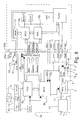
- Fig. 1 illustrates one PCMCIA interface in an electronic device as a reduced block diagram.
- the operating voltage is supplied to the PCMCIA card via two operating voltage contacts of the PCMCIA interface: V cc1 , V cc2 .
- the operating voltage can be advantageously 3.3V, 5.0V or it can be selected to be either 3.3V or 5.0V. In the case where the voltage can be selected, the selection is controlled by data in the CIS database.
- the PCMCIA interface has two programming voltage contacts V pp1 , V pp2 which are used only for programming of FLASH memory cards in known PCMCIA connections. These contacts can advantageously be set at either 0 V, 12 V or at an operating voltage V cc , according to the data in the CIS database.
- the voltage which is directed to the operating voltage contacts V cc1 , V cc2 is regulated, whereby power loss is effected in the regulator.
- the degree of the power loss is affected e.g. by the difference between the input and output voltages of the regulator and also by the current consumed by the PCMCIA card which is connected to the PCMCIA interface by the operating voltage contacts V cc1 , V cc2 .
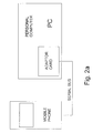
- Fig. 2a illustrates the operational blocks of the expansion card which can be connected to the expansion card connector of the PC and the operational blocks of the transmitter/receiver unit of the mobile phone.
- the operational blocks also illustrate the functional details of the units.
- the block 21 of the expansion card includes the standard interface whereby the connection to the PC is provided.
- the block 22 of the expansion card is an automatic calling module interpreting the commands, such as AT and V.25bis commands, i.e., so-called modem commands, sent from the PC to the card.
- the actual data such as a facsimile transmission, is passed from the connection block 21 to the adaptation and network service module 23 which converts the output data to the protocol required by the network service used.
- the data in the correct protocol form is passed via a bus connection 24 to a fast serial bus.
- the data coming via the serial bus enters a bus interface block 28 in a mobile phone.
- the bus interface block 28 directs the data according to the address information included in the data, either to a signalling and control block 26 or to a channel coder of the phone.
- the signalling and control block 26 is, in practice, the microprocessor of the phone.
- the channel coder of the phone is a digital signal processor DSP.
- the data is readily provided in a form that can be directly passed to the input/output port of the processors, wherein no conversions need to be made.
- the channel coder in block 25 codes both the control data from the block 26 and the traffic message from an external bus, such as a fax-message, whereby the coded information will be sent to the radio path via a radio unit 27.
- the data received from the radio path is decoded in a decoder 25.
- the decoded data is directed as control data or traffic data as such to the bus interface block 26 which adapts the data to the external bus.
- the functional steps are made in reverse order compared to the data transmission of the terminal explained above.
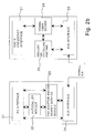
- Fig. 3 illustrates a reduced block diagram of a transmitter/receiver unit of one mobile station positioned in a prior art PCMCIA card.
- the unit controlling the operation of the card is advantageously a microcontroller 13a (MCU) having e.g. a processor, memory (RAM, ROM), and input/output lines for connecting the microprocessor to the other electronics of the card.
- MCU microcontroller 13a
- external memory 10 can be connected to the microcontroller 13a.
- a transmitter TX comprises e.g. a modulator for modulating the signal to be sent, filters in particular for attenuating spurious emissions, a mixer in which the modulated signal is mixed to the local oscillator frequency for creating a radio frequency signal, and a power amplifier for amplifying the signal to be sent.
- the amplified signal is directed to an antenna ANT, which is connected to the card e.g. by means of a cable.
- a receiver RX comprises e.g. filters for filtering the received signals, a mixer for changing the radio frequency signal to be received to an intermediate frequency or, in a direct-conversion type receiver, to a baseband, and a detector for demodulating the received signal.
- connection circuits such as a control circuit 13b (ASIC), for transferring of signals between the PC and the transmitter/receiver.
- ASIC control circuit 13b
- the transmitter/receiver unit has no power supply of its own, but the power supply is provided from the PC via the PCMCIA connection.
- the watch-dog circuit RESET of the expansion card keeps the microcontroller 13a of the card at the initial phase of the operating voltage if the operating voltage of the card is, for some reason, insufficient. Thus, malfunctions of the microcontroller are eliminated e.g. during the coupling of the voltages.
- Power consumption of the transmitter/receiver card varies during the operation.
- the power amplifier of the transmitter consumes a lot of power, wherein the power consumption is particularly high during the transmission. Since the card obtains the required operating voltage from the PC via the PCMCIA interface, the high power consumption causes the maximum current limit of the voltage contacts to be exceeded.
- the connector may be damaged if the PC or the card has no current restriction for ensuring that the current limit is not exceeded.
- the restriction of the current also restricts the initial power of the power amplifier, i.e., the intensity of the signal to be sent to the radio path. This may result in deterioration of the connection quality or even interruption of the connection.
- a high power consumption also includes the disadvantage that power losses in the current supply circuit of the PC increase, wherein a part of the power taken from the power supply of the PC turns into heat inside the PC, and, on the other hand, the operation time of the PC at a single charge decreases, because the battery runs down faster.
- An advantage of the present invention is to ameliorate the above described drawbacks and to provide an expansion card interface whereby the intensity of the current that can be supplied via the connection to the expansion card can be increased to be higher than the current in connection with prior art connections, and to decrease voltage loss between the power supply of the electronic device and the interface.
- the invention is based on the idea that instead of said signal, the voltage of the power supply is arranged to be switched to the electronic device.
- the present invention provides advantages over prior art solutions.
- voltage losses can be diminished between the power supply of the electronic device and the interface.
- the internal power consumption of the electronic device decreases, resulting in there being less heating of the electronic device is than when prior art interfaces are used. Further, higher currents can be supplied to the expansion card.
- an expansion card comprising an expansion card connector to be connected to an expansion card connector of an electronic device, said expansion card connector of the expansion card comprising a contact for transferring a given signal, and said electronic device comprising a power supply, such as a battery or a mains supply characterised in that :
- an interface wherein said interface is formed between an electronic device and an expansion card, whereby a voltage supply contact may be selectively coupled to one or other of :
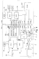
- Fig. 4 illustrates only those blocks which are necessary for the invention to be understood.
- the expansion card 1 is connected to the electronic device 2, such as a portable computer.
- the expansion card 1 can be any expansion card.
- a few connection lines are shown in Fig. 4, such as power supply lines V cc1 , V cc2 , V pp1 , V pp2 .
- the electronic device 2 obtains its operating voltage from a power supply 11, which is advantageously a battery, or a mains supply 14.
- the mains supply 14 rectifies the mains supply voltage and converts the rectified voltage to a voltage that is suitable for a current supply circuit 3, for example to +12V.
- mains supply 14 can be used for charging the battery.
- the voltage value of the power supply V batt of the electronic device is insignificant as such in view of the operation of the present invention.
- the voltage value depends on the respective electronic device used and the value of the voltage or voltages used therein. In most common embodiments, such as the PCMCIA interfaces, the voltage V batt of the power supply 11 is higher than the operating voltage V cc , but not more than +12V.
- the voltage V batt of the power supply 11 is lowered in the current supply circuit, but also voltage increasing circuits and inverters are known, with which for example a negative output voltage is provided from a positive input voltage.
- losses take place in current supply circuit, wherein a part of the power supplied by the power supply 11 turns into heat. The amount of the losses depend e.g. on the amount of the current taken from the current supply circuit, wherein losses increase as the current value increase.
- the first and second power supply line V cc1 , V cc2 , as well as the supply lines V pp1 , V pp2 for the programming voltage, are in this interface provided by means of two contacts for example for obtaining a higher current supply capacity for the expansion card 1.
- the voltage V batt is directed to a current supply circuit 3, such as a regulator, wherein, depending on the embodiment, usually several voltages of various values, e.g. 3V, 5V, 12V and -12V may be provided as the operating voltages.
- a current supply circuit 3 such as a regulator, wherein, depending on the embodiment, usually several voltages of various values, e.g. 3V, 5V, 12V and -12V may be provided as the operating voltages.
- the regulated operating voltage is directed to a buffer stage 4, where the regulated voltage or voltages are buffered, i.e., the current supply circuit is protected against spurious signals and short circuits coming through the interface.
- two current supply lines V cc , V pp start from the buffer stage 4. Switches 5, 5' are placed on these lines before the interface.
- the circuits determined for the power supply lines which circuits are, in this case, the programming voltage line Vpp and the operating voltage line V cc of the buffer stage 4, are interrupted in a manner that the circuits are not directed to the lines of said interface 33a, but to the switches 5, 5'.
- the first circuit such as the operating voltage line V cc, is directed to a first input pin 6 of the first switch 5.
- the voltage V batt of the power supply 11 of the electronic device 2 is directed via a voltage line 12 to a second input pin 7 of the first switch 5.
- the voltage line 12 is advantageously an electric wire provided at the printed circuit board, but it can further comprise for example interference suppressers, if necessary.
- An output pin 8 of the first switch 5 is connected to the first and second operating voltage contact V cc1 , V cc2 of the interface 33a.
- the second circuit, such as the programming voltage line V pp is directed to a first input pin 6' of the second switch 5'.
- the voltage V batt of the power supply 11 of the electronic device 2 is directed via the voltage line 12 to a second input pin 7' of the second switch 5'.
- An output pin 8' of the second switch 5' is connected to the first and second programming voltage contacts V pp1 , V pp2 of the interface 33a.
- a control unit 9 of the electronic device such as a microprocessor 9a and control circuit 9b, directs the first switch 5 either to a first position, where the first input pin 6 is connected to the output pin 8 of the first switch, or to a second position, where the second input pin 7 is connected to the output pin 8 of the first switch.
- the control unit 9 directs the second switch 5' either to a first position, where the first input pin 6' is connected to the output pin 8' of the second switch, or to a second position, where the second input pin 7' is connected to the output pin 8' of the second switch.
- An oscillator 29, such as a crystal oscillator, provides one or several clock signals to the control unit 9 of the electronic device.
- memory 30 is connected to the control unit 9.
- the memory comprises for example read-only memory e.g. for storing application software and random access memory for storing and reading the changing data.
- the control of the switches 5, 5' is carried out by control lines 15, 15', advantageously in a manner that at the fist value of the control line, e.g. about 0V, the switch 5, 5' is at said first position, and at the second value of the control line, e.g. about 5V, the switch 5, 5' is at said second position.
- the control can be carried out e.g. according to what is stored in the CIS database of the expansion card 1 connected to the expansion card interface 33a.
- the switches 5, 5' can be controlled also independently of each other, wherein they can be at different positions.
- the supply of operating voltages can be arranged several ways in the expansion card.
- the wiring can be fixed, wherein the operating voltage is wired from the respective operating-power supply contacts of the interface 33b in the card either to all the circuits of the card, or to those circuits whose power consumption is the highest.
- a part of the circuits can be connected e.g. to a conventional supply contact V' cc1 , V cc2 of the operating voltage corresponding to the supply contact V cc1 , V cc2 of the operating voltage and the unregulated voltage is directed via another contact, such as a contact V' pp1 , V' pp2 corresponding to the supply contact V pp1 , V pp2 of the programming voltage.
- the operating voltage V cc or the voltage V batt of the power supply 11 of the electronic device is arranged to be connected to the supply contacts V pp1 , V pp2 of the programming voltage.
- a transmitter/receiver unit TX/RX is connected to the supply contacts V' pp1 , V' pp2 of the programming voltage on the expansion card, and the rest of the electronics of the card is connected to the standard supply contacts V' cc1 , V' cc2 of the operating voltage.
- the expansion card interface of Fig. 4 can be applied also in a manner that the operating voltage V cc or the voltage V batt of the power supply 11 of the electronic device can be connected to the supply contacts V cc1 , V cc2 of the operating voltage.
- the CIS database is advantageously stored in a non-volatile random access memory (NVRAM) 10, which in this example is carried out by FLASH memory circuits.
- NVRAM non-volatile random access memory
- the CIS database is seen as memory at a given location.
- the PCMCIA standard includes a definition that the CIS database begins at an address 0 of the attribute memory.
- the reading of CIS database is carried out so that the processor of the electronic device sets the initial address of the CIS database to the address lines A0 to A15 of the card interface; the control line DIR of the transfer direction to a state where the data transfer direction of the data lines DO to D7 is from the card to the electronic device; the data buffers enable line OE to a state where data buffers DBUFF are activated; and the data reading line IORD to the reading state.
- the first byte of the CIS database can be read in the data bus of the interface by the electronic device.
- the next byte is read according to a corresponding principle, by setting the address of the next byte to the address line.
- Said states of the control lines DIR, OE, IORD depend on the respective embodiment used, and they can be active low, which is known as such, i.e., a logic 0 state (voltage value about 0V in connection with common CMOS and TTL circuits) activates the function, or active high, i.e., a logic 1 state (about a voltage corresponding to the operating voltage in connection with common CMOS and TTL circuits) activates the function.
- the switch 5 is preferably set to a first position, i.e., the first input pin 6 is connected to conduct electricity to the output pin 8. In this case the operating voltage is supplied to the card only via the current supply connection of the electronic device. However, in connection with expansion cards with a high power consumption, about 0.5 A to 1.0 A, the switch 5 is set to a second position, i.e., the second input pin 7 is connected to conduct electricity to the output pin 8, wherein the unregulated voltage V batt of the power supply 11 is directed to the expansion card. In particular with mobile station embodiments, the accuracy demand with the operating voltage of the power amplifier of the transmitter is not that high that the operating voltage should be regulated. Thus, when applying the interface of the invention, the voltage losses between the power supply of the electronic device and the expansion card interface can be reduced, in particular in connection with expansion cards with a high power consumption.
- the manufacturer of the expansion card has already at the manufacturing stage programmed the CIS database with the information that a voltage line 12 of the electronic device can be switched to the card, at one of the connector contacts.
- the electronic device can connect the operating voltage to the expansion card directly from the power supply 11, wherein the internal power losses of the electronic device can be reduced, which raises the operation time of the electronic device at one charge and also decreases heat forming in the electronic device.
- connection of the operating voltage can be controlled on the basis of the use of the CIS database or the like, it is also possible to carry out the control on the basis of the apparatus.
- An embodiment of this is shown in Fig. 5.
- one of the contacts of the expansion card connectors 33a is used, such as the voltage sense contacts VS#1, VS#2.
- the expansion card sets said contacts either to the 0 state (e.g. about 0V) or to the 1 state (e.g. about 5V) according to the fact whether the above described possibility to switch the operating voltage exists in the card.
- pull down or pull up can be utilized when carrying out the control.
- the electronic device advantageously includes an open emitter type output, which, in the coupling of Fig. 5 is carried out by an NPN transistor T, which is connected to the first voltage sense contact VS#1.
- the operating point of the transistor is set by a resistance R2 connected between the base of the transistor and the operating voltage V cc .
- the control line 15' of the switch 5' is connected to the emitter.
- the voltage level in the control line 15' is about 5V when an operating voltage of 5V is used in the circuits of the expansion card interfaces 33a.
- the switch 5' is at its first position, i.e., the operating voltage is directed to the expansion card from the power supply 11 of the electronic device via the current supply connection.
- the expansion card connected to the expansion card connector 33a includes a pull down resistance R1 connected electrically to a contact corresponding to the first voltage sense contact VS#1, the pull down resistance R1 causes the voltage to drop to about 0V in the control line 15' of the switch.
- the switch 5' is moved from one position to the other, i.e., the operating voltage is directed to the transmitter/receiver unit TX/RX in the expansion card directly from the power supply 11 of the electronic device.
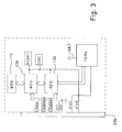
- Fig. 6 illustrates a reduced block diagram of an expansion card interface in accordance with an advantageous embodiment of the invention, wherein the electronic device 2 is a handset 16 of a telephone.
- the telephone can be e.g. a mobile station, such as a GSM mobile station.
- the handset 16 advantageously includes a microphone 19, earphone 20, display driver 17a, display 17b and keypad 18.
- the expansion card 1 can be connected to the expansion card connector 33a, e.g. by pushing it through an opening (not shown) provided in the handset 16.
- the microphone 19 is coupled to the microphone connector contact MIC of the expansion card connector 33a through a microphone amplifier 31, and the earphone 20 is coupled to the earphone connector contact EAR of the expansion card connector 33a through an earphone amplifier 32.
- the microphone and earphone lines are directed to the transmitter/receiver line TX/RX.
- the display driver 17a and the keypad 18 are connected to the control unit9, wherein the application software in the microprocessor 9a of the control unit operates such that the controls from the keypad are transferred to the expansion card 1 and, in a corresponding manner, that the display messages from the expansion card 1 are transferred via the display driver 17a to the display 17b.
- the transfer of signals can be e.g. parallel, as in the embodiment shown in Fig. 6, or also serial form data transfer can be used between the electronic device 2 and the expansion card 1.
- the operating voltage of the transmitter/receiver unit TX/RX can be selected by the second switch 5', as illustrated for example in the embodiment of Fig. 4.
- the internal power consumption in the handset 16 of the telephone can be reduced by switching the switch 5' to a second position, wherein the transmitter/receiver unit obtains its operating voltage directly from the operating power supply 11 of the handset 16.
Landscapes
- Engineering & Computer Science (AREA)
- General Engineering & Computer Science (AREA)
- Theoretical Computer Science (AREA)
- Computer Hardware Design (AREA)
- Physics & Mathematics (AREA)
- General Physics & Mathematics (AREA)
- Power Sources (AREA)
- Mobile Radio Communication Systems (AREA)
- Credit Cards Or The Like (AREA)
Applications Claiming Priority (2)
| Application Number | Priority Date | Filing Date | Title |
|---|---|---|---|
| FI964398 | 1996-10-31 | ||
| FI964398A FI104920B (fi) | 1996-10-31 | 1996-10-31 | Elektroniikkalaite, korttiliitäntä ja laajennuskortti |
Publications (2)
| Publication Number | Publication Date |
|---|---|
| EP0841608A2 true EP0841608A2 (de) | 1998-05-13 |
| EP0841608A3 EP0841608A3 (de) | 2003-01-02 |
Family
ID=8546983
Family Applications (1)
| Application Number | Title | Priority Date | Filing Date |
|---|---|---|---|
| EP97308621A Withdrawn EP0841608A3 (de) | 1996-10-31 | 1997-10-28 | Elektronische Vorrichtung, Kartenschnittstelle, und Erweiterungskarte |
Country Status (4)
| Country | Link |
|---|---|
| US (1) | US6292858B1 (de) |
| EP (1) | EP0841608A3 (de) |
| JP (1) | JPH10161783A (de) |
| FI (1) | FI104920B (de) |
Cited By (1)
| Publication number | Priority date | Publication date | Assignee | Title |
|---|---|---|---|---|
| GB2398403A (en) * | 2003-02-11 | 2004-08-18 | O2Micro Inc | A power switch for enhanced pc cards |
Families Citing this family (10)
| Publication number | Priority date | Publication date | Assignee | Title |
|---|---|---|---|---|
| US20060193278A1 (en) * | 1997-10-15 | 2006-08-31 | Wolfgang Theimer | Mobile telephone for Internet applications |
| GB2332345B (en) * | 1997-12-09 | 2002-12-11 | Sony Uk Ltd | A digital video receiver a conditional access module and a method of transmitting data therebetween |
| JP3461323B2 (ja) * | 2000-03-28 | 2003-10-27 | シャープ株式会社 | Pcカード |
| US7376769B1 (en) * | 2000-09-14 | 2008-05-20 | Intel Corporation | Wireless computing device having an application and wireless subsystem and method therefore |
| JP4517502B2 (ja) * | 2000-12-12 | 2010-08-04 | ソニー株式会社 | Icカード、icカードシステムおよびデータ処理装置 |
| JP3625187B2 (ja) * | 2000-12-18 | 2005-03-02 | シャープ株式会社 | カード型無線通信装置及びそれを用いた無線通信システム |
| JP3959374B2 (ja) * | 2003-06-30 | 2007-08-15 | Tdk株式会社 | Usbインターフェースシステム |
| JP4412947B2 (ja) * | 2003-09-08 | 2010-02-10 | 株式会社ルネサステクノロジ | メモリカード |
| CN100354845C (zh) * | 2003-10-24 | 2007-12-12 | 美国凹凸微系有限公司 | Pc卡子系统、计算机系统及操作连接至其的pc卡的方法 |
| CN103425236B (zh) * | 2012-05-15 | 2016-06-08 | 联发科技股份有限公司 | 具备多用途接口的装置 |
Family Cites Families (29)
| Publication number | Priority date | Publication date | Assignee | Title |
|---|---|---|---|---|
| US5392282A (en) | 1989-05-17 | 1995-02-21 | Nokia Mobile Phones, Ltd. | Circuit arrangement in a mobile phone for a digital mobile telephone system |
| US5241284A (en) | 1990-02-16 | 1993-08-31 | Nokia Mobile Phones Ltd. | Circuit arrangement for connecting RF amplifier and supply voltage filter |
| FI87033C (fi) | 1990-10-05 | 1992-11-10 | Nokia Mobile Phones Ltd | Foerfarande foer att arrangera styrningar av kopplingstyp i en radiotelefon |
| FI88657C (fi) | 1991-02-12 | 1993-06-10 | Nokia Mobile Phones Ltd | Foerfarande foer att minska stroemfoerbrukningen i en mobiltelefon |
| EP0522720B1 (de) | 1991-06-18 | 1999-08-18 | Nokia Mobile Phones Ltd. | Einstellung der Taktfrequenz einer elektrischen Schaltung |
| FI89223C (fi) | 1991-10-03 | 1993-08-25 | Nokia Mobile Phones Ltd | Digitalt audiointerface i gsm-anordning |
| FR2686172B1 (fr) * | 1992-01-14 | 1996-09-06 | Gemplus Card Int | Carte enfichable pour microordinateur formant lecteur de carte a contacts affleurants. |
| JPH0821015B2 (ja) * | 1992-01-20 | 1996-03-04 | インターナショナル・ビジネス・マシーンズ・コーポレイション | コンピュータならびにそのシステム再構成化装置および方法 |
| FI98183C (fi) | 1992-02-14 | 1997-04-25 | Nokia Mobile Phones Ltd | Järjestely data-adapterin kytkemiseksi GSM-solukkopuhelimeen |
| FI95980C (fi) | 1992-09-04 | 1996-04-10 | Nokia Mobile Phones Ltd | Menetelmä ja kytkentäjärjestely ajan mittaamiseksi tarkasti epätarkalla kellolla |
| US5512886A (en) * | 1992-10-19 | 1996-04-30 | Motorola, Inc. | Selective call receiver with computer interface |
| JP3477781B2 (ja) * | 1993-03-23 | 2003-12-10 | セイコーエプソン株式会社 | Icカード |
| FI97765C (fi) | 1993-11-26 | 1997-02-10 | Nokia Mobile Phones Ltd | Menetelmä sekä kytkentäjärjestely kutsuviestien käsittelemiseksi matkaviestimessä |
| US5471655A (en) | 1993-12-03 | 1995-11-28 | Nokia Mobile Phones Ltd. | Method and apparatus for operating a radiotelephone in an extended stand-by mode of operation for conserving battery power |
| US5491718A (en) | 1994-01-05 | 1996-02-13 | Nokia Mobile Phones Ltd. | CDMA radiotelephone having optimized slotted mode and long code operation |
| US5519851A (en) * | 1994-03-14 | 1996-05-21 | Sun Microsystems, Inc. | Portable PCMCIA interface for a host computer |
| FI941221A7 (fi) | 1994-03-15 | 1995-09-16 | Nokia Corp | Menetelmä matkaviestinjärjestelmän radiopuhelimen tehonkulutuksen pienentämiseksi ja matkaviestin |
| US5664118A (en) * | 1994-03-28 | 1997-09-02 | Kabushiki Kaisha Toshiba | Computer system having detachable expansion unit |
| US5701515A (en) * | 1994-06-16 | 1997-12-23 | Apple Computer, Inc. | Interface for switching plurality of pin contacts to transmit data line and plurality of pin contacts to receive data line to interface with serial controller |
| US5650973A (en) | 1994-09-27 | 1997-07-22 | Micrel, Inc. | PCMCIA power multiplexer integrated circuit with programmable decode |
| FI97262C (fi) | 1994-10-03 | 1996-11-11 | Nokia Mobile Phones Ltd | Tulosignaalin kynnysarvon ylityksen virtaa säästävä ilmaisu |
| US5613130A (en) * | 1994-11-10 | 1997-03-18 | Vadem Corporation | Card voltage switching and protection |
| US5514995A (en) * | 1995-01-30 | 1996-05-07 | Micrel, Inc. | PCMCIA power interface |
| US5589719A (en) * | 1995-03-10 | 1996-12-31 | Fiset; Peter D. | Card out of socket detector for IC cards |
| JP2986375B2 (ja) * | 1995-06-22 | 1999-12-06 | インターナショナル・ビジネス・マシーンズ・コーポレイション | 情報処理装置及びその制御方法 |
| US5613235A (en) | 1995-06-29 | 1997-03-18 | Nokia Mobile Phones Limited | Operation of a radiotelephone in a synchronous extended standby mode for conserving battery power |
| FI111309B (fi) * | 1996-01-03 | 2003-06-30 | Nokia Corp | Tietoliikenneverkkoon radioteitse liitettävä päätelaite |
| US6044472A (en) * | 1996-06-21 | 2000-03-28 | Archos | Device and method for supplying power to an external data medium reader unit connected to a computer, and external reader unit including this device |
| US5847553A (en) * | 1996-09-09 | 1998-12-08 | Sierra Wireless, Inc. | Current booster for PC card |
-
1996
- 1996-10-31 FI FI964398A patent/FI104920B/fi not_active IP Right Cessation
-
1997
- 1997-10-28 US US08/958,841 patent/US6292858B1/en not_active Expired - Fee Related
- 1997-10-28 EP EP97308621A patent/EP0841608A3/de not_active Withdrawn
- 1997-10-30 JP JP9299007A patent/JPH10161783A/ja active Pending
Non-Patent Citations (1)
| Title |
|---|
| 1995, MINDSHARE INC, ANDERSON D, PCMCIA SYSTEM ARCHITECTURE. 16-BIT PC CARDS * |
Cited By (3)
| Publication number | Priority date | Publication date | Assignee | Title |
|---|---|---|---|---|
| GB2398403A (en) * | 2003-02-11 | 2004-08-18 | O2Micro Inc | A power switch for enhanced pc cards |
| GB2398403B (en) * | 2003-02-11 | 2005-06-01 | O2Micro Inc | Enhanced power switch device enabling modular USB PC cards |
| US7365454B2 (en) | 2003-02-11 | 2008-04-29 | O2Micro International Limited | Enhanced power switch device enabling modular USB PC cards |
Also Published As
| Publication number | Publication date |
|---|---|
| US6292858B1 (en) | 2001-09-18 |
| FI964398A0 (fi) | 1996-10-31 |
| FI104920B (fi) | 2000-04-28 |
| JPH10161783A (ja) | 1998-06-19 |
| FI964398L (fi) | 1998-05-01 |
| EP0841608A3 (de) | 2003-01-02 |
Similar Documents
| Publication | Publication Date | Title |
|---|---|---|
| US5655092A (en) | Multiple element interface | |
| US5797102A (en) | Arrangement for adapting the signal level in mobile phones | |
| US6452402B1 (en) | Apparatus for determining the type of external device being connected | |
| US6336039B1 (en) | IC card-type radio communication device | |
| US5649001A (en) | Method and apparatus for adapting a communication interface device to multiple networks | |
| US6285706B1 (en) | Modem having separate modem engine and data access arrangement | |
| US5712977A (en) | Method and apparatus for initial country selection in a universal modem with cable | |
| US6507610B1 (en) | Cordless modem system having multiple base and remote stations which are interusable and secure | |
| EP0841608A2 (de) | Elektronische Vorrichtung, Kartenschnittstelle, und Erweiterungskarte | |
| JPH07321964A (ja) | 電話回線源の電源及び電話通信装置 | |
| US6088746A (en) | Mode selection line for selecting one of a plurality of operation modes said selection line can also be used for original purpose after mode selection | |
| US8544752B2 (en) | Nonvolatile memory card adaptable to plural specifications | |
| US20080012524A1 (en) | Chargeable electronic devices and direct current voltage supply systems | |
| EP0919932A2 (de) | Erweiterungskarte | |
| US6184592B1 (en) | System and method for supplying power to an expansion card | |
| US6420898B2 (en) | Input/output buffer capable of supporting a multiple of transmission logic buses | |
| JP2002116853A (ja) | Usb搭載電子機器及びそれに用いるusbケーブル | |
| US20060293082A1 (en) | Extension of the sim card in gsm devices | |
| US20070283053A1 (en) | Memory card with communication serial interface | |
| EP0918399A1 (de) | Telekommunikationskarte | |
| CA2147119A1 (en) | Modem for selectively connecting to a land line or to a cellular telephone | |
| CN220254683U (zh) | 网卡 | |
| CN220526325U (zh) | 一种接口检测电路及终端设备 | |
| CN217655451U (zh) | 用于实现通讯切换的控制电路及照明控制系统 | |
| CN221125244U (zh) | 一种usb接口电路 |
Legal Events
| Date | Code | Title | Description |
|---|---|---|---|
| PUAI | Public reference made under article 153(3) epc to a published international application that has entered the european phase |
Free format text: ORIGINAL CODE: 0009012 |
|
| AK | Designated contracting states |
Kind code of ref document: A2 Designated state(s): AT BE CH DE DK ES FI FR GB GR IE IT LI LU MC NL PT SE |
|
| RAP1 | Party data changed (applicant data changed or rights of an application transferred) |
Owner name: NOKIA CORPORATION |
|
| PUAL | Search report despatched |
Free format text: ORIGINAL CODE: 0009013 |
|
| AK | Designated contracting states |
Kind code of ref document: A3 Designated state(s): AT BE CH DE DK ES FI FR GB GR IE IT LI LU MC NL PT SE |
|
| 17P | Request for examination filed |
Effective date: 20030625 |
|
| AKX | Designation fees paid |
Designated state(s): DE FR GB SE |
|
| 17Q | First examination report despatched |
Effective date: 20050520 |
|
| STAA | Information on the status of an ep patent application or granted ep patent |
Free format text: STATUS: THE APPLICATION IS DEEMED TO BE WITHDRAWN |
|
| 18D | Application deemed to be withdrawn |
Effective date: 20051001 |