EP0841620A1 - Carte mère avec configuration automatique - Google Patents
Carte mère avec configuration automatique Download PDFInfo
- Publication number
- EP0841620A1 EP0841620A1 EP96309286A EP96309286A EP0841620A1 EP 0841620 A1 EP0841620 A1 EP 0841620A1 EP 96309286 A EP96309286 A EP 96309286A EP 96309286 A EP96309286 A EP 96309286A EP 0841620 A1 EP0841620 A1 EP 0841620A1
- Authority
- EP
- European Patent Office
- Prior art keywords
- cpu
- motherboard
- reset
- multiplier
- parameters
- Prior art date
- Legal status (The legal status is an assumption and is not a legal conclusion. Google has not performed a legal analysis and makes no representation as to the accuracy of the status listed.)
- Withdrawn
Links
Images

Classifications
-
- G—PHYSICS
- G06—COMPUTING OR CALCULATING; COUNTING
- G06F—ELECTRIC DIGITAL DATA PROCESSING
- G06F9/00—Arrangements for program control, e.g. control units
- G06F9/06—Arrangements for program control, e.g. control units using stored programs, i.e. using an internal store of processing equipment to receive or retain programs
- G06F9/44—Arrangements for executing specific programs
- G06F9/4401—Bootstrapping
- G06F9/4403—Processor initialisation
-
- G—PHYSICS
- G06—COMPUTING OR CALCULATING; COUNTING
- G06F—ELECTRIC DIGITAL DATA PROCESSING
- G06F13/00—Interconnection of, or transfer of information or other signals between, memories, input/output devices or central processing units
- G06F13/38—Information transfer, e.g. on bus
- G06F13/40—Bus structure
- G06F13/4063—Device-to-bus coupling
- G06F13/4068—Electrical coupling
- G06F13/4072—Drivers or receivers
Definitions
- the present invention relates to a motherboard for a personal computer that automatically configures itself for the speed, multiplier and voltage required for the type of microprocessor, (CPU), installed in the motherboard.
- CPU microprocessor
- the present invention is a logic circuit and a special module of BIOS for a computer motherboard that automatically reconfigures the motherboard to accept different microprocessors, (CPUs).
- CPUs microprocessors
- Each series of CPUs, (486, Pentium, Pentium Pro, etc.) includes different types having different parameters including: manufacturers, (Intel, AMD, Cyrix, etc.); basic frequencies, (50MHz, 60MHz, 66MHz, 75MHz, etc.) multipliers, (1.5X, 2.0X, 2.5X, 3.0X, etc.); and operating voltages, (3.3V, 2.8V, etc.).
- manufacturers Intel, AMD, Cyrix, etc.
- basic frequencies 50MHz, 60MHz, 66MHz, 75MHz, etc.
- multipliers (1.5X, 2.0X, 2.5X, 3.0X, etc.)
- operating voltages (3.3V, 2.8V, etc.).
- these different parameters must be set on a conventional motherboard by opening and closing jumpers and/or dip-switches.
- the operating system senses whether a "hot key”, (this can be preprogrammed to be any of the keys on the keyboard), is being or has been pressed.
- a hot key this can be preprogrammed to be any of the keys on the keyboard
- the computer enters BIOS setup and the operator can then change the CPU parameters, (voltage, frequency and multiplier), as displayed on the screen. If the hot key is not pressed, the computer simply uses the parameters as previously defined.
- the BIOS can be entered from resets other than power-up and the CPU configuration can be changed without turning the computer off.
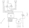
- Fig. 1 is a circuit diagram of the control logic used to set the CPU frequency, multiplier and voltage in accordance with the present invention.
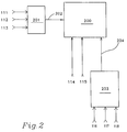
- Fig. 2 is a circuit diagram of the CPU, voltage generator and clock chip as controlled by the present invention.
- Fig. 3 is a flow chart of the BIOS operation used to set the CPU frequency, multiplier and voltage in accordance with the present invention.
- Fig. 4 is a circuit diagram of the CPU, voltage generator and clock chip as controlled by jumpers in prior art motherboards.
- the present invention is drawn to configuring a computer motherboard to operate with a specific microprocessor.
- the operating voltage, frequency and multiplier are selected by physically changing jumpers or dip-switches on the motherboard.
- Figure 4 shows one type of prior art circuit used to accomplish this.
- a microprocessor 400 has inputs for an operating voltage 402 , multiplier selectors 406 , (BF-1 and BF-2), and a CPU clock 408 .
- the operating voltage is provided by a CPU voltage generator 401 that determines the proper voltage by reading three inputs 404 , (VCC2A, VCC2B, and VCC3).
- the CPU clock input 408 operates at a frequency determined by reading three inputs 407 , (SEL1, SEL2 and SEL3).
- the multiplier selectors 406 , voltage determining inputs 404 and frequency determining inputs 407 are tied to ground using jumpers, (or closing dip-switches), to provide logic low levels. For inputs that require a logic high level, the jumpers are removed, (or the dip-switches are opened), and pull-up resisters 405 provide V cc potential. High-low combinations of these inputs select the various functions as listed in Table 1 below.
- FIG 4 While the circuit shown in figure 4 is prior art, the present invention uses the same setup as the microprocessor, CPU clock and CPU voltage generator. The difference between the prior art circuit and the circuit of the present invention can be seen by viewing figure 2.
- This circuit includes a microprocessor 200 , a CPU clock 203 and a CPU voltage generator 201 , however, it should be noted that the jumpers, (or dip-switches) and the pull-up resisters 405 have been eliminated as unnecessary for the circuit of the present invention.
- SEL1, SEL2 and SEL3 are listed in figure 2 as 116-118 respectively, BF1 and BF2 are listed as 115 and 114 respectively, and VCC2A, VCC2B and VCC3 are listed as 113-111 respectively.
- the CPU voltage generator supplies the CPU with operating voltage at line 202
- the CPU clock supplies the clock frequency at line 204 .
- Data latches 101 are connected to eleven of the computer data lines 106 that provide the programming information when the CPU 200 is prompted by the BIOS program.
- a decoder 102 triggers the data latches 101 when the correct address is provided via address line 107 .
- Lines 108 and 109 are WR and RD respectively and are also used by the CPU 200 and BIOS to prompt the decoder 102 to download the data lines' information via the data latches 101 for reconfiguration.
- the decoder 102 also triggers solid state relay 105 by providing a logic low level to the control port of the solid state relay 105 .
- Solid state relay 105 When the solid state relay 105 is triggered it provides a "data in" signal at 110 to the CPU which signals the CPU that the new parameters have been provided at lines 111-118 , and assists in testing the reset status.
- Two additional solid state relays, 103 and 104 are provided on the 114 and 115 lines, (BF2 and BF1 respectively), and these relays operate in a similar manner to solid state relay 105 , and are triggered by two of the eleven data lines, (after being latched by data latches 101 ).
- Solid state relays 103-105 are necessary because several other devices also drive the data in, BF1 and BF2 lines, and these devices insure that two devices do not attempt to drive the same line at the same time.
- FIG. 3 is a flow chart explaining the operation of the BIOS software used to configure the motherboard via the control logic explained above.
- Any type of reset (system power on, system reset and CPU reset), will initialize the BIOS at "Start" block 300 .
- the system then proceeds to the Initialization block 301 where certain system components are reset, (depending on the type of reset as is well known in the art), such as clearing RAM, spinning up any hard drives, etc.
- the system proceeds to block 302 , where it is determined if the reset was caused by powering up the computer. At this point we will consider that the reset was caused by powering up the computer, (as would be necessary when replacing the CPU), and following the "Yes" line the system proceeds to block 303 .
- BIOS setup subroutine is entered and the BIOS screen is displayed on the PC's monitor, (as is well known in the art).
- BIOS screen of the present invention has blocks for entering the CPU frequency, multiplier and voltage as discussed in detail above.
- the CPU saves these parameters, block 306 , by using the CMOS RAM of the motherboard and the data latches 101 as explained above.
- the system resets, a "Speed Easy” reset as named by the inventor, at block 307 and the system returns to block 300 .
- block 308 the previously defined parameters, (stored in the CMOS RAM), are used to operate the CPU.
- the system then proceeds to block 309 which gives a standard reset and returns the system to block 300 .
- BIOS setup is not of a power up type, (system reset, CPU reset, or Speed Easy reset). If the reset is not of a power up type, (system reset, CPU reset, or Speed Easy reset), the system proceeds from block 302 to block 310 .
- the operator is given the option to enter BIOS setup as is standard in conventional computer systems, (usually by pressing the DEL key during boot-up). If the operator enters BIOS setup, the system proceeds from block 310 to block 311 , and the BIOS setup continues through blocks 312-314 as explained above for blocks 305-307 . It should be noted that whenever BIOS setup is entered, blocks 304 and 311 , not only can the parameters for the CPU be changed, but all of the standard computer parameters, (RAM, I/O ports, etc.), can be changed as is well known in the PC art.
- BIOS setup is not entered, the system proceeds from block 310 to block 315 where the processor is reset. After the processor is reset, (not to be confused with CPU reset), the system proceeds to block 316 , the boot up sequence is completed, and the disc operating system, DOS, is entered. From the above information, it can be seen that a power on reset without intervention on the part of the operator, will proceed as follows: block 300 to block 301 to block 302 to block 303 to block 308 to block 309 to block 300 to block 301 to block 302 to block 310 to block 315 to block 316 .
- a non-power up reset (pressing the system reset button on the computer case, or pressing control, ALT and DEL keys simultaneously for a CPU reset), without further intervention on the part of the operator, will proceed as follows: block 300 to block 301 to block 302 to block 310 to block 315 to block 316.
- the above invention is not limited to a complete motherboard, but may be retro-fitted on an existing motherboard by use of a module containing the circuitry of figures 1 and 2. In either case the systems BIOS program must be replaced with the BIOS program of the present invention.
Landscapes
- Engineering & Computer Science (AREA)
- Theoretical Computer Science (AREA)
- General Engineering & Computer Science (AREA)
- Software Systems (AREA)
- Physics & Mathematics (AREA)
- General Physics & Mathematics (AREA)
- Computer Hardware Design (AREA)
- Computer Security & Cryptography (AREA)
- Stored Programmes (AREA)
- Power Sources (AREA)
Applications Claiming Priority (2)
| Application Number | Priority Date | Filing Date | Title |
|---|---|---|---|
| US739727 | 1985-05-31 | ||
| US08/739,727 US5862351A (en) | 1996-11-07 | 1996-11-07 | Motherboard with automatic configuration |
Publications (1)
| Publication Number | Publication Date |
|---|---|
| EP0841620A1 true EP0841620A1 (fr) | 1998-05-13 |
Family
ID=24973529
Family Applications (1)
| Application Number | Title | Priority Date | Filing Date |
|---|---|---|---|
| EP96309286A Withdrawn EP0841620A1 (fr) | 1996-11-07 | 1996-12-19 | Carte mère avec configuration automatique |
Country Status (2)
| Country | Link |
|---|---|
| US (1) | US5862351A (fr) |
| EP (1) | EP0841620A1 (fr) |
Cited By (4)
| Publication number | Priority date | Publication date | Assignee | Title |
|---|---|---|---|---|
| EP1103892A1 (fr) * | 1999-11-24 | 2001-05-30 | Pro Team Computer Corporation | Carte d'interface prioritaire pour carte mère avec BIOS endommagé |
| DE19800187C2 (de) * | 1997-12-01 | 2003-10-30 | Micro Star Internat Co | Verfahren und Vorrichtung zum Einstecken und sofortigen Betreiben einer CPU |
| DE10323012B4 (de) * | 2003-05-21 | 2005-06-02 | Austriamicrosystems Ag | Programmierbare, integrierte Schaltungsanordnung und Verfahren zur Programmierung einer integrierten Schaltungsanordnung |
| CN111697791A (zh) * | 2020-06-22 | 2020-09-22 | 上海大因多媒体技术有限公司 | 一种集中供电装置 |
Families Citing this family (22)
| Publication number | Priority date | Publication date | Assignee | Title |
|---|---|---|---|---|
| US6718319B1 (en) * | 1996-12-03 | 2004-04-06 | Strategic Analysis, Incorporated | Method and apparatus for formatting smart cards and card readers |
| US6295567B1 (en) * | 1998-01-26 | 2001-09-25 | Dell Usa, L.P. | Chassis type determination in an electronic system |
| TW374872B (en) * | 1998-06-06 | 1999-11-21 | Via Tech Inc | Device and method for simplification of motherboard jumper and the CPU |
| TW382089B (en) * | 1998-06-16 | 2000-02-11 | Asustek Comp Inc | System clock frequency switching device and method for computer motherboard |
| US6327663B2 (en) * | 1998-10-21 | 2001-12-04 | Advanced Micro Devices, Inc. | System and method for processor dual voltage detection and over stress protection |
| US6516373B1 (en) * | 1999-06-18 | 2003-02-04 | Samsung Electronics Co., Ltd. | Common motherboard interface for processor modules of multiple architectures |
| US6772328B1 (en) * | 1999-06-18 | 2004-08-03 | Samsung Electronics Co., Ltd. | Dynamic initialization of processor module via motherboard interface |
| US6931523B1 (en) | 1999-12-09 | 2005-08-16 | Gateway Inc. | System and method for re-storing stored known-good computer configuration via a non-interactive user input device without re-booting the system |
| JP2001195237A (ja) * | 2000-01-12 | 2001-07-19 | Fujitsu Ltd | コンピュータ及びコンピュータの表示方法及びコンピュータの表示プログラムを記録した記録媒体 |
| US6668318B1 (en) * | 2000-05-31 | 2003-12-23 | Xybernaut Corp. | System and method for loading one of a plurality of operating systems and adjusting the operating frequency accordingly using transferable core computer that recognizes a system environment |
| TW563012B (en) * | 2000-11-20 | 2003-11-21 | Via Tech Inc | System and method for automatically reading the clock doubling factor of system bus |
| US6874083B2 (en) * | 2000-12-22 | 2005-03-29 | Intel Corporation | Method and apparatus to ensure proper voltage and frequency configuration signals are defined before applying power to processor |
| US6825634B2 (en) | 2001-01-18 | 2004-11-30 | Lockeed Martin Corporation | System and method for a scalable motion controller for controlling a plurality of servo motors |
| GB2383151A (en) * | 2001-12-14 | 2003-06-18 | Inventec Corp | Automatic keyboard bios updating method |
| US20060123220A1 (en) * | 2004-12-02 | 2006-06-08 | International Business Machines Corporation | Speech recognition in BIOS |
| US20060214917A1 (en) * | 2005-03-23 | 2006-09-28 | Inventec Corporation | Key function switching method and system |
| US8661233B2 (en) | 2011-03-30 | 2014-02-25 | Hewlett-Packard Development Company, L.P. | System configuration |
| CN102830751A (zh) * | 2011-06-15 | 2012-12-19 | 鸿富锦精密工业(深圳)有限公司 | 主机板 |
| TWI443495B (zh) * | 2011-09-08 | 2014-07-01 | Asustek Comp Inc | 電腦裝置及中央處理器的頻率調整方法 |
| US11320885B2 (en) * | 2020-05-26 | 2022-05-03 | Dell Products L.P. | Wide range power mechanism for over-speed memory design |
| JP2022081090A (ja) * | 2020-11-19 | 2022-05-31 | レノボ・シンガポール・プライベート・リミテッド | 情報処理装置、及び制御方法 |
| CN116414211A (zh) * | 2022-12-30 | 2023-07-11 | 苏州浪潮智能科技有限公司 | 频率控制方法、装置、系统及可读存储介质 |
Citations (7)
| Publication number | Priority date | Publication date | Assignee | Title |
|---|---|---|---|---|
| US4967346A (en) | 1988-03-14 | 1990-10-30 | Advanced Micro Devices, Inc. | Universal microprocessor interface circuit |
| EP0510241A2 (fr) | 1991-04-22 | 1992-10-28 | Acer Incorporated | Ordinateur améliorable et dégradable |
| WO1993008532A2 (fr) * | 1991-10-18 | 1993-04-29 | Epson Portland, Inc. | Stockage de programmes d'un systeme d'entree/sortie de base sur une carte mere pour une variete de types d'unites centrales d'ordinateur |
| GB2271446A (en) | 1992-04-29 | 1994-04-13 | Hany Neoman | User-built and upgradable personal computer |
| US5371892A (en) | 1989-12-19 | 1994-12-06 | 3Com Corporation | Method for configuring a computer bus adapter circuit board without the use of jumpers or switches |
| US5551012A (en) * | 1991-04-22 | 1996-08-27 | Acer Incorporated | Single socket upgradeable computer motherboard with automatic detection and socket reconfiguration for inserted CPU chip |
| WO1996038774A1 (fr) * | 1995-06-01 | 1996-12-05 | Ast Research, Inc. | Module pour uc de mise a niveau pourvu d'une alimentation integree |
Family Cites Families (4)
| Publication number | Priority date | Publication date | Assignee | Title |
|---|---|---|---|---|
| US5086501A (en) * | 1989-04-17 | 1992-02-04 | Motorola, Inc. | Computing system with selective operating voltage and bus speed |
| US5594874A (en) * | 1993-09-30 | 1997-01-14 | Cirrus Logic, Inc. | Automatic bus setting, sensing and switching interface unit |
| EP0683448B1 (fr) * | 1994-05-10 | 2002-01-09 | Intel Corporation | Procédé et dispositif de transfert synchrone de données entre dispositifs digitaux qui ont un rapport de fréquence de travail P/O entier |
| CN1106609C (zh) * | 1994-05-18 | 2003-04-23 | 英特尔公司 | 在一个计算机系统中配置多个媒体的方法和设备 |
-
1996
- 1996-11-07 US US08/739,727 patent/US5862351A/en not_active Expired - Fee Related
- 1996-12-19 EP EP96309286A patent/EP0841620A1/fr not_active Withdrawn
Patent Citations (7)
| Publication number | Priority date | Publication date | Assignee | Title |
|---|---|---|---|---|
| US4967346A (en) | 1988-03-14 | 1990-10-30 | Advanced Micro Devices, Inc. | Universal microprocessor interface circuit |
| US5371892A (en) | 1989-12-19 | 1994-12-06 | 3Com Corporation | Method for configuring a computer bus adapter circuit board without the use of jumpers or switches |
| EP0510241A2 (fr) | 1991-04-22 | 1992-10-28 | Acer Incorporated | Ordinateur améliorable et dégradable |
| US5551012A (en) * | 1991-04-22 | 1996-08-27 | Acer Incorporated | Single socket upgradeable computer motherboard with automatic detection and socket reconfiguration for inserted CPU chip |
| WO1993008532A2 (fr) * | 1991-10-18 | 1993-04-29 | Epson Portland, Inc. | Stockage de programmes d'un systeme d'entree/sortie de base sur une carte mere pour une variete de types d'unites centrales d'ordinateur |
| GB2271446A (en) | 1992-04-29 | 1994-04-13 | Hany Neoman | User-built and upgradable personal computer |
| WO1996038774A1 (fr) * | 1995-06-01 | 1996-12-05 | Ast Research, Inc. | Module pour uc de mise a niveau pourvu d'une alimentation integree |
Cited By (5)
| Publication number | Priority date | Publication date | Assignee | Title |
|---|---|---|---|---|
| DE19800187C2 (de) * | 1997-12-01 | 2003-10-30 | Micro Star Internat Co | Verfahren und Vorrichtung zum Einstecken und sofortigen Betreiben einer CPU |
| EP1103892A1 (fr) * | 1999-11-24 | 2001-05-30 | Pro Team Computer Corporation | Carte d'interface prioritaire pour carte mère avec BIOS endommagé |
| DE10323012B4 (de) * | 2003-05-21 | 2005-06-02 | Austriamicrosystems Ag | Programmierbare, integrierte Schaltungsanordnung und Verfahren zur Programmierung einer integrierten Schaltungsanordnung |
| US7724167B2 (en) | 2003-05-21 | 2010-05-25 | Austriamicrosystems Ag | Integrated circuit arrangement, and method for programming an integrated circuit arrangement |
| CN111697791A (zh) * | 2020-06-22 | 2020-09-22 | 上海大因多媒体技术有限公司 | 一种集中供电装置 |
Also Published As
| Publication number | Publication date |
|---|---|
| US5862351A (en) | 1999-01-19 |
Similar Documents
| Publication | Publication Date | Title |
|---|---|---|
| US5862351A (en) | Motherboard with automatic configuration | |
| KR100334857B1 (ko) | 슬롯 구성에 따라 디바이스 버스 속도를 변경하는 디바이스 버스 동작 방법 및 그 장치 | |
| US6631520B1 (en) | Method and apparatus for changing execution code for a microcontroller on an FPGA interface device | |
| EP0496535B1 (fr) | Configuration automatique de dispositif pour ordinateur expansible | |
| US6560665B1 (en) | Embedding firmware for a microprocessor with configuration data for a field programmable gate array | |
| US6351809B1 (en) | Method of disguising a USB port connection | |
| US6237048B1 (en) | Adapter card with vendor unique differentiation and customization using PCI sideband signals | |
| US5991875A (en) | System configuration card | |
| US6094063A (en) | Method for level shifting logic signal voltage levels | |
| US5574866A (en) | Method and apparatus for providing a data write signal with a programmable duration | |
| EP0990973B1 (fr) | Procédé et dispositif pour faciliter l'insertion et l'enlèvement de modules dans un système ordinateur | |
| US5968140A (en) | System for configuring a device where stored configuration information is asserted at a first time and external operational data is asserted at a second time | |
| US6457137B1 (en) | Method for configuring clock ratios in a microprocessor | |
| JPH11259380A (ja) | コンピュ―タ・システムのscsiデュプレクス兼用バックプレ―ン | |
| US7099966B2 (en) | Point-to-point electrical loading for a multi-drop bus | |
| KR100216870B1 (ko) | 컴퓨터의 바이오스 공용 장치 및 공용 방법 | |
| US5572718A (en) | Mechanism for dynamically determining and distributing computer system clocks | |
| US6148397A (en) | CPU plug-and-play method and device | |
| CN1081364C (zh) | 自动设置cpu参数值的个人计算机 | |
| US5377358A (en) | Character processing device adapted to perform document-editing processing and typewriting processing | |
| EP0903671B1 (fr) | Circuit d'alarme sonore pour une connexion PCI enfichable sous tension | |
| US6487618B1 (en) | Method for resisting an FPGA interface device | |
| JP2000085107A (ja) | インキ供給量設定装置 | |
| EP0326102A2 (fr) | Méthode et appareil pour sélectionner un clavier dans un système informatique | |
| KR100227513B1 (ko) | 컴퓨터의 주변장치 연결 방법 및 그 장치 |
Legal Events
| Date | Code | Title | Description |
|---|---|---|---|
| PUAI | Public reference made under article 153(3) epc to a published international application that has entered the european phase |
Free format text: ORIGINAL CODE: 0009012 |
|
| AK | Designated contracting states |
Kind code of ref document: A1 Designated state(s): DE ES FR GB IT PT |
|
| AX | Request for extension of the european patent |
Free format text: AL;LT;LV;RO;SI |
|
| 17P | Request for examination filed |
Effective date: 19981113 |
|
| AKX | Designation fees paid |
Free format text: DE ES FR GB IT PT |
|
| RBV | Designated contracting states (corrected) |
Designated state(s): DE ES FR GB IT PT |
|
| 17Q | First examination report despatched |
Effective date: 19991109 |
|
| STAA | Information on the status of an ep patent application or granted ep patent |
Free format text: STATUS: THE APPLICATION IS DEEMED TO BE WITHDRAWN |
|
| 18D | Application deemed to be withdrawn |
Effective date: 20000720 |