EP0841633A2 - Porteur d'informations portable sous la forme d'une carte avec un dispositif d'affichage optique - Google Patents
Porteur d'informations portable sous la forme d'une carte avec un dispositif d'affichage optique Download PDFInfo
- Publication number
- EP0841633A2 EP0841633A2 EP97118387A EP97118387A EP0841633A2 EP 0841633 A2 EP0841633 A2 EP 0841633A2 EP 97118387 A EP97118387 A EP 97118387A EP 97118387 A EP97118387 A EP 97118387A EP 0841633 A2 EP0841633 A2 EP 0841633A2
- Authority
- EP
- European Patent Office
- Prior art keywords
- data carrier
- card
- portable
- display device
- information
- Prior art date
- Legal status (The legal status is an assumption and is not a legal conclusion. Google has not performed a legal analysis and makes no representation as to the accuracy of the status listed.)
- Granted
Links
Images


Classifications
-
- G—PHYSICS
- G06—COMPUTING OR CALCULATING; COUNTING
- G06K—GRAPHICAL DATA READING; PRESENTATION OF DATA; RECORD CARRIERS; HANDLING RECORD CARRIERS
- G06K19/00—Record carriers for use with machines and with at least a part designed to carry digital markings
- G06K19/06—Record carriers for use with machines and with at least a part designed to carry digital markings characterised by the kind of the digital marking, e.g. shape, nature, code
- G06K19/067—Record carriers with conductive marks, printed circuits or semiconductor circuit elements, e.g. credit or identity cards also with resonating or responding marks without active components
- G06K19/07—Record carriers with conductive marks, printed circuits or semiconductor circuit elements, e.g. credit or identity cards also with resonating or responding marks without active components with integrated circuit chips
- G06K19/077—Constructional details, e.g. mounting of circuits in the carrier
- G06K19/07701—Constructional details, e.g. mounting of circuits in the carrier the record carrier comprising an interface suitable for human interaction
- G06K19/07703—Constructional details, e.g. mounting of circuits in the carrier the record carrier comprising an interface suitable for human interaction the interface being visual
-
- G—PHYSICS
- G06—COMPUTING OR CALCULATING; COUNTING
- G06K—GRAPHICAL DATA READING; PRESENTATION OF DATA; RECORD CARRIERS; HANDLING RECORD CARRIERS
- G06K19/00—Record carriers for use with machines and with at least a part designed to carry digital markings
- G06K19/04—Record carriers for use with machines and with at least a part designed to carry digital markings characterised by the shape
- G06K19/041—Constructional details
-
- G—PHYSICS
- G06—COMPUTING OR CALCULATING; COUNTING
- G06K—GRAPHICAL DATA READING; PRESENTATION OF DATA; RECORD CARRIERS; HANDLING RECORD CARRIERS
- G06K19/00—Record carriers for use with machines and with at least a part designed to carry digital markings
- G06K19/06—Record carriers for use with machines and with at least a part designed to carry digital markings characterised by the kind of the digital marking, e.g. shape, nature, code
- G06K19/06187—Record carriers for use with machines and with at least a part designed to carry digital markings characterised by the kind of the digital marking, e.g. shape, nature, code with magnetically detectable marking
- G06K19/06196—Constructional details
-
- G—PHYSICS
- G06—COMPUTING OR CALCULATING; COUNTING
- G06K—GRAPHICAL DATA READING; PRESENTATION OF DATA; RECORD CARRIERS; HANDLING RECORD CARRIERS
- G06K19/00—Record carriers for use with machines and with at least a part designed to carry digital markings
- G06K19/06—Record carriers for use with machines and with at least a part designed to carry digital markings characterised by the kind of the digital marking, e.g. shape, nature, code
- G06K19/067—Record carriers with conductive marks, printed circuits or semiconductor circuit elements, e.g. credit or identity cards also with resonating or responding marks without active components
- G06K19/07—Record carriers with conductive marks, printed circuits or semiconductor circuit elements, e.g. credit or identity cards also with resonating or responding marks without active components with integrated circuit chips
- G06K19/077—Constructional details, e.g. mounting of circuits in the carrier
Definitions
- the invention relates to a portable, card-shaped data carrier with a controllable, optical display device according to the preamble of Claims 1, 4, 8 and 9, a method for representing changeable information on a portable, card-shaped data carrier according to claim 12 and a Erase / write device according to claim 15 for implementation of the method according to claim 12.
- Rechargeable batteries are becoming increasingly common Magnetic stripe and chip cards used with which the Cardholders, for example, on card phones and in cafeterias can be cashless at appropriately trained machines can pay.
- the still available Card credit could, since the cards do not have their own display possessed, only after inserting the card into one Card phones or a special machine via a separate display device can be displayed.
- the Cardholders want to be independent of separate displays of his card balance.
- EP-A-0405054 A1 is a portable one Disk with an optical display area known, at of displaying information indefinitely preserved.
- the one in the portable disk embedded optical display area includes one by one Foil covered layer, starting from a first Temperature by heating to a second temperature in a first optical state, for example transparent, and by heating to a third temperature in one second optical state, for example non-transparent, is changeable. Because the changeability of the temperature-dependent film is reversible, by appropriate heating of the layer information on this applied or deleted.
- the invention has for its object a portable, card-shaped data carrier with an optical To make display device available that is more robust and is independent of temperature fluctuations.
- the invention is further based on the object Process for displaying changeable information a portable, card-shaped data carrier with a optical display device and an erase / write device to carry out the procedure to make available.
- the solution is in claims 12 and 15 specified.
- the optical display device a closed on all sides Chamber with a corresponding one to be displayed Information magnetizable bottom and at least one in a predetermined area transparent top.
- the chamber is partially with a soft magnetic powder filled, which contrasts in color with the color of the floor.
- the disk in an erase / write device used.
- the magnetizable floor by a controllable one electromagnetic write head in the form of digits, characters (Symbols) and / or letters corresponding to the information to be displayed magnetized. For example by moving the data carrier back and forth or shaking it the soft magnetic powder over substantially uniformly the magnetized areas of the magnetizable floor distributed. There is no need to move the data carrier if the soft magnetic powder in a liquid (Suspension) is included.
- the optical display device is for example in a corresponding recess in the data carrier glued in or pressed in. Conveniently close the Bottom and top of the chamber flush with the top and Bottom of the disk.
- card-shaped disk becomes a portable, card-shaped data carrier with an optical Display device made available, the one with partially filled electrostatically chargeable powder, closed chamber on all sides.
- the chamber In the chamber at least one corresponding to one to be displayed Information arranged electrostatically chargeable layer.
- a reliable and permanent display of information the display device is achieved in that two electrostatically chargeable layers in the predetermined Distance are arranged parallel to each other, wherein at least one layer is transparent. In this way namely the holding power of the color powder to the electrostatically chargeable layers increased.
- the chamber is at least partially by one surrounding the conductive layer so that no charges, for example by rubbing against plastic wipes and similar in the environment of the data carrier, from the outside can be applied and thereby the display influence.
- the layers are electrostatically chargeable again at least partially from an insulating layer surround.
- optical display devices according to the invention do not need an energy source. Through the closed They are also designed to withstand mechanical interference protected.
- Fig. 1 is a generally designated 10 portable, card-shaped data carrier shown.
- the data carrier can be a magnetic stripe prepaid card act.
- the optical display device 20 of a suitable erase / write device to a new one current credit balance can be set.
- the optical Display device 20 in a corresponding recess or Opening the credit card 20 inserted.
- the optical Display device 20 is closed on all sides Chamber.
- the edges 30, 40 form the recess of the credit card 20, the side walls of the Chamber.
- the chamber is on the top - that's the side from which the information on the display device 20 can be read - with an example rectangular layer 50, hereinafter also the cover plate called, covered.
- the layer 50 that is is preferably a plastic layer, closes flush with the surface of the prepaid card 10.
- the bottom of the chamber is closed with a bottom 60, the complete or at predetermined locations magnetizable material.
- the chamber is partial filled with a soft magnetic powder 70, which itself stands out in color from the color of the floor 60.
- the cover plate 50 has a inner, rectangular, transparent area 55 and an outer one surrounding it in the form of a frame, non-transparent area 57.
- the opaque region 57 serves to Excess magnetizable color powder 70 that is not used Presentation of information serves and therefore on the floor 60 is fixed outside the visible area 55, too cover up.
- the optical includes Display device 20 a chamber with 4 side walls 30, 40, a cover plate 50 with a transparent 55 and a non-transparent area 57 and a corresponding one a floor 60 that can be magnetized to be displayed.
- the side walls of the Chamber are an integral part of the credit card 10 is it is conceivable to separate a chamber closed on all sides produce and this in the recess of the prepaid card 10 use.
- the erase / write device includes a controllable electromagnetic erase / write head for magnetizing the magnetizable base 60 in the form of digits and / or Letters of the information to be displayed if the Credit card 10, for example, in a card phone is used.
- the Erasing / writing device via a shaker or shaker, whose function is described in more detail below.
- the new credit amount is DM 10.50.
- the erase / write head is controlled so that the magnetizable bottom 60 below the clear Area 55 of the cover plate 50 corresponding to the to be displayed credit of 10.50 DM is magnetized.
- the Soil magnetized in an area 65 that is entirely of the opaque area 57 of the cover plate 50 covered is.
- the magnetized area 65 serves to excess, not for the presentation of the information fix the required powder.
- the credit card 10 back and forth by a vibrator moved. This distributes the soft magnetized Color powder 70 in the chamber so that it is on the magnetized areas is fixed.
- the area of the Area 65 of the magnetizable base 60 is in Dependence on the information area to be displayed chosen such that always the same total area of the Bottom 60 is magnetized and thus from the powder 70th is covered. This ensures that the representation of the Credit is made evenly over the entire floor area and no loose powder is flying around in the chamber and that Reading impaired.
- the owner of the prepaid card can use the card phone 10 at any time about the current status of the on his card inform stored credit. Another advantage this optical display device 20 can be seen in that no energy source is needed.
- the floor 60 is first by means of of the controllable electromagnetic erase / write head demagnetized. Then the card, for example shaken by the vibrator or shaker so that the powder dissolves again and evenly in the chamber distributed. Then, as already described above, the Soil 60 magnetized so that the new Credit corresponding number and / or letter image results.
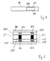
- FIG. 4 is the cross section along the line A-B the credit card 10 shown in FIG. 1.
- FIG. 5 is the layered structure of the Chamber with a multilayer floor 90 or one multilayer cover 130 shown.
- the bottom 90 of the Chamber includes a conductive layer 100 that is flush with the bottom of the credit card 10 completes.
- the Conductive layer 100 is intended to prevent charges from Friction of the credit card 10 on plastic towels and Similar are applied from the outside and thereby the Can influence the display.
- an insulating layer 110 is applied, which in turn by one corresponding to information to be displayed electrostatically chargeable layer 120 is covered.
- the Chamber is closed by a cover 130, the one includes highly conductive layer 140 which is aligned with the top of the Credit card 10 is preferably flush.
- the Cover 130 is constructed similarly to floor 90. With in other words, conductive layer 140 is followed by one Insulating layer 150, on which in turn an electrostatic chargeable layer 160 is applied.
- the electrostatic chargeable layer 160 is transparent.
- the facing each other inside the chamber form electrostatically chargeable layers 160 and 120 a cavity partially with an electrostatic rechargeable powder 105 is filled.
- On the cavity delimiting surfaces of the electrostatically chargeable Layers 120 and 160 are each an insulating layer 155 upset.
- the credit to be displayed is in the form of Loads 122, 124, 162 and 164 on the two electrostatically chargeable layers 120 and 160 such applied that the color powder 105 between the floor 90 and the cover 130 on the electrostatically charged Layers 120 and 160 in the form of those to be represented Information accumulates.
- the charges are, for example, in the reader of a card phone by a Electrode grid applied capacitively. To the card phone erasers / writers, Vending machines etc. should be designed accordingly.
- FIG. 6 is a schematic of a prepaid card shown, the optical display device 20 and has a memory 170.
- the memory can for example from a card phone with the current one Card 110 credit can be loaded.
- the memory 170 is with the optical display device 20, for example a liquid crystal display.
- the credit card has an integrated feed circuit 180 on that a solar cell array 190 and an associated Capacitor 200 includes.
- the capacitor 200 is on the Solar cell field 190 is charged and used Power supply to the memory 170 and / or the Liquid crystal display 20.
- Fig. 7 is a credit card, which in turn one Memory 170 and an optical display device 20, for example, a liquid crystal display.
- the Credit card has a feed circuit 180, the an energy store 200 in the form of a capacitor and has one or more induction loops 210.
- the Capacitor 200 is charged by the prepaid card for example in a reader / writer Card phones is used, which also has a Induction loop.
- the capacitor 200 will then via an inductive coupling between the induction loop 210 and the induction loop in the card phone charged while the card is in the reader located. In this way, contactless charging of the Capacitor 200 possible.
- the capacitor 200 should be one have sufficient capacity for the memory 170 and also the liquid crystal display over a longer one Can be supplied with energy for a period of time.
Landscapes
- Engineering & Computer Science (AREA)
- Physics & Mathematics (AREA)
- General Physics & Mathematics (AREA)
- Theoretical Computer Science (AREA)
- Computer Hardware Design (AREA)
- Microelectronics & Electronic Packaging (AREA)
- Credit Cards Or The Like (AREA)
- Information Retrieval, Db Structures And Fs Structures Therefor (AREA)
Applications Claiming Priority (2)
| Application Number | Priority Date | Filing Date | Title |
|---|---|---|---|
| DE19645869 | 1996-11-07 | ||
| DE19645869A DE19645869A1 (de) | 1996-11-07 | 1996-11-07 | Tragbarer, kartenförmiger Datenträger mit einer optischen Anzeigeeinrichtung |
Publications (3)
| Publication Number | Publication Date |
|---|---|
| EP0841633A2 true EP0841633A2 (fr) | 1998-05-13 |
| EP0841633A3 EP0841633A3 (fr) | 2000-07-12 |
| EP0841633B1 EP0841633B1 (fr) | 2005-08-10 |
Family
ID=7810892
Family Applications (1)
| Application Number | Title | Priority Date | Filing Date |
|---|---|---|---|
| EP97118387A Expired - Lifetime EP0841633B1 (fr) | 1996-11-07 | 1997-10-23 | Porteur d'informations portable sous la forme d'une carte avec un dispositif d'affichage optique |
Country Status (3)
| Country | Link |
|---|---|
| EP (1) | EP0841633B1 (fr) |
| AT (1) | ATE301851T1 (fr) |
| DE (2) | DE19645869A1 (fr) |
Cited By (1)
| Publication number | Priority date | Publication date | Assignee | Title |
|---|---|---|---|---|
| DE10132893A1 (de) * | 2001-07-06 | 2003-01-16 | Giesecke & Devrient Gmbh | Verfahren zum Einbau eines Displayelements |
Families Citing this family (3)
| Publication number | Priority date | Publication date | Assignee | Title |
|---|---|---|---|---|
| DE10119944A1 (de) * | 2001-04-24 | 2002-10-31 | Giesecke & Devrient Gmbh | Datenträgerkarte |
| DE10248386B4 (de) * | 2002-10-17 | 2006-08-31 | Giesecke & Devrient Gmbh | Tragbarer elektronischer Datenträger mit integriertem Display |
| US10919729B2 (en) * | 2014-11-17 | 2021-02-16 | Halliburton Energy Services, Inc. | Self-retractable coiled electrical cable |
Family Cites Families (14)
| Publication number | Priority date | Publication date | Assignee | Title |
|---|---|---|---|---|
| US3792308A (en) * | 1970-06-08 | 1974-02-12 | Matsushita Electric Industrial Co Ltd | Electrophoretic display device of the luminescent type |
| US4442019A (en) * | 1978-05-26 | 1984-04-10 | Marks Alvin M | Electroordered dipole suspension |
| JPS5911479A (ja) * | 1982-07-10 | 1984-01-21 | Nippon Telegr & Teleph Corp <Ntt> | 表示部を有するカ−ドの給電機構 |
| JPS60220475A (ja) * | 1984-04-17 | 1985-11-05 | Nippon Signal Co Ltd:The | 磁気カ−ド処理装置 |
| GB8509135D0 (en) * | 1985-04-10 | 1985-05-15 | Gen Electric Co Plc | Transaction system |
| JPS61273786A (ja) * | 1985-05-29 | 1986-12-04 | Pilot Pen Co Ltd:The | 可視磁気カ−ド |
| JPS629470A (ja) * | 1985-07-05 | 1987-01-17 | Casio Comput Co Ltd | 個人証明カ−ドにおける本人照合方式 |
| JPH01116786A (ja) * | 1987-10-30 | 1989-05-09 | Hitachi Ltd | 表示機能付きカード |
| JPH02165311A (ja) * | 1988-12-20 | 1990-06-26 | Murata Mfg Co Ltd | Icカード |
| JPH0375686A (ja) * | 1989-08-17 | 1991-03-29 | Alps Electric Co Ltd | エレクトロルミネッセンス素子 |
| DE4107311C2 (de) * | 1991-03-07 | 1996-02-08 | Telefunken Microelectron | Verfahren zur drahtlosen Übertragung von Daten auf einen Datenträger |
| DE4138131A1 (de) * | 1991-10-19 | 1993-04-22 | Provera Ges Fuer Projektierung | Kontaktlose chip-karte mit integriertem mikroprozessor und vorrichtung zum lesen und eingeben von informationen |
| JPH08115399A (ja) * | 1994-10-19 | 1996-05-07 | Toshiba Corp | メモリカード |
| JPH08118854A (ja) * | 1994-10-19 | 1996-05-14 | Dainippon Printing Co Ltd | 磁気カード |
-
1996
- 1996-11-07 DE DE19645869A patent/DE19645869A1/de not_active Ceased
-
1997
- 1997-10-23 EP EP97118387A patent/EP0841633B1/fr not_active Expired - Lifetime
- 1997-10-23 DE DE59712386T patent/DE59712386D1/de not_active Expired - Lifetime
- 1997-10-23 AT AT97118387T patent/ATE301851T1/de active
Cited By (2)
| Publication number | Priority date | Publication date | Assignee | Title |
|---|---|---|---|---|
| DE10132893A1 (de) * | 2001-07-06 | 2003-01-16 | Giesecke & Devrient Gmbh | Verfahren zum Einbau eines Displayelements |
| DE10132893B4 (de) * | 2001-07-06 | 2014-02-27 | Giesecke & Devrient Gmbh | Verfahren zum Einbau eines Displayelements |
Also Published As
| Publication number | Publication date |
|---|---|
| EP0841633A3 (fr) | 2000-07-12 |
| DE19645869A1 (de) | 1998-05-14 |
| DE59712386D1 (de) | 2005-09-15 |
| ATE301851T1 (de) | 2005-08-15 |
| EP0841633B1 (fr) | 2005-08-10 |
Similar Documents
| Publication | Publication Date | Title |
|---|---|---|
| DE3687186T2 (de) | Transaktionskarte. | |
| EP0385290B1 (fr) | Dispositif et méthode pour simplifier l'utilisation d'un ensemble de cartes de crédit et similaires | |
| DE2840325C2 (fr) | ||
| EP2323085A1 (fr) | Système de billetterie | |
| EP0486960A2 (fr) | Dispositif pour l'activation codée d'une carte de circuit | |
| EP0268106A2 (fr) | Système pour effectuer des transactions sans argent liquide | |
| EP0617818A1 (fr) | Support de donnees. | |
| DE19737565A1 (de) | Chipkarte, bestehend aus einem Kartenkörper, mit wenigstens einem elektronischen Chip, Kontaktfeld mit Kontakten und/oder Spulen | |
| DE3111516C2 (fr) | ||
| EP0823104B1 (fr) | Cartes electroniques de credit et procede de rechargement de cartes electroniques de credit | |
| EP0841633A2 (fr) | Porteur d'informations portable sous la forme d'une carte avec un dispositif d'affichage optique | |
| DE19740893A1 (de) | Chipkarte mit elektronisch aktiven Logos | |
| DE2659639A1 (de) | Identifizierungskarte mit optisch wiedergewinnbarer in dreidimensionaler form gespeicherter information | |
| DE3636703A1 (de) | Tragbare elektronische vorrichtung | |
| DE4218923A1 (de) | Wertkarte mit elektronik-wert-chip | |
| CH664635A5 (en) | Pencil-shaped cassette for cash-less payment - has optically-readable markings representing amounts of money on moving tape | |
| DE68904782T2 (de) | Tragbare einrichtung zum abfragen, lesen und aufzeichnen einer ic- und/oder einer magnetkarte. | |
| DE19719275C2 (de) | System mit einem tragbaren Terminal und damit verbindbaren Datenträgern | |
| DE4003792A1 (de) | Tragbarer datentraeger mit einem optischen anzeigebereich | |
| DE19939956A1 (de) | Vorrichtung zum Datenaustausch zwischen einer Schreib-/Leseeinrichtung für kontaktbehaftete Chipkarten und einem kontaktlosen Datenträger | |
| EP0405054A1 (fr) | Support de données portatif avec zone de visualisation | |
| DE4205615A1 (de) | Verfahren und einrichtung insbesondere zur eingabe von geheimen identifizierungsdaten in elektronische datensysteme | |
| DE19544144A1 (de) | Verfahren zur Datenübertragung zwischen Datenträgerkarten | |
| EP2431924B1 (fr) | Support de données portatif doté d'un détecteur de flux comme élément d'affichage | |
| DE10002837C2 (de) | Vorrichtung zum Bearbeiten von Datenträgerkarten |
Legal Events
| Date | Code | Title | Description |
|---|---|---|---|
| PUAI | Public reference made under article 153(3) epc to a published international application that has entered the european phase |
Free format text: ORIGINAL CODE: 0009012 |
|
| AK | Designated contracting states |
Kind code of ref document: A2 Designated state(s): AT BE CH DE DK ES FI FR GB GR IE IT LI LU MC NL PT SE |
|
| RIC1 | Information provided on ipc code assigned before grant |
Free format text: 7G 06K 19/077 A, 7G 06K 1/12 B, 7G 06K 19/06 B, 7G 06K 19/04 B |
|
| PUAL | Search report despatched |
Free format text: ORIGINAL CODE: 0009013 |
|
| AK | Designated contracting states |
Kind code of ref document: A3 Designated state(s): AT BE CH DE DK ES FI FR GB GR IE IT LI LU MC NL PT SE |
|
| 17P | Request for examination filed |
Effective date: 20010112 |
|
| AKX | Designation fees paid |
Free format text: AT BE CH DE DK ES FI FR GB GR IE IT LI LU MC NL PT SE |
|
| 17Q | First examination report despatched |
Effective date: 20030703 |
|
| RIC1 | Information provided on ipc code assigned before grant |
Ipc: 7G 06K 19/04 B Ipc: 7G 06K 19/06 B Ipc: 7G 06K 1/12 A |
|
| GRAP | Despatch of communication of intention to grant a patent |
Free format text: ORIGINAL CODE: EPIDOSNIGR1 |
|
| GRAA | (expected) grant |
Free format text: ORIGINAL CODE: 0009210 |
|
| GRAS | Grant fee paid |
Free format text: ORIGINAL CODE: EPIDOSNIGR3 |
|
| AK | Designated contracting states |
Kind code of ref document: B1 Designated state(s): AT BE CH DE DK ES FI FR GB GR IE IT LI LU MC NL PT SE |
|
| PG25 | Lapsed in a contracting state [announced via postgrant information from national office to epo] |
Ref country code: NL Free format text: LAPSE BECAUSE OF FAILURE TO SUBMIT A TRANSLATION OF THE DESCRIPTION OR TO PAY THE FEE WITHIN THE PRESCRIBED TIME-LIMIT Effective date: 20050810 Ref country code: IT Free format text: LAPSE BECAUSE OF FAILURE TO SUBMIT A TRANSLATION OF THE DESCRIPTION OR TO PAY THE FEE WITHIN THE PRESCRIBED TIME-LIMIT;WARNING: LAPSES OF ITALIAN PATENTS WITH EFFECTIVE DATE BEFORE 2007 MAY HAVE OCCURRED AT ANY TIME BEFORE 2007. THE CORRECT EFFECTIVE DATE MAY BE DIFFERENT FROM THE ONE RECORDED. Effective date: 20050810 Ref country code: IE Free format text: LAPSE BECAUSE OF FAILURE TO SUBMIT A TRANSLATION OF THE DESCRIPTION OR TO PAY THE FEE WITHIN THE PRESCRIBED TIME-LIMIT Effective date: 20050810 Ref country code: FI Free format text: LAPSE BECAUSE OF FAILURE TO SUBMIT A TRANSLATION OF THE DESCRIPTION OR TO PAY THE FEE WITHIN THE PRESCRIBED TIME-LIMIT Effective date: 20050810 Ref country code: ES Free format text: LAPSE BECAUSE OF FAILURE TO SUBMIT A TRANSLATION OF THE DESCRIPTION OR TO PAY THE FEE WITHIN THE PRESCRIBED TIME-LIMIT Effective date: 20050810 |
|
| REG | Reference to a national code |
Ref country code: GB Ref legal event code: FG4D Free format text: NOT ENGLISH |
|
| REG | Reference to a national code |
Ref country code: CH Ref legal event code: EP |
|
| REG | Reference to a national code |
Ref country code: CH Ref legal event code: NV Representative=s name: ISLER & PEDRAZZINI AG |
|
| REG | Reference to a national code |
Ref country code: IE Ref legal event code: FG4D Free format text: LANGUAGE OF EP DOCUMENT: GERMAN |
|
| REF | Corresponds to: |
Ref document number: 59712386 Country of ref document: DE Date of ref document: 20050915 Kind code of ref document: P |
|
| PG25 | Lapsed in a contracting state [announced via postgrant information from national office to epo] |
Ref country code: MC Free format text: LAPSE BECAUSE OF NON-PAYMENT OF DUE FEES Effective date: 20051031 Ref country code: LU Free format text: LAPSE BECAUSE OF NON-PAYMENT OF DUE FEES Effective date: 20051031 Ref country code: BE Free format text: LAPSE BECAUSE OF NON-PAYMENT OF DUE FEES Effective date: 20051031 |
|
| PG25 | Lapsed in a contracting state [announced via postgrant information from national office to epo] |
Ref country code: SE Free format text: LAPSE BECAUSE OF FAILURE TO SUBMIT A TRANSLATION OF THE DESCRIPTION OR TO PAY THE FEE WITHIN THE PRESCRIBED TIME-LIMIT Effective date: 20051110 Ref country code: GR Free format text: LAPSE BECAUSE OF FAILURE TO SUBMIT A TRANSLATION OF THE DESCRIPTION OR TO PAY THE FEE WITHIN THE PRESCRIBED TIME-LIMIT Effective date: 20051110 Ref country code: DK Free format text: LAPSE BECAUSE OF FAILURE TO SUBMIT A TRANSLATION OF THE DESCRIPTION OR TO PAY THE FEE WITHIN THE PRESCRIBED TIME-LIMIT Effective date: 20051110 |
|
| GBT | Gb: translation of ep patent filed (gb section 77(6)(a)/1977) |
Effective date: 20051102 |
|
| PG25 | Lapsed in a contracting state [announced via postgrant information from national office to epo] |
Ref country code: PT Free format text: LAPSE BECAUSE OF FAILURE TO SUBMIT A TRANSLATION OF THE DESCRIPTION OR TO PAY THE FEE WITHIN THE PRESCRIBED TIME-LIMIT Effective date: 20060110 |
|
| NLV1 | Nl: lapsed or annulled due to failure to fulfill the requirements of art. 29p and 29m of the patents act | ||
| REG | Reference to a national code |
Ref country code: IE Ref legal event code: FD4D |
|
| ET | Fr: translation filed | ||
| PLBE | No opposition filed within time limit |
Free format text: ORIGINAL CODE: 0009261 |
|
| STAA | Information on the status of an ep patent application or granted ep patent |
Free format text: STATUS: NO OPPOSITION FILED WITHIN TIME LIMIT |
|
| 26N | No opposition filed |
Effective date: 20060511 |
|
| REG | Reference to a national code |
Ref country code: CH Ref legal event code: PCAR Free format text: ISLER & PEDRAZZINI AG;POSTFACH 1772;8027 ZUERICH (CH) |
|
| BERE | Be: lapsed |
Owner name: DEUTSCHE TELEKOM A.G. Effective date: 20051031 |
|
| REG | Reference to a national code |
Ref country code: FR Ref legal event code: PLFP Year of fee payment: 19 |
|
| PGFP | Annual fee paid to national office [announced via postgrant information from national office to epo] |
Ref country code: DE Payment date: 20151022 Year of fee payment: 19 Ref country code: GB Payment date: 20151026 Year of fee payment: 19 Ref country code: CH Payment date: 20151026 Year of fee payment: 19 |
|
| PGFP | Annual fee paid to national office [announced via postgrant information from national office to epo] |
Ref country code: AT Payment date: 20151022 Year of fee payment: 19 Ref country code: FR Payment date: 20151026 Year of fee payment: 19 |
|
| REG | Reference to a national code |
Ref country code: DE Ref legal event code: R119 Ref document number: 59712386 Country of ref document: DE |
|
| REG | Reference to a national code |
Ref country code: CH Ref legal event code: PL |
|
| REG | Reference to a national code |
Ref country code: AT Ref legal event code: MM01 Ref document number: 301851 Country of ref document: AT Kind code of ref document: T Effective date: 20161023 |
|
| GBPC | Gb: european patent ceased through non-payment of renewal fee |
Effective date: 20161023 |
|
| REG | Reference to a national code |
Ref country code: FR Ref legal event code: ST Effective date: 20170630 |
|
| PG25 | Lapsed in a contracting state [announced via postgrant information from national office to epo] |
Ref country code: DE Free format text: LAPSE BECAUSE OF NON-PAYMENT OF DUE FEES Effective date: 20170503 Ref country code: FR Free format text: LAPSE BECAUSE OF NON-PAYMENT OF DUE FEES Effective date: 20161102 Ref country code: CH Free format text: LAPSE BECAUSE OF NON-PAYMENT OF DUE FEES Effective date: 20161031 Ref country code: LI Free format text: LAPSE BECAUSE OF NON-PAYMENT OF DUE FEES Effective date: 20161031 Ref country code: GB Free format text: LAPSE BECAUSE OF NON-PAYMENT OF DUE FEES Effective date: 20161023 |
|
| PG25 | Lapsed in a contracting state [announced via postgrant information from national office to epo] |
Ref country code: AT Free format text: LAPSE BECAUSE OF NON-PAYMENT OF DUE FEES Effective date: 20161023 |