EP0841704A1 - Transistorhalbleiterbauelement und Verfahren zu dessen Herstellung - Google Patents
Transistorhalbleiterbauelement und Verfahren zu dessen Herstellung Download PDFInfo
- Publication number
- EP0841704A1 EP0841704A1 EP97113111A EP97113111A EP0841704A1 EP 0841704 A1 EP0841704 A1 EP 0841704A1 EP 97113111 A EP97113111 A EP 97113111A EP 97113111 A EP97113111 A EP 97113111A EP 0841704 A1 EP0841704 A1 EP 0841704A1
- Authority
- EP
- European Patent Office
- Prior art keywords
- quantum well
- well layer
- layer
- accordance
- quantum
- Prior art date
- Legal status (The legal status is an assumption and is not a legal conclusion. Google has not performed a legal analysis and makes no representation as to the accuracy of the status listed.)
- Withdrawn
Links
Images




Classifications
-
- B—PERFORMING OPERATIONS; TRANSPORTING
- B82—NANOTECHNOLOGY
- B82Y—SPECIFIC USES OR APPLICATIONS OF NANOSTRUCTURES; MEASUREMENT OR ANALYSIS OF NANOSTRUCTURES; MANUFACTURE OR TREATMENT OF NANOSTRUCTURES
- B82Y10/00—Nanotechnology for information processing, storage or transmission, e.g. quantum computing or single electron logic
-
- H—ELECTRICITY
- H10—SEMICONDUCTOR DEVICES; ELECTRIC SOLID-STATE DEVICES NOT OTHERWISE PROVIDED FOR
- H10D—INORGANIC ELECTRIC SEMICONDUCTOR DEVICES
- H10D30/00—Field-effect transistors [FET]
- H10D30/01—Manufacture or treatment
- H10D30/014—Manufacture or treatment of FETs having zero-dimensional [0D] or one-dimensional [1D] channels, e.g. quantum wire FETs, single-electron transistors [SET] or Coulomb blockade transistors
-
- H—ELECTRICITY
- H10—SEMICONDUCTOR DEVICES; ELECTRIC SOLID-STATE DEVICES NOT OTHERWISE PROVIDED FOR
- H10D—INORGANIC ELECTRIC SEMICONDUCTOR DEVICES
- H10D30/00—Field-effect transistors [FET]
- H10D30/01—Manufacture or treatment
- H10D30/015—Manufacture or treatment of FETs having heterojunction interface channels or heterojunction gate electrodes, e.g. HEMT
-
- H—ELECTRICITY
- H10—SEMICONDUCTOR DEVICES; ELECTRIC SOLID-STATE DEVICES NOT OTHERWISE PROVIDED FOR
- H10D—INORGANIC ELECTRIC SEMICONDUCTOR DEVICES
- H10D30/00—Field-effect transistors [FET]
- H10D30/40—FETs having zero-dimensional [0D], one-dimensional [1D] or two-dimensional [2D] charge carrier gas channels
- H10D30/43—FETs having zero-dimensional [0D], one-dimensional [1D] or two-dimensional [2D] charge carrier gas channels having one-dimensional [1D] charge carrier gas channels, e.g. quantum wire FETs or transistors having 1D quantum-confined channels
-
- H—ELECTRICITY
- H10—SEMICONDUCTOR DEVICES; ELECTRIC SOLID-STATE DEVICES NOT OTHERWISE PROVIDED FOR
- H10D—INORGANIC ELECTRIC SEMICONDUCTOR DEVICES
- H10D30/00—Field-effect transistors [FET]
- H10D30/40—FETs having zero-dimensional [0D], one-dimensional [1D] or two-dimensional [2D] charge carrier gas channels
- H10D30/47—FETs having zero-dimensional [0D], one-dimensional [1D] or two-dimensional [2D] charge carrier gas channels having two-dimensional [2D] charge carrier gas channels, e.g. nanoribbon FETs or high electron mobility transistors [HEMT]
- H10D30/471—High electron mobility transistors [HEMT] or high hole mobility transistors [HHMT]
- H10D30/473—High electron mobility transistors [HEMT] or high hole mobility transistors [HHMT] having confinement of carriers by multiple heterojunctions, e.g. quantum well HEMT
- H10D30/4732—High electron mobility transistors [HEMT] or high hole mobility transistors [HHMT] having confinement of carriers by multiple heterojunctions, e.g. quantum well HEMT using Group III-V semiconductor material
- H10D30/4738—High electron mobility transistors [HEMT] or high hole mobility transistors [HHMT] having confinement of carriers by multiple heterojunctions, e.g. quantum well HEMT using Group III-V semiconductor material having multiple donor layers
-
- H—ELECTRICITY
- H10—SEMICONDUCTOR DEVICES; ELECTRIC SOLID-STATE DEVICES NOT OTHERWISE PROVIDED FOR
- H10D—INORGANIC ELECTRIC SEMICONDUCTOR DEVICES
- H10D62/00—Semiconductor bodies, or regions thereof, of devices having potential barriers
- H10D62/80—Semiconductor bodies, or regions thereof, of devices having potential barriers characterised by the materials
- H10D62/81—Semiconductor bodies, or regions thereof, of devices having potential barriers characterised by the materials of structures exhibiting quantum-confinement effects, e.g. single quantum wells; of structures having periodic or quasi-periodic potential variation
- H10D62/815—Semiconductor bodies, or regions thereof, of devices having potential barriers characterised by the materials of structures exhibiting quantum-confinement effects, e.g. single quantum wells; of structures having periodic or quasi-periodic potential variation of structures having periodic or quasi-periodic potential variation, e.g. superlattices or multiple quantum wells [MQW]
- H10D62/8161—Semiconductor bodies, or regions thereof, of devices having potential barriers characterised by the materials of structures exhibiting quantum-confinement effects, e.g. single quantum wells; of structures having periodic or quasi-periodic potential variation of structures having periodic or quasi-periodic potential variation, e.g. superlattices or multiple quantum wells [MQW] potential variation due to variations in composition or crystallinity, e.g. heterojunction superlattices
- H10D62/8162—Semiconductor bodies, or regions thereof, of devices having potential barriers characterised by the materials of structures exhibiting quantum-confinement effects, e.g. single quantum wells; of structures having periodic or quasi-periodic potential variation of structures having periodic or quasi-periodic potential variation, e.g. superlattices or multiple quantum wells [MQW] potential variation due to variations in composition or crystallinity, e.g. heterojunction superlattices having quantum effects only in the vertical direction, i.e. layered structures having quantum effects solely resulting from vertical potential variation
- H10D62/8164—Semiconductor bodies, or regions thereof, of devices having potential barriers characterised by the materials of structures exhibiting quantum-confinement effects, e.g. single quantum wells; of structures having periodic or quasi-periodic potential variation of structures having periodic or quasi-periodic potential variation, e.g. superlattices or multiple quantum wells [MQW] potential variation due to variations in composition or crystallinity, e.g. heterojunction superlattices having quantum effects only in the vertical direction, i.e. layered structures having quantum effects solely resulting from vertical potential variation comprising only semiconductor materials
-
- H—ELECTRICITY
- H10—SEMICONDUCTOR DEVICES; ELECTRIC SOLID-STATE DEVICES NOT OTHERWISE PROVIDED FOR
- H10D—INORGANIC ELECTRIC SEMICONDUCTOR DEVICES
- H10D62/00—Semiconductor bodies, or regions thereof, of devices having potential barriers
- H10D62/60—Impurity distributions or concentrations
- H10D62/605—Planar doped, e.g. atomic-plane doped or delta-doped
-
- H—ELECTRICITY
- H10—SEMICONDUCTOR DEVICES; ELECTRIC SOLID-STATE DEVICES NOT OTHERWISE PROVIDED FOR
- H10D—INORGANIC ELECTRIC SEMICONDUCTOR DEVICES
- H10D62/00—Semiconductor bodies, or regions thereof, of devices having potential barriers
- H10D62/80—Semiconductor bodies, or regions thereof, of devices having potential barriers characterised by the materials
- H10D62/85—Semiconductor bodies, or regions thereof, of devices having potential barriers characterised by the materials being Group III-V materials, e.g. GaAs
- H10D62/8503—Nitride Group III-V materials, e.g. AlN or GaN
Definitions
- the present invention relates to a method of manufacturing a semiconductor transistor device on a substrate, the device comprising source and drain contacts to a conductive layer extending between the contacts and at least one gate electrode disposed adjacent to and spaced from the conductive layer. Furthermore, the present invention relates to a semiconductor transistor device.
- the FET is provided with a superlattice structure comprising alternating layers of two materials having different band gaps and a ⁇ doped layer is provided in each of the layers of smaller band gap.
- US patents 5,396,089 and 5,338,692 which correspond to the European application with the publication number EP-A-394 757, disclose a novel and extremely interesting design for FETs using so-called in-plane gates. More specifically, a semiconductor substrate having a two-dimensional conductive layer formed by a two-dimensional electron gas is divided up to form lateral potential boundaries defining source, drain and gate regions. That is to say, the gate is formed by a portion of the two-dimensional electron gas itself, which is insulated from a conductive channel formed from the two-dimensional electron gas forming and extending between the source and drain regions.
- the lateral potential boundaries insulating the gate from the conductive channel and separating the source from the drain can be formed by a number of different methods, for example by ion implantation. Alternatively, it can be formed by etching trenches into the substrate as is described in US patent 5,385,865 and in the corresponding European application with the publication number EP-A-464 834.
- High barriers allow for large 2DEG concentrations n .
- the devices can operate at higher temperatures.
- the possibilities to increase the conductivity by simply increasing the dopant density are limited for several reasons.
- Al,GaAs system high electron mobilities of several 100 m 2 /Vs at low temperatures have been reported.
- the systems consist of multi-quantum wells with low carrier densities of 0.64 x 10 15 m -2 per quantum well (see, for example, the above named paper by L.N. Pfeiffer, K.W. West, J.P. Eisenstein, K.W. Baldwin and P. Gammel, Appl. Phys. Lett.
- HEMTs high electron mobility transistors
- single electron transistors there is still a need to increase the electron density while retaining the high electron mobility, for example to provide a steeper current gain characteristic in FETs and a steeper charge distribution profile at the boundaries of low-dimensional structures, i.e. quantum wire or quantum dot structures and thus a higher separation of the quantized energy levels in order to reduce intersubband scattering.
- a method of the initially named kind which is characterized by the step of growing in sequence on said substrate a first superlattice, a quantum well layer and a second superlattice, said first and second superlattices forming the barriers for the quantum well layer, and by the further step of ⁇ doping each of said first and second superlattices to form at least one ⁇ doped layer therein, whereby to enhance the conductivity of the electrons in the quantum well layer.
- the semiconductor transistor device formed by this method is thus characterized by an active region formed on the substrate and comprising in sequence a first superlattice, a quantum well layer and a second superlattice, said first and second superlattices forming the barriers for the quantum well layer and by at least one ⁇ doped layer in each of said first and second superlattices.
- This method and device represent a new concept for the enhancement of both the carrier concentration and the reduction of remote impurity scattering (RIS) in single quantum wells (SQW), thereby significantly increasing the conductivity.
- RIS remote impurity scattering
- impurity scattering in remotely doped single quantum wells can be effectively reduced by the presence of heavy mass X-electrons in the short period superlattices in the direct vicinity of the dopant atoms in the barriers formed by the short period superlattices.
- These X-electrons exhibit an extremely high screening capability and are able to smooth the potential fluctuations caused by the random distribution of the dopants. They are strongly localized and do not contribute to the conductivity. In this way it has proved possible to increase the mobility by reducing the impurity scattering and to do so without reducing the electron density in the quantum well layer.
- each of the first and second superlattices consist of different elements or compounds, thereby increasing the barrier height and therefore the electron density in the quantum well.
- the superlattices could consist of alternate layers of AlAs/GaAs, or GaN/AlGaN or GaN/SiC, or Ge/Si. They should not, however, consist of mixed crystals such as Al x Ga 1-x As/GaS/GaS or Ge x Si 1-x /Si because with such mixed crystals the electrons are not localized in the quantum wells but rather distributed within the crystal.
- the thickness of the barrier layers of the superlattice structures are preferably selected so that the electrons from the donors in the ⁇ doped layers are localized in the neighboring barrier layers. This screens the fluctuations of the potential from the charge donors and other impurities or surface charges, thus reducing the scattering and in particular the ionized impurity scattering and therefore increases the mobility of the electrons in the quantum well layer.
- the active region of the semiconductor device comprising the first and second superlattices and the quantum well layer are preferably made in a III-V or IV-IV material system, in particular in AlAs/GaAs or Ge/Si or GaN/AlGaN or GaN/SiC.
- the quantum well layer can, however, advantageously comprise a mixed crystal. This makes it possible to depress the energy level of the quantum well and to thereby increase the quantum well density (i.e. the density of electrons in the quantum well).
- the quantum well density i.e. the density of electrons in the quantum well.
- In can be added to the GaAs quantum well to make an InGaAs mixed crystal.
- the active region of the transistor device can also be realized with advantage as a quantum dot or quantum wire structure. This leads to improved sharpness of the lateral profile of the electron distribution while retaining the high mobility.
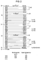
- Fig. 1 there is shown a schematic diagram of a semiconductor structure in accordance with the present invention. It is emphasized that the diagram is not to scale and more specifically the relative sizes of the layers illustrated in the diagram of Fig. 1 do not accurately reflect the relative sizes of the layers of the actual structure, which will be later described in more detail.
- Fig. 1 shows a semiconductor structure 10 comprising a semi-insulating substrate 12, for example of gallium arsenide.
- a buffer layer 16 for example consisting of 500 nm of gallium arsenide, in order to prevent impurities and defects migrating from the substrate through to the overlying structure, and to ensure a sound crystallographic structure.
- a first superlattice system 20 consisting, in this example, of alternating layers of gallium arsenide and aluminum arsenide, for example with a total of sixty-three periods. These layers are essentially undoped, however, one of the gallium arsenide layers, i.e.
- the layer of the material with the lower band gap is provided with a ⁇ doped layer 22, i.e. a single doped monolayer.
- the dopant is silicon and the doping density is 2 x 10 12 cm -2 . It has been found beneficial if this ⁇ doped layer is then followed by a further three and a half periods of the superlattice of alternating composition.
- this first superlattice structure there is then grown a single quantum well layer 24 and the quantum well layer 24 is grown in the material having the smaller band gap, i.e. in this example in gallium arsenide.
- the well layer 24 is undoped
- a second superlattice structure 26 again comprising two layers of different materials, and indeed the same materials that are used for the alternating layers of the superlattice of the first superlattice structure 20.
- one of the layers of the material having the lower band gap is subjected to ⁇ doping to produce a second ⁇ doped layer 28.
- ⁇ doping to produce a second ⁇ doped layer 28.
- the quantum well layer 24 and the second ⁇ doped layer 28 there are preferably again provided three and a half periods of alternating composition.
- the total number of periods of the second superlattice structure is also sixty-three.
- top layer 32 of the same material as the substrate but doped at a relatively high level to provide a layer of high conductivity.
- the top layer 32 comprises GaAs and is doped with silicon with a doping density of 1.5 x 10 18 cm -3 .
- an etch stop layer 30 e.g. of Al 0.23 Ga 0.77 As between the second superlattice structure 26 and the top layer 32.
- the first and second superlattice structures will generally always be formed by alternating layers consisting of different elements or of different compounds, for example, without restrictions, AlAs/GaAs, or Ge/Si or GaN/AlGaN or GaN/SiC. They will ordinarily not be mixed crystal layers, i.e. for example not Al x Ga 1-x As or Ge x Si 1-x .
- the single quantum well layer 24 can, however, consist of a mixed crystal material, for example InGaAs.
- the total number of periods of the first and second superlattices i.e. the total number of pairs of alternating layers, is not critical but would typically be of the order of 50 layers or so.
- the thickness selected for the individual layers of the superlattice structures are those typical for such structures.
- the precise position of the ⁇ doped layers 22 and 28 in the first and second superlattices 20 and 26 is also not critical. However, favorable results have been obtained if two or three periods of the superlattice are disposed between each ⁇ doped layer 22, 28 and the single quantum well layer 24.
- the region comprising the first and second superlattices 20, 26 with the ⁇ doped layers 22 and 28 and the single quantum well layer 24 disposed between them will generally be referred to as the active region of the semiconductor structure.
- This active region is designated generally by the reference numeral 34.
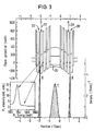
- Fig. 3 shows the band structure for the active region 34 and is in fact a composite drawing showing both the band structure and the charge distribution of the electrons.
- the band diagram shows at the center the quantum well 24' formed by the single quantum well layer 24 in the structure of Fig. 1.
- the barriers 20' and 26' formed by the first and second superlattices 20 and 26 of Fig. 1.
- the band diagram does not show all the periods of the first and second superlattices but rather only the last five and indeed it would be possible to restrict the total number of periods of the superlattices.
- the letter ⁇ shows the position of the ⁇ doped layers 22 and 28 of the structure of Fig.
- each ⁇ doped layer 22, 28 and the quantum well 24' of the single quantum well layer 24 there are three and a half periods of the superlattice structure disposed between each ⁇ doped layer 22, 28 and the quantum well 24' of the single quantum well layer 24. It will also be noted from the position of the arrows associated with the deltas that the position of each ⁇ doped layer is disposed in the middle of the - otherwise undoped - material having the lower band gap, i.e. in the GaAs in the AlAs/GaAs system.
- the dopant atoms (silicon in this example) used for the ⁇ doping are localized in the middle of the respective layers, the electrons provided by these dopant atoms transfer into two energy levels in the two neighboring layers having the higher band gap. These two energy levels are illustrated by thin horizontal lines in Fig. 3 and the electron concentrations in these levels are indicated by the PL intensity plot shown in the inset square graph in the bottom left hand corner of Fig. 3.
- the single quantum well 24' has two spaced apart energy levels - again shown by horizontal lines - of which only the lower energy level is normally occupied by electrons.
- the X-electrons resulting from the dopants are localized and uniformly distributed in the quantized energy levels at the minima of the fluctuating potentials caused by the randomly distributed dopants.
- the X-electrons thus screen the electrons in the single quantum well 24' from the fluctuating potential caused by the randomly distributed dopants. It is this that is believed to enhance the mobility of the electrons in the quantum well 24' without disadvantageously affecting the electron density.
- FIG. 4 there is shown a first example of an FET formed using the semiconductor structure 10 of Fig. 1.
- the substrate is provided with source and drain electrodes 36 and 38 respectively which extend through the semiconductor structure 10 and thus provide contacts to the active region 34 in particular.
- a single gate electrode 40 Disposed between the source and drain electrodes 36 and 38 is a single gate electrode 40 which is spaced from the source and drain electrodes 36 and 38 and overlies the 2DEG provided in the quantum well layer 24.
- the top gate 40 is achieved by etching away a central strip portion of the top layer 32 (down to the etch stop layer 30) and by depositing a metallic gate layer on top of the etch stop layer 30.
- These windows can, for example, be produced by ion beam etching.
- Fig. 4 The structure shown in Fig. 4 will immediately be recognized as an FET structure and the conduction between the source and drain electrodes can be controlled via the potential applied to the gate electrode 40.
- Fig. 5 shows a different way of realizing an FET structure on the same substrate.
- the substrate is divided into source 36, drain 38 and gate regions 40 by ion implantation along the lines 46 and 48.
- the structure will be recognized by the person skilled in the art as a typical in-plane gate structure as shown in EP-A-394,757.
- the insulating regions formed by ion implantation along the lines 46 and 48 defining high quality insulating regions, i.e. lateral potential boundaries, which extend perpendicular to the plane of the substrate down through the active region 34.
- Reference numeral 52 denotes the conductive channel of the FET realized in this manner.
- the regions 46 and 48 as trenches by an etching technique as disclosed in EP-A-464 834.
- the trenches so formed could also be filled with an insulator if desired.
- Fig. 6 shows an alternative way of realizing an FET similar to the FET of Fig. 4.
- the gate 40 is not formed as a top gate but as a back gate.
- the same reference numerals are used to denote the same parts or parts having the same function so as to avoid the need to describe each embodiment in great detail.
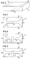
- Fig. 7 shows an alternative starting point for forming an FET using the basic semiconductor structure 10.
- the FET is provided with a conductive channel in the form of a quantum wire 52.
- This quantum wire 52 in fact comprises an elongate section of the 2DEG formed in the substrate 10. This elongate section can be realized in a variety of ways.
- the boundaries 54 and 56 could be realized by ion implantation or etching in the manner described with respect to Fig. 5.
- the regions 58 and 60 could be realized as a split gate arrangement. By controlling the potentials applied to the regions 58 and 60, the regions of the quantum well layer beneath the gates can be depleted of electrons so that only the conductive region 52 remains.
- the semiconductor structure 10 can be etched away in the regions 58 and 60 to a level beneath the active region 34 so that only a narrow web of active region remains, which defines the quantum well wire 52.
- the source and drain regions are contacts to the 2DEG at either end of the quantum wire.
- the gate for controlling the conductivity in the quantum wire 52 can be realized in different ways, as shown in the Figs. 8 and 9.
- the gate 40 is realized as a top gate. This would, for example, be possible if the regions 58 and 60 were removed by etching.
- Fig. 9 the gate 40 is realized as a back gate and this would be possible with all the above explained ways of realizing the structure of Fig. 7.
- the FET has been realized with a single quantum well wire 52, it would also be possible to provide a plurality of quantum well wires connecting the source and drain regions 36 and 38 if desired.
- Fig. 10 now shows a further development of the concept explained with respect to Figs. 7 and 9, in which a quantum dot structure is realized by providing two gates 40 spaced apart along the length of the quantum well wire.
- the quantum dot 62 is defined by the region between the gate electrodes.
- Fig. 11 shows the charge carrier distribution along the conductive channel between the source and drain regions 36 and 38 for the quantum dot structure of Fig. 10.
- Fig. 12 shows two gates 40 which can also be realized as back gates.
- Fig. 13 shows that it may be more convenient to lead the gate connections out to opposite sides of the semiconductor structure 10.
- the gates are both realized as top gates; they could alternatively also be realized as back gates (not shown).
- one gate 40 could be realized as a top gate and one gate 40 as a back gate.
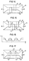
- the invention is not, however, restricted to a single quantum dot. It could, for example, be realized with a plurality of quantum dots (for example with two quantum dots, as shown in Fig. 15). Here one again sees the same basic structure as in Fig. 7, but the structure is now provided with three gate electrodes 40 in order to provide two quantum dots 62.
- the density of charge carriers along the conductive channel is shown schematically in Fig. 16.
- Fig. 17 shows that the three gate electrodes 40 could also be realized as back gates.
- Fig. 19 simply shows an arrangement similar to Fig. 18, but in which the contacts to the two outer gates are led divergently away from each other, which can be beneficial with regard to the very small dimensions of the devices.
- Fig. 20 shows an alternative way of realizing a single dot structure 62, using the split gate arrangement of Fig. 7 as in-plane gates 40.
- the barriers of the GaAs SQW are formed by AlAs/GaAs short-period superlattices (SPSL).
- SPSL short-period superlattices
- the lowest conduction band state can be formed by the X-conduction band state of the AlAs layer, as described by M. Holtz, R. Cingolani, K. Reimann, R. Muralidharan, K. Syassen and K. Ploog, Phys. Rev. B 41 , 3641 (1990)(X-electron).
- the structures under investigation were grown by solid source molecular beam epitaxy on semi-insulating GaAs (001) substrates.
- the barriers consist of a SPSL of 60 periods of 4 monolayer AlAs and 8 monolayer GaAs.
- the carriers in the 10 nm GaAs SQW are provided by remote ⁇ doping with Si at a distance from the SQW interface of 14 nm (sample S1) and 10 nm (sample S2).
- the growth temperature of the lower barrier and the SQW was 580°C, whereas the temperature for the ⁇ doping sheet and its vicinity was 510°C to suppress Si segregation into the well.
- the growth rate and the beam equivalent As 4 -to-Ga pressure ratio were 0.66 ⁇ m/h and 8 respectively.
- the observed (2x4) surface reconstruction during the SPSL and SQW deposition reflects the two-dimensional nucleation growth mode, which was monitored by additional experiments.
- Fig. 21 shows the dependence of the parallel ⁇ xx and transverse ⁇ xy components of the resistivity tensor on the magnetic field.
- the electrons occupy only one subband which is manifested by Shubnikov-de-Haas (SdH) oscillations with only one frequency of the corresponding ⁇ xx component of the conductivity tensor up to the highest gate voltages.
- SdH Shubnikov-de-Haas
- C 2D carries information only from carriers in the high mobility 2DEG.
- the relatively flat region of C at lower gate voltages U g ⁇ -1.5 V corresponds to the depletion of the electrons in the SQW.
- the higher capacitance at U g > -1.5 V and the vanishing of C 2D in the same gate voltage region indicate the presence of additional carriers outside the SQW nearby the doping layer.
- the strong increase of the electron mobility takes place in the same gate voltage region and is, therefore, related to the existence of these carriers.
- Fig. 3 shows the results of model calculations of the potential and charge distribution in the new structure.
- the calculations are performed by the one-dimensional self consistent solution of the Schrödinger and Poisson equations in the effective mass approximation including exchange and correlation interaction energy. These calculations account for two different kinds of electrons.
- These electrons with high mobility are located in the SQW.
- the edge of the higher ⁇ electron subbands in the SQW as well as in the SPSL are more than 170 meV above the Fermi energy. Therefore, they cannot be occupied at low temperatures.
Landscapes
- Engineering & Computer Science (AREA)
- Chemical & Material Sciences (AREA)
- Nanotechnology (AREA)
- Physics & Mathematics (AREA)
- Mathematical Physics (AREA)
- Theoretical Computer Science (AREA)
- Crystallography & Structural Chemistry (AREA)
- Junction Field-Effect Transistors (AREA)
Priority Applications (1)
| Application Number | Priority Date | Filing Date | Title |
|---|---|---|---|
| EP97113111A EP0841704A1 (de) | 1996-11-07 | 1997-07-30 | Transistorhalbleiterbauelement und Verfahren zu dessen Herstellung |
Applications Claiming Priority (3)
| Application Number | Priority Date | Filing Date | Title |
|---|---|---|---|
| EP96117884 | 1996-11-07 | ||
| EP96117884 | 1996-11-07 | ||
| EP97113111A EP0841704A1 (de) | 1996-11-07 | 1997-07-30 | Transistorhalbleiterbauelement und Verfahren zu dessen Herstellung |
Publications (1)
| Publication Number | Publication Date |
|---|---|
| EP0841704A1 true EP0841704A1 (de) | 1998-05-13 |
Family
ID=26142285
Family Applications (1)
| Application Number | Title | Priority Date | Filing Date |
|---|---|---|---|
| EP97113111A Withdrawn EP0841704A1 (de) | 1996-11-07 | 1997-07-30 | Transistorhalbleiterbauelement und Verfahren zu dessen Herstellung |
Country Status (1)
| Country | Link |
|---|---|
| EP (1) | EP0841704A1 (de) |
Cited By (4)
| Publication number | Priority date | Publication date | Assignee | Title |
|---|---|---|---|---|
| WO2001091186A3 (de) * | 2000-05-25 | 2002-05-23 | Rubitec Gesellschaft Fuer Innovation & Technologie Ruhr Univ Bochum Mbh | Halbleiterschichtsystem und verfahren zur herstellung von einem halbleiterschichtsystem mit erhöhter resistenz gegen thermische prozessierung |
| WO2002043156A3 (en) * | 2000-11-21 | 2002-08-29 | Matsushita Electric Industrial Co Ltd | Hemt and communication system using the same |
| WO2003083950A1 (en) | 2002-03-25 | 2003-10-09 | Cree, Inc. | Doped group iii-v nitride materials, and microelectronic devices and device precursor structures comprising same |
| WO2023214872A1 (en) * | 2022-05-06 | 2023-11-09 | Technische Universiteit Delft | Buried-channel semiconductor heterostructures with enhanced band offset |
Citations (4)
| Publication number | Priority date | Publication date | Assignee | Title |
|---|---|---|---|---|
| JPS6235678A (ja) * | 1985-08-09 | 1987-02-16 | Fujitsu Ltd | ダブル・ヘテロ型電界効果トランジスタ |
| JPS62136882A (ja) * | 1985-12-11 | 1987-06-19 | Fujitsu Ltd | 高速電界効果半導体装置 |
| US4882609A (en) * | 1984-11-19 | 1989-11-21 | Max-Planck Gesellschaft Zur Forderung Der Wissenschafter E.V. | Semiconductor devices with at least one monoatomic layer of doping atoms |
| EP0394757A2 (de) * | 1989-04-27 | 1990-10-31 | Max-Planck-Gesellschaft zur Förderung der Wissenschaften e.V. | Verfahren zur Erzeugung von aktiven Halbleiterstrukturen mittels Ausgangsstrukturen mit einer oberflächenparallelen 2D-Ladungsträgerschicht |
-
1997
- 1997-07-30 EP EP97113111A patent/EP0841704A1/de not_active Withdrawn
Patent Citations (4)
| Publication number | Priority date | Publication date | Assignee | Title |
|---|---|---|---|---|
| US4882609A (en) * | 1984-11-19 | 1989-11-21 | Max-Planck Gesellschaft Zur Forderung Der Wissenschafter E.V. | Semiconductor devices with at least one monoatomic layer of doping atoms |
| JPS6235678A (ja) * | 1985-08-09 | 1987-02-16 | Fujitsu Ltd | ダブル・ヘテロ型電界効果トランジスタ |
| JPS62136882A (ja) * | 1985-12-11 | 1987-06-19 | Fujitsu Ltd | 高速電界効果半導体装置 |
| EP0394757A2 (de) * | 1989-04-27 | 1990-10-31 | Max-Planck-Gesellschaft zur Förderung der Wissenschaften e.V. | Verfahren zur Erzeugung von aktiven Halbleiterstrukturen mittels Ausgangsstrukturen mit einer oberflächenparallelen 2D-Ladungsträgerschicht |
Non-Patent Citations (4)
| Title |
|---|
| FRIEDLAND K -J ET AL: "New concept for the reduction of impurity scattering in remotely doped GaAs quantum wells", PHYSICAL REVIEW LETTERS, 25 NOV. 1996, APS, USA, vol. 77, no. 22, ISSN 0031-9007, pages 4616 - 4619, XP002044440 * |
| NGUYEN L D ET AL: "INFLUENCE OF QUANTUM-WELL WIDTH ON DEVICE PERFORMANCE OF AL0.30GA0.70AS/INP0.25GA0.75AS (ON GAAS) MODFET'S", IEEE TRANSACTIONS ON ELECTRON DEVICES, vol. 36, no. 5, 1 May 1989 (1989-05-01), pages 833 - 838, XP000099014 * |
| PATENT ABSTRACTS OF JAPAN vol. 011, no. 217 (E - 523) 14 July 1987 (1987-07-14) * |
| PATENT ABSTRACTS OF JAPAN vol. 011, no. 363 (E - 560) 26 November 1987 (1987-11-26) * |
Cited By (9)
| Publication number | Priority date | Publication date | Assignee | Title |
|---|---|---|---|---|
| WO2001091186A3 (de) * | 2000-05-25 | 2002-05-23 | Rubitec Gesellschaft Fuer Innovation & Technologie Ruhr Univ Bochum Mbh | Halbleiterschichtsystem und verfahren zur herstellung von einem halbleiterschichtsystem mit erhöhter resistenz gegen thermische prozessierung |
| WO2002043156A3 (en) * | 2000-11-21 | 2002-08-29 | Matsushita Electric Industrial Co Ltd | Hemt and communication system using the same |
| US6903383B2 (en) | 2000-11-21 | 2005-06-07 | Matsushita Electric Industrial Co., Ltd. | Semiconductor device having a high breakdown voltage for use in communication systems |
| WO2003083950A1 (en) | 2002-03-25 | 2003-10-09 | Cree, Inc. | Doped group iii-v nitride materials, and microelectronic devices and device precursor structures comprising same |
| EP1488460A4 (de) * | 2002-03-25 | 2008-02-20 | Cree Inc | Dotierte nitridmaterialien der gruppe iii-v und mikroelektronische bauelemente und bauelementevorstufenstrukturen damit |
| US7919791B2 (en) | 2002-03-25 | 2011-04-05 | Cree, Inc. | Doped group III-V nitride materials, and microelectronic devices and device precursor structures comprising same |
| JP4916090B2 (ja) * | 2002-03-25 | 2012-04-11 | クリー インコーポレイテッド | ドープiii−v族窒化物材料、ならびにそれを含む超小型電子デバイスおよびデバイス前駆体構造 |
| WO2023214872A1 (en) * | 2022-05-06 | 2023-11-09 | Technische Universiteit Delft | Buried-channel semiconductor heterostructures with enhanced band offset |
| NL2031791B1 (en) * | 2022-05-06 | 2023-11-14 | Univ Delft Tech | Buried-channel semiconductor heterostructures with enhanced band offset |
Similar Documents
| Publication | Publication Date | Title |
|---|---|---|
| Friedland et al. | New concept for the reduction of impurity scattering in remotely doped GaAs quantum wells | |
| Ploog | Delta-(-) doping in MBE-grown GaAs: concept and device application | |
| Kane et al. | Quantized conductance in quantum wires with gate-controlled width and electron density | |
| US5170226A (en) | Fabrication of quantum devices in compound semiconductor layers and resulting structures | |
| Harrell et al. | Fabrication of high-quality one-and two-dimensional electron gases in undoped GaAs/AlGaAs heterostructures | |
| Safonov et al. | Electron effective masses, nonparabolicity and scattering times in one side delta-doped PHEMT AlGaAs/InGaAs/GaAs quantum wells at high electron density limit | |
| Dimitrov et al. | Comparison of N-face and Ga-face AlGaN/GaN-based high electron mobility transistors grown by plasma-induced molecular beam epitaxy | |
| EP0841704A1 (de) | Transistorhalbleiterbauelement und Verfahren zu dessen Herstellung | |
| Nakamura et al. | Large conductance anisotropy in a novel two‐dimensional electron system grown on vicinal (111) B GaAs with multiatomic steps | |
| Majumdar et al. | Effective mass enhancement of two-dimensional electrons in a one-dimensional superlattice potential | |
| US6703639B1 (en) | Nanofabrication for InAs/AlSb heterostructures | |
| Kulbachinskii et al. | Electron transport and optical properties of shallow GaAs/InGaAs/GaAs quantum wells with a thin central AlAs barrier | |
| Liu et al. | Anomalous screening effect of superlattice-doped Ga As/(Al, Ga) As heterostructures under illumination | |
| Choi et al. | Properties of a surface-gate-controlled two-dimensional electron gas in undoped GaAs/AlGaAs heterostructures | |
| RU2278072C2 (ru) | Полупроводниковая наноструктура с композитной квантовой ямой | |
| Morath et al. | Layer interdependence of transport in an undoped electron-hole bilayer | |
| Kulbachinskii et al. | Optical and transport properties of short-period InAs/GaAs superlattices near quantum dot formation | |
| Cheng | Compound Semiconductor Crystals | |
| Kul’bachinskii et al. | Lateral electronic transport in short-period InAs/GaAs superlattices at the threshold of quantum dot formation | |
| Shang et al. | Effects of indium doping on the properties of AlAs/GaAs quantum wells and inverted AlGaAs/GaAs two-dimensional electron gas | |
| Cai et al. | Electrical properties of modulation-doped In x Al 1− x As/In y Ga 1− y As structures on GaAs and InP substrates with 0.2⩽ x, y⩽ 0.8 | |
| Meier et al. | Fabrication of two-dimensional electron systems by focused ion beam doping of III/V semiconductor heterostructures | |
| FRIEDLAND et al. | quantum wells (SQW), thereby significantly increasin the nx-product, ie the conductivity. The barrier for the GaAs SQW is formed by AlAs/GaAs short-period superlattices (SPSL). In AlAs/GaAs SPSL the type-I-to-type-II crossover occurs with the lowest-energy X-like conduction-band state [2](X-electron). Due to their considerably higher effective mass, the X-electrons | |
| Ritchie et al. | Method of determining potential barrier heights at submonolayer AlAsÕGaAs heterointerfaces | |
| Hey et al. | New route to reduce ionized impurity scattering in modulation-doped GaAs quantum wells |
Legal Events
| Date | Code | Title | Description |
|---|---|---|---|
| PUAI | Public reference made under article 153(3) epc to a published international application that has entered the european phase |
Free format text: ORIGINAL CODE: 0009012 |
|
| AK | Designated contracting states |
Kind code of ref document: A1 Designated state(s): AT BE CH DE DK ES FI FR GB GR IE IT LI LU MC NL PT SE |
|
| AX | Request for extension of the european patent |
Free format text: AL;LT;LV;RO;SI |
|
| AKX | Designation fees paid | ||
| RBV | Designated contracting states (corrected) | ||
| STAA | Information on the status of an ep patent application or granted ep patent |
Free format text: STATUS: THE APPLICATION IS DEEMED TO BE WITHDRAWN |
|
| 18D | Application deemed to be withdrawn |
Effective date: 19981114 |