EP0842537B1 - Beschreibbares festwertspeicherbauelement und das herstellungsverfahren für solch ein bauelement - Google Patents
Beschreibbares festwertspeicherbauelement und das herstellungsverfahren für solch ein bauelement Download PDFInfo
- Publication number
- EP0842537B1 EP0842537B1 EP97918321A EP97918321A EP0842537B1 EP 0842537 B1 EP0842537 B1 EP 0842537B1 EP 97918321 A EP97918321 A EP 97918321A EP 97918321 A EP97918321 A EP 97918321A EP 0842537 B1 EP0842537 B1 EP 0842537B1
- Authority
- EP
- European Patent Office
- Prior art keywords
- selection lines
- layer
- diode
- semiconductor material
- diodes
- Prior art date
- Legal status (The legal status is an assumption and is not a legal conclusion. Google has not performed a legal analysis and makes no representation as to the accuracy of the status listed.)
- Expired - Lifetime
Links
- 238000004519 manufacturing process Methods 0.000 title claims description 10
- 230000015654 memory Effects 0.000 claims abstract description 38
- 239000000463 material Substances 0.000 claims abstract description 27
- 239000004065 semiconductor Substances 0.000 claims abstract description 24
- 229910021417 amorphous silicon Inorganic materials 0.000 claims abstract description 14
- 229910052751 metal Inorganic materials 0.000 claims description 13
- 239000002184 metal Substances 0.000 claims description 13
- 239000011159 matrix material Substances 0.000 claims description 8
- 229910052710 silicon Inorganic materials 0.000 claims description 8
- XUIMIQQOPSSXEZ-UHFFFAOYSA-N Silicon Chemical compound [Si] XUIMIQQOPSSXEZ-UHFFFAOYSA-N 0.000 claims description 7
- 238000000034 method Methods 0.000 claims description 7
- 239000010703 silicon Substances 0.000 claims description 7
- 238000000623 plasma-assisted chemical vapour deposition Methods 0.000 claims description 5
- 238000000151 deposition Methods 0.000 claims description 4
- 230000008021 deposition Effects 0.000 claims description 4
- 229910008599 TiW Inorganic materials 0.000 claims description 2
- 229910052804 chromium Inorganic materials 0.000 claims description 2
- 229910052750 molybdenum Inorganic materials 0.000 claims description 2
- 229910052697 platinum Inorganic materials 0.000 claims description 2
- 229910052721 tungsten Inorganic materials 0.000 claims description 2
- 230000015556 catabolic process Effects 0.000 abstract description 5
- 238000006731 degradation reaction Methods 0.000 abstract description 5
- 238000010438 heat treatment Methods 0.000 abstract description 5
- 230000008859 change Effects 0.000 abstract description 4
- 229910006990 Si1-xGex Inorganic materials 0.000 abstract 1
- 229910007020 Si1−xGex Inorganic materials 0.000 abstract 1
- 150000003377 silicon compounds Chemical class 0.000 abstract 1
- 239000000758 substrate Substances 0.000 description 7
- 238000003491 array Methods 0.000 description 4
- 229910052739 hydrogen Inorganic materials 0.000 description 4
- 239000001257 hydrogen Substances 0.000 description 4
- UFHFLCQGNIYNRP-UHFFFAOYSA-N Hydrogen Chemical compound [H][H] UFHFLCQGNIYNRP-UHFFFAOYSA-N 0.000 description 3
- 230000008901 benefit Effects 0.000 description 3
- 238000005530 etching Methods 0.000 description 3
- XYFCBTPGUUZFHI-UHFFFAOYSA-N Phosphine Chemical compound P XYFCBTPGUUZFHI-UHFFFAOYSA-N 0.000 description 2
- 229910000577 Silicon-germanium Inorganic materials 0.000 description 2
- 125000004429 atom Chemical group 0.000 description 2
- 150000004770 chalcogenides Chemical class 0.000 description 2
- 230000007547 defect Effects 0.000 description 2
- 238000010586 diagram Methods 0.000 description 2
- 230000000694 effects Effects 0.000 description 2
- 230000006870 function Effects 0.000 description 2
- 229910052732 germanium Inorganic materials 0.000 description 2
- 125000004435 hydrogen atom Chemical group [H]* 0.000 description 2
- 239000012535 impurity Substances 0.000 description 2
- 229910021421 monocrystalline silicon Inorganic materials 0.000 description 2
- 230000002093 peripheral effect Effects 0.000 description 2
- 230000005855 radiation Effects 0.000 description 2
- 239000010409 thin film Substances 0.000 description 2
- OKTJSMMVPCPJKN-UHFFFAOYSA-N Carbon Chemical compound [C] OKTJSMMVPCPJKN-UHFFFAOYSA-N 0.000 description 1
- 101100521334 Mus musculus Prom1 gene Proteins 0.000 description 1
- BUGBHKTXTAQXES-UHFFFAOYSA-N Selenium Chemical compound [Se] BUGBHKTXTAQXES-UHFFFAOYSA-N 0.000 description 1
- BLRPTPMANUNPDV-UHFFFAOYSA-N Silane Chemical compound [SiH4] BLRPTPMANUNPDV-UHFFFAOYSA-N 0.000 description 1
- VYPSYNLAJGMNEJ-UHFFFAOYSA-N Silicium dioxide Chemical compound O=[Si]=O VYPSYNLAJGMNEJ-UHFFFAOYSA-N 0.000 description 1
- 229910052785 arsenic Inorganic materials 0.000 description 1
- 229910052799 carbon Inorganic materials 0.000 description 1
- 150000001875 compounds Chemical class 0.000 description 1
- 239000004020 conductor Substances 0.000 description 1
- 239000012777 electrically insulating material Substances 0.000 description 1
- 238000002474 experimental method Methods 0.000 description 1
- GNPVGFCGXDBREM-UHFFFAOYSA-N germanium atom Chemical compound [Ge] GNPVGFCGXDBREM-UHFFFAOYSA-N 0.000 description 1
- VDDXNVZUVZULMR-UHFFFAOYSA-N germanium tellurium Chemical compound [Ge].[Te] VDDXNVZUVZULMR-UHFFFAOYSA-N 0.000 description 1
- 239000011521 glass Substances 0.000 description 1
- 150000002739 metals Chemical class 0.000 description 1
- 239000000203 mixture Substances 0.000 description 1
- 125000004437 phosphorous atom Chemical group 0.000 description 1
- 229910000073 phosphorus hydride Inorganic materials 0.000 description 1
- 238000000206 photolithography Methods 0.000 description 1
- 230000008569 process Effects 0.000 description 1
- 229910052711 selenium Inorganic materials 0.000 description 1
- 239000011669 selenium Substances 0.000 description 1
- 229910052814 silicon oxide Inorganic materials 0.000 description 1
- 230000007704 transition Effects 0.000 description 1
Images


Classifications
-
- G—PHYSICS
- G11—INFORMATION STORAGE
- G11C—STATIC STORES
- G11C16/00—Erasable programmable read-only memories
- G11C16/02—Erasable programmable read-only memories electrically programmable
-
- G—PHYSICS
- G11—INFORMATION STORAGE
- G11C—STATIC STORES
- G11C17/00—Read-only memories programmable only once; Semi-permanent stores, e.g. manually-replaceable information cards
- G11C17/14—Read-only memories programmable only once; Semi-permanent stores, e.g. manually-replaceable information cards in which contents are determined by selectively establishing, breaking or modifying connecting links by permanently altering the state of coupling elements, e.g. PROM
-
- H—ELECTRICITY
- H10—SEMICONDUCTOR DEVICES; ELECTRIC SOLID-STATE DEVICES NOT OTHERWISE PROVIDED FOR
- H10B—ELECTRONIC MEMORY DEVICES
- H10B20/00—Read-only memory [ROM] devices
-
- H—ELECTRICITY
- H10—SEMICONDUCTOR DEVICES; ELECTRIC SOLID-STATE DEVICES NOT OTHERWISE PROVIDED FOR
- H10D—INORGANIC ELECTRIC SEMICONDUCTOR DEVICES
- H10D84/00—Integrated devices formed in or on semiconductor substrates that comprise only semiconducting layers, e.g. on Si wafers or on GaAs-on-Si wafers
- H10D84/01—Manufacture or treatment
- H10D84/02—Manufacture or treatment characterised by using material-based technologies
- H10D84/03—Manufacture or treatment characterised by using material-based technologies using Group IV technology, e.g. silicon technology or silicon-carbide [SiC] technology
- H10D84/038—Manufacture or treatment characterised by using material-based technologies using Group IV technology, e.g. silicon technology or silicon-carbide [SiC] technology using silicon technology, e.g. SiGe
Definitions
- the invention relates to a programmable, non-volatile memory device (PROM), comprising a system of programmable non-volatile memory cells arranged in a matrix of rows and columns and provided with a first set of selection lines parallel to the columns and with a second set of selection lines parallel to the rows, a memory cell being associated with each point of intersection between the selection lines.
- PROM programmable, non-volatile memory device
- the invention also relates to a method of manufacturing such a device.
- PROMs Programmable semiconductor memories or PROMs are known in various shapes.
- One of the earliest PROM types made use of fuses, where programming of a selected cell implies that the connection between a word line and a bit lines is broken in that the fuse is melted.
- These memories may be readily manufactured by generally known i.c. techniques, but they have the disadvantage that information once written cannot be erased any more. This means that a new chip is to be used for writing new data.
- the cells themselves cannot be tested during production and it is necessary to provide extra test cells on the chip which cannot be utilized for the memory.
- Another type of programmable memories is known under names such as EEPROM, EPROM, Flash EPROM. Each memory cell here comprises an MOS transistor with floating gate.
- the information is written in the form of electric charge at the floating gate and thus determines the threshold voltage of the transistor.
- These memories are erasable in principle, which means that separate test cells are unnecessary.
- a disadvantage is that the memory cells are comparatively large, which renders it difficult to manufacture memories with a very large number of bits.
- a third type of programmable memories, also erasable, is based on a resistance change in materials upon the transition between the crystalline and the non-crystalline state. Such memories are known inter alia under the abbreviated designation MIM (Metal-Insulator-Metal). These memories require for each cell besides the MIM element also a selection element such as a transistor or a diode. In addition, a chalcogenide material which does not form part of standard silicon processes is often used for the switchable element.
- US-4,599,705 discloses a programmable cell for use in programmable electronic arrays such as PROM devices, logic arrays, gate arrays and die interconnect arrays.
- the cells can be formed from chalcogenide elements, such as germanium tellurium and selenium or combination thereof.
- the cells also can be formed from tetrahedral elements, such as silicon, germanium and carbon or combinations thereof.
- Each cell in an array is a thin film deposited cell and includes an isolating device which can be bipolar or MOS device or can be a thin film diode or transistor.
- US-5,404,007 discloses radiation resistant ring laser gyro detector systems comprising photodetectors of amorphous material, e.g. a-Si:H PIN diode structures.
- the invention has for its object inter alia to provide a programmable semiconductor memory which is erasable and which has a very high density.
- the invention further has for its object to provide such a memory which can be manufactured by silicon techniques which are known per se.
- a programmable non-volatile memory device of the kind described in the opening paragraph, according to the invention is characterized in that each memory cell is exclusively formed by a diode whose anode and cathode are each conductively connected to a selection line, at least one of the anode and cathode regions comprising a layer of hydrogenated, silicon-containing amorphous semiconductor material.
- each memory cell is exclusively formed by a diode whose anode and cathode are each conductively connected to a selection line, at least one of the anode and cathode regions comprising a layer of hydrogenated, silicon-containing amorphous semiconductor material.
- each diode in a matrix of diodes may or may not be programmed by means of current, depending on the information to be written, corresponding to a "1" or a "0". In contrast to a fuse memory, no separate selection element is necessary now for each cell. In addition, each diode can be returned to its original state again through a heating step in which the degradation in the semiconductor material is eliminated. This renders it possible to test each cell itself after production, and separate test cells are unnecessary.
- An important embodiment of a device according to the invention with which a memory of maximum density can be obtained is characterized in that the layer of semiconductor material forms a stack with the selection lines at the area of the intersection between the selection lines and is connected at the upper side to one of the selection lines and at the lower side to the other selection line which crosses the former selection line.
- the diode is formed by a p-i-n diode, the letter i denoting "intrinsic" here, which means in practice a semiconductor material which is not purposely n-type or p-type doped. Materials may be used for the conductor tracks here which form an ohmic connection with the n-type and p-type zones of the p-i-n diodes.
- a further embodiment of a device according to the invention is characterized in that at least one of the selection lines is formed by a metal track, and in that the diode is a Schottky diode arranged between this metal track and the layer of semiconductor material. It was found in practice that a Schottky diode has the advantage that mainly the forward characteristic of the diode changes, whereas the current in the reverse direction does not change, or only slightly, which has advantages in reading. It is possible to use for the metal track, for example, a metal from the group: Mo, W, TiW, Pt, and Cr, which form good rectifying junctions with intrinsic ⁇ Si:H.
- amorphous semiconductor material such as SiGe, SiC, or SiN.
- a simple embodiment is characterized in that the layer of semiconductor material is formed by a layer of hydrogenated amorphous silicon.
- a method of manufacturing a device of the kind described above is characterized in that the layer of amorphous semiconductor material is formed by means of PECVD (Plasma Enhanced CVD) at a temperature of at most 400 °C, and preferably at a temperature of at most approximately 250 °C. It was found that a suitable semiconductor material with a high concentration of hydrogen atoms bound to dangling bonds can be manufactured in this manner.
- PECVD Pullasma Enhanced CVD
- Fig. 1 represents the circuit diagram of a programmable semiconductor memory I according to the invention, comprising a matrix of programmable non-volatile memory cells M ij , where i represents the row and j the column in the matrix.
- the device comprises a first set of selection lines K 1 , K 2 , K 3 , etc., which are connected to a column decoder 2, and a second set of selection lines R 1 , R 2 , R 3 , which are connected to a row decoder 3.
- the lines K i and R i form a system of crossing rods in which a memory element is associated with each point of intersection and can be addressed via selected lines.
- each memory cell M ij is exclusively formed by a diode whose anode is connected to a row selection line R i and whose cathode is connected to a column selection line K j , while at least one of the anode and cathode regions comprises hydrogenated, silicon-containing amorphous semiconductor material.
- the diodes are formed by metal-semiconductor junctions or Schottky diodes between one of the selection lines and the layer of amorphous semiconductor material.
- Fig. 2 is a plan view of a portion of the memory.
- the vertical selection lines K j are provided in a lower metal layer.
- the selection lines R j are formed in a higher, wiring layer.
- the amorphous silicon forming the programmable diode in each point of intersection is provided between the selection lines and forms a vertical stack together with these lines in this embodiment.
- Figs. 3a, 3b and 3c show the device in a cross-section taken on the line III-III in Fig. 2 in three stages of its manufacture.
- a substrate 4 made of glass in this example, but which may also be made from an alternative electrically insulating material.
- the substrate may also be formed by a silicon oxide layer which covers a subjacent monocrystalline silicon body, in which the peripheral electronics, for example the decoders 2 and 3, may be provided, if so desired.
- a layer 5 of a suitable metal, for example Mo, with a thickness of approximately 100 nm is first formed on the surface of the substrate 4, followed by a deposition of a 100 nm thick layer 6 of amorphous silicon doped with hydrogen.
- the layer 6 is deposited by means of PECVD (Plasma Enhanced CVD) at a low temperature (maximum 400 °C, preferably between 200 °C and 250 °C), for example from a mixture of SiH 4 and H 2 . Owing to the low temperature, a comparatively high concentration of hydrogen can be obtained as is necessary for passivating the dangling bonds. Otherwise the Si material of the layer 6 is intrinsic, i.e. the concentration of n-type or p-type impurities has a low level which occurs naturally and is not purposely raised by means of a doping step. As a result, the Mo forms a rectifying junction with the Si.
- PECVD Pulsma Enhanced CVD
- the ⁇ Si layer 6 is locally oxidized, for example in the manner as described in the article "Resistless high resolution optical lithography on silicon" by N. Kramer et al., published in Appl. Phys. Lett. 67 (20), 13 November 1995, pp. 2989/2991.
- the ⁇ Si:H is oxidized through at least part of its thickness at the areas of the openings, whereby an oxide layer is formed which masks the subjacent portion of the Si against etching.
- a layer 8 of intrinsic amorphous silicon is first provided to a thickness of, for example, 400 nm, followed by a deposition of a layer 9 of n-type doped amorphous silicon with a thickness of, for example, 75 nm.
- the layers 8 and 9 are also doped with hydrogen and may be provided in the same manner as the layer 6.
- the n-type doping in the layer 9 may be provided during the deposition in that phosphine is added to the plasma.
- a second metal layer 10 in this example another Mo layer with a thickness of 75 nm, is provided, so as to form an ohmic junction with the - doped - Si of the layer 9.
- a fourth layer 11 of ⁇ Si:H of approximately 75 nm is deposited.
- the selection lines R i are defined in a manner analogous to that of the lines K in that the ⁇ Si layer 10 is locally oxidized at the areas of the lines R by means of UV radiation, whereupon the non-irradiated ⁇ Si of the layer 10 is removed by etching.
- the Mo layer is now brought into a pattern with the pattern thus obtained in the layer 10 acting as a mask, whereby the selection lines R i are formed. Subsequently, the amorphous silicon of the layers 8 and 9 not covered by the remaining Mo of the layer 10 is removed, simultaneously with which the layer 11 can be removed. This in fact completes the memory matrix.
- the diodes are situated at the points of intersection between the lines K and the lines R, whereby a very compact configuration can be obtained.
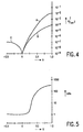
- Fig. 4 plots the current I in amps on the vertical axis as a function of the voltage V applied across a diode.
- Curve A represents the current of a non-programmed diode, with the voltage applied in the forward direction. This state may be regarded as a logic "0".
- a specific value for this current is, for example, 1A/cm 2 .
- the current value may be chosen within certain limits, for example in view of the programming speed. Thus a stronger current may be chosen when the writing speed must be high.
- the difference in the forward current may be a factor 400, which may be used as a logic "1".
- the degradation is probably caused by the generation of defects in the intrinsic Si layer, which defects can be eliminated again through heating. It was found that heating to, for example, 200 °C for 100 minutes causes the diode to exhibit substantially the I-V characteristic A again. This effect can be utilized for erasing the memory.
- Curve C in Fig. 4 shows the I-V characteristic of a diode in the reverse bias state. This characteristic does not change substantially in the case of programming and/or erasing.
- Fig. 5 shows the ratio between the current through the diode in the programmed state and the current in the non-programmed state. As is evident from the drawing, this ratio depends strongly on the voltage and is of the order of 100 for a voltage of 1 V. The ratio is practically equal to 1 in the reverse bias state.
- the memory may be tested after its manufacture in that each ceil is programmed and subsequently the memory is erased in the manner described above. Separate test cells are accordingly not necessary. In addition, it has important advantages for the reliability that the memory cells themselves can be tested.
- the diodes can be monitored during writing, the procedure being stopped when the current through the diode has been sufficiently reduced.
- Fig. 6 is a cross-section of an embodiment of a non-volatile erasable programmable memory according to the invention in which the diodes are formed by p-i-n junctions in ⁇ Si:H. Corresponding components have been given the same reference numerals in Fig. 6 as in Fig. 3c for simplicity's sake.
- the memory matrix is provided on a substrate 3 again and comprises the column lines K 1 , K 2 , K 3 , etc., which extend transversely to the plane of drawing over the substrate. These lines, for example made of Mo again, are covered with strip-shaped lanes of hydrogen-doped ⁇ Si which has been n-type or p-type doped with a suitable impurity.
- the lanes 16 are of the n-type and are doped with As or P atoms in a sufficiently high concentration such that the Mo lines K form conductive junctions with the amorphous Si lanes 16.
- the Mo lanes and the amorphous Si lanes 16 may be patterned in the same manner as the Mo lanes K and the amorphous Si lanes 6 in the preceding embodiment.
- the selection lines R 1 are formed by Mo lanes 10, of which one is shown in the drawing.
- a lane 17 of p-type doped ⁇ Si:H is present below the Mo lane 10, forming an ohmic junction with the Mo of the lane 10.
- the amorphous p-type lane 17 is separated from the amorphous n-type lanes 16 by an interposed strip 8 of amorphous intrinsic (not purposely n-type or p-type doped) Si.
- the layers, 10, 17 and 8 may be formed in the same manner as the layers 10, 9 and 8 in the preceding embodiment.
- a p-i-n diode is formed at each point of intersection between the lines K i and the lines R j (Mo lanes 10).
- amorphous SiGe may be used, i.e. wherein part of the Si atoms are replaced by Ge atoms.
- suitable metals other than Mo may be used for the selection lines.
- a monocrystalline Si substrate may be used as the substrate 3, possibly provided with an integrated circuit comprising, for example, the necessary peripheral electronics for operating the memory.
- memories as described above may be stacked on top of one another in a multilayer structure, planarization layers being provided between the individual layers.
Landscapes
- Semiconductor Memories (AREA)
- Non-Volatile Memory (AREA)
Claims (9)
- Programmierbare, nichtflüchtige Speicheranordnung, PROM, (1), die ein System von programmierbaren, nichtflüchtigen Speicherzellen, M11 - M44, umfasst, die in einer Matrix von Reihen und Spalten angeordnet sind, und mit einem ersten Satz von Selektionsleitungen, K1 - K4, parallel zu den Spalten und einem zweiten Satz von Selektionsleitungen, R1 - R4, parallel zu den Reihen versehen sind, wobei jedem Kreuzungspunkt zwischen den Selektionsleitungen eine Speicherzelle zugeordnet ist, dadurch gekennzeichnet, dass jede Speicherzelle, M11 - M44, ausschließlich durch eine Diode gebildet wird, deren Anode und Kathode leitend mit entsprechenden Selektionsleitungen, K, R, verbunden sind, wobei mindestens eine der Anode und Kathode (8, 9, 16, 17) eine Schicht wasserstoffgesättigtes, Silizium enthaltendes amorphes Halbleitermaterial umfasst.
- Anordnung (1) nach Anspruch 1, dadurch gekennzeichnet, dass die Schicht (8, 9, 16, 17) aus Halbleitermaterial mit den Selektionsleitungen, K, R, am Ort der Kreuzung zwischen den Selektionsleitungen einen Stapel bildet und an der Oberseite mit einer der Selektionsleitungen, R, (10) und an der Unterseite mit der anderen Selektionsleitung, K, welche die erstgenannte Selektionsleitung kreuzt, verbunden ist.
- Anordnung (1) nach Anspruch 1 oder 2, dadurch gekennzeichnet, dass mindestens eine der Selektionsleitungen durch eine Metallbahn gebildet wird und in der die Diode eine Schottky-Diode ist, die zwischen dieser Metallbahn (10) und der Schicht (9) aus Halbleitermaterial angeordnet ist.
- Anordnung (1) nach Anspruch 3, dadurch gekennzeichnet, dass die Metallbahn (10) aus einem Metall der Gruppe: Mo, W, TiW, Cr und Pt hergestellt ist.
- Anordnung (1) nach Anspruch 1 oder 2, dadurch gekennzeichnet, dass die Diode eine pin-Diode ist, die in der Schicht (16, 8, 17) aus Halbleitermaterial gebildet wird.
- Anordnung (1) nach einem der vorhergehenden Ansprüche, dadurch gekennzeichnet, dass die Schicht (8, 9, 16, 17) aus amorphem Halbleitermaterial durch eine Schicht aus wasserstoffgesättigtem amorphem Silizium gebildet wird.
- Verfahren zur Herstellung einer Anordnung (1) nach Anspruch 6, dadurch gekennzeichnet, dass die Schicht (8, 9, 16, 17) aus amorphem Halbleitermaterial mit Hilfe von PECVD bei einer Temperatur von höchstens 400 °C gebildet wird.
- Verfahren nach Anspruch 7, dadurch gekennzeichnet, dass die Depositionstemperatur höchstens ungefähr 250 °C ist.
- Verfahren zum Betreiben einer Anordnung (1) nach einem der Ansprüche 1 bis 6, dadurch gekennzeichnet, dass die Anordnung (1) von einem programmierten Zustand mit Hilfe einer Behandlung bei hoher Temperatur in den Originalzustand gebracht wird.
Priority Applications (1)
| Application Number | Priority Date | Filing Date | Title |
|---|---|---|---|
| EP97918321A EP0842537B1 (de) | 1996-06-05 | 1997-05-22 | Beschreibbares festwertspeicherbauelement und das herstellungsverfahren für solch ein bauelement |
Applications Claiming Priority (4)
| Application Number | Priority Date | Filing Date | Title |
|---|---|---|---|
| EP96201571 | 1996-06-05 | ||
| EP96201571 | 1996-06-05 | ||
| EP97918321A EP0842537B1 (de) | 1996-06-05 | 1997-05-22 | Beschreibbares festwertspeicherbauelement und das herstellungsverfahren für solch ein bauelement |
| PCT/IB1997/000582 WO1997047041A2 (en) | 1996-06-05 | 1997-05-22 | Programmable, non-volatile memory device, and method of manufacturing such a device |
Publications (2)
| Publication Number | Publication Date |
|---|---|
| EP0842537A2 EP0842537A2 (de) | 1998-05-20 |
| EP0842537B1 true EP0842537B1 (de) | 2005-08-24 |
Family
ID=8224055
Family Applications (1)
| Application Number | Title | Priority Date | Filing Date |
|---|---|---|---|
| EP97918321A Expired - Lifetime EP0842537B1 (de) | 1996-06-05 | 1997-05-22 | Beschreibbares festwertspeicherbauelement und das herstellungsverfahren für solch ein bauelement |
Country Status (5)
| Country | Link |
|---|---|
| US (1) | US6291836B1 (de) |
| EP (1) | EP0842537B1 (de) |
| JP (1) | JP4148995B2 (de) |
| DE (1) | DE69734050T2 (de) |
| WO (1) | WO1997047041A2 (de) |
Families Citing this family (81)
| Publication number | Priority date | Publication date | Assignee | Title |
|---|---|---|---|---|
| US7157314B2 (en) | 1998-11-16 | 2007-01-02 | Sandisk Corporation | Vertically stacked field programmable nonvolatile memory and method of fabrication |
| US6631085B2 (en) * | 2000-04-28 | 2003-10-07 | Matrix Semiconductor, Inc. | Three-dimensional memory array incorporating serial chain diode stack |
| WO2001084553A2 (en) * | 2000-04-28 | 2001-11-08 | Matrix Semiconductor, Inc. | Three-dimensional memory array and method of fabrication |
| US8575719B2 (en) * | 2000-04-28 | 2013-11-05 | Sandisk 3D Llc | Silicon nitride antifuse for use in diode-antifuse memory arrays |
| US6618295B2 (en) * | 2001-03-21 | 2003-09-09 | Matrix Semiconductor, Inc. | Method and apparatus for biasing selected and unselected array lines when writing a memory array |
| US6504746B2 (en) * | 2001-05-31 | 2003-01-07 | Hewlett-Packard Company | High-density low-cost read-only memory circuit |
| US6646912B2 (en) * | 2001-06-05 | 2003-11-11 | Hewlett-Packard Development Company, Lp. | Non-volatile memory |
| US6599796B2 (en) * | 2001-06-29 | 2003-07-29 | Hewlett-Packard Development Company, L.P. | Apparatus and fabrication process to reduce crosstalk in pirm memory array |
| US6535418B2 (en) * | 2001-07-24 | 2003-03-18 | Hewlett-Packard Development Company, Llp | Optically programmable address logic for solid state diode-based memory |
| US20070164388A1 (en) * | 2002-12-19 | 2007-07-19 | Sandisk 3D Llc | Memory cell comprising a diode fabricated in a low resistivity, programmed state |
| US7005350B2 (en) * | 2002-12-31 | 2006-02-28 | Matrix Semiconductor, Inc. | Method for fabricating programmable memory array structures incorporating series-connected transistor strings |
| US7505321B2 (en) * | 2002-12-31 | 2009-03-17 | Sandisk 3D Llc | Programmable memory array structure incorporating series-connected transistor strings and methods for fabrication and operation of same |
| US7233522B2 (en) * | 2002-12-31 | 2007-06-19 | Sandisk 3D Llc | NAND memory array incorporating capacitance boosting of channel regions in unselected memory cells and method for operation of same |
| JP2004319587A (ja) * | 2003-04-11 | 2004-11-11 | Sharp Corp | メモリセル、メモリ装置及びメモリセル製造方法 |
| US7177183B2 (en) | 2003-09-30 | 2007-02-13 | Sandisk 3D Llc | Multiple twin cell non-volatile memory array and logic block structure and method therefor |
| US20050128807A1 (en) * | 2003-12-05 | 2005-06-16 | En-Hsing Chen | Nand memory array incorporating multiple series selection devices and method for operation of same |
| US7023739B2 (en) * | 2003-12-05 | 2006-04-04 | Matrix Semiconductor, Inc. | NAND memory array incorporating multiple write pulse programming of individual memory cells and method for operation of same |
| US7221588B2 (en) * | 2003-12-05 | 2007-05-22 | Sandisk 3D Llc | Memory array incorporating memory cells arranged in NAND strings |
| US20060067117A1 (en) * | 2004-09-29 | 2006-03-30 | Matrix Semiconductor, Inc. | Fuse memory cell comprising a diode, the diode serving as the fuse element |
| US10134985B2 (en) * | 2006-10-20 | 2018-11-20 | The Regents Of The University Of Michigan | Non-volatile solid state resistive switching devices |
| WO2010048127A2 (en) | 2008-10-20 | 2010-04-29 | The Regents Of The University Of Michigan | A silicon based nanoscale crossbar memory |
| US9608119B2 (en) * | 2010-03-02 | 2017-03-28 | Micron Technology, Inc. | Semiconductor-metal-on-insulator structures, methods of forming such structures, and semiconductor devices including such structures |
| US9012307B2 (en) | 2010-07-13 | 2015-04-21 | Crossbar, Inc. | Two terminal resistive switching device structure and method of fabricating |
| US9570678B1 (en) | 2010-06-08 | 2017-02-14 | Crossbar, Inc. | Resistive RAM with preferental filament formation region and methods |
| US8946046B1 (en) | 2012-05-02 | 2015-02-03 | Crossbar, Inc. | Guided path for forming a conductive filament in RRAM |
| US9601692B1 (en) | 2010-07-13 | 2017-03-21 | Crossbar, Inc. | Hetero-switching layer in a RRAM device and method |
| US8441835B2 (en) | 2010-06-11 | 2013-05-14 | Crossbar, Inc. | Interface control for improved switching in RRAM |
| JP5981424B2 (ja) | 2010-06-11 | 2016-08-31 | クロスバー, インコーポレイテッドCrossbar, Inc. | メモリー素子に関する柱状構造及び方法 |
| US8374018B2 (en) | 2010-07-09 | 2013-02-12 | Crossbar, Inc. | Resistive memory using SiGe material |
| US8884261B2 (en) | 2010-08-23 | 2014-11-11 | Crossbar, Inc. | Device switching using layered device structure |
| US8569172B1 (en) | 2012-08-14 | 2013-10-29 | Crossbar, Inc. | Noble metal/non-noble metal electrode for RRAM applications |
| US8947908B2 (en) | 2010-11-04 | 2015-02-03 | Crossbar, Inc. | Hetero-switching layer in a RRAM device and method |
| US8467227B1 (en) | 2010-11-04 | 2013-06-18 | Crossbar, Inc. | Hetero resistive switching material layer in RRAM device and method |
| US8168506B2 (en) | 2010-07-13 | 2012-05-01 | Crossbar, Inc. | On/off ratio for non-volatile memory device and method |
| US8569734B2 (en) * | 2010-08-04 | 2013-10-29 | Micron Technology, Inc. | Forming resistive random access memories together with fuse arrays |
| US9401475B1 (en) | 2010-08-23 | 2016-07-26 | Crossbar, Inc. | Method for silver deposition for a non-volatile memory device |
| US8889521B1 (en) | 2012-09-14 | 2014-11-18 | Crossbar, Inc. | Method for silver deposition for a non-volatile memory device |
| US8492195B2 (en) | 2010-08-23 | 2013-07-23 | Crossbar, Inc. | Method for forming stackable non-volatile resistive switching memory devices |
| US8404553B2 (en) | 2010-08-23 | 2013-03-26 | Crossbar, Inc. | Disturb-resistant non-volatile memory device and method |
| US8391049B2 (en) | 2010-09-29 | 2013-03-05 | Crossbar, Inc. | Resistor structure for a non-volatile memory device and method |
| US8558212B2 (en) | 2010-09-29 | 2013-10-15 | Crossbar, Inc. | Conductive path in switching material in a resistive random access memory device and control |
| US8502185B2 (en) | 2011-05-31 | 2013-08-06 | Crossbar, Inc. | Switching device having a non-linear element |
| USRE46335E1 (en) | 2010-11-04 | 2017-03-07 | Crossbar, Inc. | Switching device having a non-linear element |
| US8088688B1 (en) | 2010-11-05 | 2012-01-03 | Crossbar, Inc. | p+ polysilicon material on aluminum for non-volatile memory device and method |
| US8930174B2 (en) | 2010-12-28 | 2015-01-06 | Crossbar, Inc. | Modeling technique for resistive random access memory (RRAM) cells |
| US8791010B1 (en) | 2010-12-31 | 2014-07-29 | Crossbar, Inc. | Silver interconnects for stacked non-volatile memory device and method |
| US8815696B1 (en) | 2010-12-31 | 2014-08-26 | Crossbar, Inc. | Disturb-resistant non-volatile memory device using via-fill and etchback technique |
| US9153623B1 (en) | 2010-12-31 | 2015-10-06 | Crossbar, Inc. | Thin film transistor steering element for a non-volatile memory device |
| US8952418B2 (en) | 2011-03-01 | 2015-02-10 | Micron Technology, Inc. | Gated bipolar junction transistors |
| US8450710B2 (en) | 2011-05-27 | 2013-05-28 | Crossbar, Inc. | Low temperature p+ silicon junction material for a non-volatile memory device |
| US9620206B2 (en) | 2011-05-31 | 2017-04-11 | Crossbar, Inc. | Memory array architecture with two-terminal memory cells |
| US8394670B2 (en) | 2011-05-31 | 2013-03-12 | Crossbar, Inc. | Vertical diodes for non-volatile memory device |
| US8619459B1 (en) | 2011-06-23 | 2013-12-31 | Crossbar, Inc. | High operating speed resistive random access memory |
| US8946669B1 (en) | 2012-04-05 | 2015-02-03 | Crossbar, Inc. | Resistive memory device and fabrication methods |
| US9627443B2 (en) | 2011-06-30 | 2017-04-18 | Crossbar, Inc. | Three-dimensional oblique two-terminal memory with enhanced electric field |
| US8659929B2 (en) | 2011-06-30 | 2014-02-25 | Crossbar, Inc. | Amorphous silicon RRAM with non-linear device and operation |
| US9166163B2 (en) | 2011-06-30 | 2015-10-20 | Crossbar, Inc. | Sub-oxide interface layer for two-terminal memory |
| US9564587B1 (en) | 2011-06-30 | 2017-02-07 | Crossbar, Inc. | Three-dimensional two-terminal memory with enhanced electric field and segmented interconnects |
| WO2013015776A1 (en) | 2011-07-22 | 2013-01-31 | Crossbar, Inc. | Seed layer for a p + silicon germanium material for a non-volatile memory device and method |
| US8674724B2 (en) | 2011-07-29 | 2014-03-18 | Crossbar, Inc. | Field programmable gate array utilizing two-terminal non-volatile memory |
| US10056907B1 (en) | 2011-07-29 | 2018-08-21 | Crossbar, Inc. | Field programmable gate array utilizing two-terminal non-volatile memory |
| US9729155B2 (en) | 2011-07-29 | 2017-08-08 | Crossbar, Inc. | Field programmable gate array utilizing two-terminal non-volatile memory |
| US8716098B1 (en) | 2012-03-09 | 2014-05-06 | Crossbar, Inc. | Selective removal method and structure of silver in resistive switching device for a non-volatile memory device |
| US9087576B1 (en) | 2012-03-29 | 2015-07-21 | Crossbar, Inc. | Low temperature fabrication method for a three-dimensional memory device and structure |
| US9685608B2 (en) | 2012-04-13 | 2017-06-20 | Crossbar, Inc. | Reduced diffusion in metal electrode for two-terminal memory |
| US8658476B1 (en) | 2012-04-20 | 2014-02-25 | Crossbar, Inc. | Low temperature P+ polycrystalline silicon material for non-volatile memory device |
| US8796658B1 (en) | 2012-05-07 | 2014-08-05 | Crossbar, Inc. | Filamentary based non-volatile resistive memory device and method |
| US8765566B2 (en) | 2012-05-10 | 2014-07-01 | Crossbar, Inc. | Line and space architecture for a non-volatile memory device |
| US9583701B1 (en) | 2012-08-14 | 2017-02-28 | Crossbar, Inc. | Methods for fabricating resistive memory device switching material using ion implantation |
| US9741765B1 (en) | 2012-08-14 | 2017-08-22 | Crossbar, Inc. | Monolithically integrated resistive memory using integrated-circuit foundry compatible processes |
| US8946673B1 (en) | 2012-08-24 | 2015-02-03 | Crossbar, Inc. | Resistive switching device structure with improved data retention for non-volatile memory device and method |
| US9312483B2 (en) | 2012-09-24 | 2016-04-12 | Crossbar, Inc. | Electrode structure for a non-volatile memory device and method |
| US9576616B2 (en) | 2012-10-10 | 2017-02-21 | Crossbar, Inc. | Non-volatile memory with overwrite capability and low write amplification |
| US11068620B2 (en) | 2012-11-09 | 2021-07-20 | Crossbar, Inc. | Secure circuit integrated with memory layer |
| US8982647B2 (en) | 2012-11-14 | 2015-03-17 | Crossbar, Inc. | Resistive random access memory equalization and sensing |
| US9412790B1 (en) | 2012-12-04 | 2016-08-09 | Crossbar, Inc. | Scalable RRAM device architecture for a non-volatile memory device and method |
| US9406379B2 (en) | 2013-01-03 | 2016-08-02 | Crossbar, Inc. | Resistive random access memory with non-linear current-voltage relationship |
| US9324942B1 (en) | 2013-01-31 | 2016-04-26 | Crossbar, Inc. | Resistive memory cell with solid state diode |
| US9112145B1 (en) | 2013-01-31 | 2015-08-18 | Crossbar, Inc. | Rectified switching of two-terminal memory via real time filament formation |
| US8934280B1 (en) | 2013-02-06 | 2015-01-13 | Crossbar, Inc. | Capacitive discharge programming for two-terminal memory cells |
| US10290801B2 (en) | 2014-02-07 | 2019-05-14 | Crossbar, Inc. | Scalable silicon based resistive memory device |
Family Cites Families (11)
| Publication number | Priority date | Publication date | Assignee | Title |
|---|---|---|---|---|
| US3530441A (en) * | 1969-01-15 | 1970-09-22 | Energy Conversion Devices Inc | Method and apparatus for storing and retrieving information |
| IL61678A (en) * | 1979-12-13 | 1984-04-30 | Energy Conversion Devices Inc | Programmable cell and programmable electronic arrays comprising such cells |
| US4396998A (en) * | 1980-08-27 | 1983-08-02 | Mobay Chemical Corporation | Thermally reprogrammable memory array and a thermally reprogrammable memory cell therefor |
| US4442507A (en) * | 1981-02-23 | 1984-04-10 | Burroughs Corporation | Electrically programmable read-only memory stacked above a semiconductor substrate |
| US4545111A (en) * | 1983-01-18 | 1985-10-08 | Energy Conversion Devices, Inc. | Method for making, parallel preprogramming or field programming of electronic matrix arrays |
| US4868616A (en) * | 1986-12-11 | 1989-09-19 | Energy Conversion Devices, Inc. | Amorphous electronic matrix array for liquid crystal display |
| GB8910854D0 (en) * | 1989-05-11 | 1989-06-28 | British Petroleum Co Plc | Semiconductor device |
| US5502315A (en) * | 1989-09-07 | 1996-03-26 | Quicklogic Corporation | Electrically programmable interconnect structure having a PECVD amorphous silicon element |
| US5404007A (en) * | 1992-05-29 | 1995-04-04 | The United States Of America As Represented By The Secretary Of The Air Force | Radiation resistant RLG detector systems |
| EP0749638B1 (de) * | 1994-12-22 | 1999-06-16 | Koninklijke Philips Electronics N.V. | Halbleiterspeicheranordnungen und herstellungsverfahren |
| US5835396A (en) * | 1996-10-17 | 1998-11-10 | Zhang; Guobiao | Three-dimensional read-only memory |
-
1997
- 1997-05-22 WO PCT/IB1997/000582 patent/WO1997047041A2/en not_active Ceased
- 1997-05-22 DE DE69734050T patent/DE69734050T2/de not_active Expired - Fee Related
- 1997-05-22 JP JP50035998A patent/JP4148995B2/ja not_active Expired - Fee Related
- 1997-05-22 EP EP97918321A patent/EP0842537B1/de not_active Expired - Lifetime
- 1997-05-30 US US08/866,649 patent/US6291836B1/en not_active Expired - Lifetime
Also Published As
| Publication number | Publication date |
|---|---|
| JP4148995B2 (ja) | 2008-09-10 |
| EP0842537A2 (de) | 1998-05-20 |
| US6291836B1 (en) | 2001-09-18 |
| JPH11510966A (ja) | 1999-09-21 |
| DE69734050T2 (de) | 2006-06-08 |
| WO1997047041A2 (en) | 1997-12-11 |
| DE69734050D1 (de) | 2005-09-29 |
| WO1997047041A3 (en) | 1998-01-22 |
Similar Documents
| Publication | Publication Date | Title |
|---|---|---|
| EP0842537B1 (de) | Beschreibbares festwertspeicherbauelement und das herstellungsverfahren für solch ein bauelement | |
| US4499557A (en) | Programmable cell for use in programmable electronic arrays | |
| US7764534B2 (en) | Two terminal nonvolatile memory using gate controlled diode elements | |
| US4569121A (en) | Method of fabricating a programmable read-only memory cell incorporating an antifuse utilizing deposition of amorphous semiconductor layer | |
| US7682920B2 (en) | Method for making a p-i-n diode crystallized adjacent to a silicide in series with a dielectric antifuse | |
| EP0680087B1 (de) | Halbleiterbauelement und Methode, welche eine Silizidreaktion ausnutzen, um anpassbare Verbindungen herzustellen | |
| US4599705A (en) | Programmable cell for use in programmable electronic arrays | |
| US5311039A (en) | PROM and ROM memory cells | |
| US8330250B2 (en) | P-I-N diode crystallized adjacent to a silicide in series with a dielectric material | |
| US7706177B2 (en) | Method of programming cross-point diode memory array | |
| US4922319A (en) | Semiconductor programmable memory device | |
| US7855119B2 (en) | Method for forming polycrystalline thin film bipolar transistors | |
| KR900002912B1 (ko) | 전자 매트릭스 어레이(eletronic matrix array) 및 그 제조방법 | |
| US4455495A (en) | Programmable semiconductor integrated circuitry including a programming semiconductor element | |
| US20060067117A1 (en) | Fuse memory cell comprising a diode, the diode serving as the fuse element | |
| US20060249753A1 (en) | High-density nonvolatile memory array fabricated at low temperature comprising semiconductor diodes | |
| US20070090425A1 (en) | Memory cell comprising switchable semiconductor memory element with trimmable resistance | |
| JPS59168665A (ja) | 半導体メモリ装置およびその製造方法 | |
| US20090085154A1 (en) | Vertical diode based memory cells having a lowered programming voltage and methods of forming the same | |
| US7800939B2 (en) | Method of making 3D R/W cell with reduced reverse leakage | |
| KR20090089320A (ko) | 유전체 안티휴즈와 직렬로 실리사이드에 인접하여 결정화된 p-i-n 다이오드와 이를 형성하는 방법 | |
| US7759666B2 (en) | 3D R/W cell with reduced reverse leakage | |
| US5272671A (en) | Semiconductor memory device with redundancy structure and process of repairing same | |
| US20080308903A1 (en) | Polycrystalline thin film bipolar transistors | |
| CN119156004A (zh) | 存储器器件及其制造方法 |
Legal Events
| Date | Code | Title | Description |
|---|---|---|---|
| PUAI | Public reference made under article 153(3) epc to a published international application that has entered the european phase |
Free format text: ORIGINAL CODE: 0009012 |
|
| AK | Designated contracting states |
Kind code of ref document: A2 Designated state(s): DE FR GB IT NL |
|
| RAP3 | Party data changed (applicant data changed or rights of an application transferred) |
Owner name: KONINKLIJKE PHILIPS ELECTRONICS N.V. |
|
| 17P | Request for examination filed |
Effective date: 19980722 |
|
| 17Q | First examination report despatched |
Effective date: 20031125 |
|
| GRAP | Despatch of communication of intention to grant a patent |
Free format text: ORIGINAL CODE: EPIDOSNIGR1 |
|
| GRAS | Grant fee paid |
Free format text: ORIGINAL CODE: EPIDOSNIGR3 |
|
| GRAA | (expected) grant |
Free format text: ORIGINAL CODE: 0009210 |
|
| AK | Designated contracting states |
Kind code of ref document: B1 Designated state(s): DE FR GB IT NL |
|
| PG25 | Lapsed in a contracting state [announced via postgrant information from national office to epo] |
Ref country code: NL Free format text: LAPSE BECAUSE OF FAILURE TO SUBMIT A TRANSLATION OF THE DESCRIPTION OR TO PAY THE FEE WITHIN THE PRESCRIBED TIME-LIMIT Effective date: 20050824 |
|
| REG | Reference to a national code |
Ref country code: GB Ref legal event code: FG4D |
|
| REG | Reference to a national code |
Ref country code: GB Ref legal event code: 746 Effective date: 20050905 |
|
| REF | Corresponds to: |
Ref document number: 69734050 Country of ref document: DE Date of ref document: 20050929 Kind code of ref document: P |
|
| NLV1 | Nl: lapsed or annulled due to failure to fulfill the requirements of art. 29p and 29m of the patents act | ||
| ET | Fr: translation filed | ||
| PLBE | No opposition filed within time limit |
Free format text: ORIGINAL CODE: 0009261 |
|
| STAA | Information on the status of an ep patent application or granted ep patent |
Free format text: STATUS: NO OPPOSITION FILED WITHIN TIME LIMIT |
|
| 26N | No opposition filed |
Effective date: 20060526 |
|
| REG | Reference to a national code |
Ref country code: GB Ref legal event code: 732E |
|
| REG | Reference to a national code |
Ref country code: FR Ref legal event code: TP |
|
| PGFP | Annual fee paid to national office [announced via postgrant information from national office to epo] |
Ref country code: IT Payment date: 20080530 Year of fee payment: 11 |
|
| PG25 | Lapsed in a contracting state [announced via postgrant information from national office to epo] |
Ref country code: IT Free format text: LAPSE BECAUSE OF NON-PAYMENT OF DUE FEES Effective date: 20080522 |
|
| PGFP | Annual fee paid to national office [announced via postgrant information from national office to epo] |
Ref country code: FR Payment date: 20090515 Year of fee payment: 13 Ref country code: DE Payment date: 20090514 Year of fee payment: 13 |
|
| PGFP | Annual fee paid to national office [announced via postgrant information from national office to epo] |
Ref country code: GB Payment date: 20100329 Year of fee payment: 14 |
|
| REG | Reference to a national code |
Ref country code: FR Ref legal event code: ST Effective date: 20110131 |
|
| PG25 | Lapsed in a contracting state [announced via postgrant information from national office to epo] |
Ref country code: DE Free format text: LAPSE BECAUSE OF NON-PAYMENT OF DUE FEES Effective date: 20101201 |
|
| PG25 | Lapsed in a contracting state [announced via postgrant information from national office to epo] |
Ref country code: FR Free format text: LAPSE BECAUSE OF NON-PAYMENT OF DUE FEES Effective date: 20100531 |
|
| GBPC | Gb: european patent ceased through non-payment of renewal fee |
Effective date: 20120522 |
|
| PG25 | Lapsed in a contracting state [announced via postgrant information from national office to epo] |
Ref country code: GB Free format text: LAPSE BECAUSE OF NON-PAYMENT OF DUE FEES Effective date: 20120522 |