EP0843343A2 - Verarbeitungssystem - Google Patents
Verarbeitungssystem Download PDFInfo
- Publication number
- EP0843343A2 EP0843343A2 EP97120153A EP97120153A EP0843343A2 EP 0843343 A2 EP0843343 A2 EP 0843343A2 EP 97120153 A EP97120153 A EP 97120153A EP 97120153 A EP97120153 A EP 97120153A EP 0843343 A2 EP0843343 A2 EP 0843343A2
- Authority
- EP
- European Patent Office
- Prior art keywords
- substrate
- machine
- wafer
- processing
- processing system
- Prior art date
- Legal status (The legal status is an assumption and is not a legal conclusion. Google has not performed a legal analysis and makes no representation as to the accuracy of the status listed.)
- Granted
Links
Images


Classifications
-
- H—ELECTRICITY
- H10—SEMICONDUCTOR DEVICES; ELECTRIC SOLID-STATE DEVICES NOT OTHERWISE PROVIDED FOR
- H10P—GENERIC PROCESSES OR APPARATUS FOR THE MANUFACTURE OR TREATMENT OF DEVICES COVERED BY CLASS H10
- H10P72/00—Handling or holding of wafers, substrates or devices during manufacture or treatment thereof
- H10P72/30—Handling or holding of wafers, substrates or devices during manufacture or treatment thereof for conveying, e.g. between different workstations
- H10P72/34—Handling or holding of wafers, substrates or devices during manufacture or treatment thereof for conveying, e.g. between different workstations the wafers being stored in a carrier, involving loading and unloading
- H10P72/3411—Handling or holding of wafers, substrates or devices during manufacture or treatment thereof for conveying, e.g. between different workstations the wafers being stored in a carrier, involving loading and unloading involving loading and unloading of wafers
-
- Y—GENERAL TAGGING OF NEW TECHNOLOGICAL DEVELOPMENTS; GENERAL TAGGING OF CROSS-SECTIONAL TECHNOLOGIES SPANNING OVER SEVERAL SECTIONS OF THE IPC; TECHNICAL SUBJECTS COVERED BY FORMER USPC CROSS-REFERENCE ART COLLECTIONS [XRACs] AND DIGESTS
- Y10—TECHNICAL SUBJECTS COVERED BY FORMER USPC
- Y10S—TECHNICAL SUBJECTS COVERED BY FORMER USPC CROSS-REFERENCE ART COLLECTIONS [XRACs] AND DIGESTS
- Y10S414/00—Material or article handling
- Y10S414/135—Associated with semiconductor wafer handling
- Y10S414/136—Associated with semiconductor wafer handling including wafer orienting means
Definitions
- a substrate such as a semiconductor wafer (hereinafter, refereed to as a wafer)
- a photoresist solution to form a photoresist film.
- the exposed film is developed with a developing solution.
- a photoresist coating and developing system has been used.
- a brushing machine for brushing a wafer while turning it, a washing machine for washing a wafer W with a high-pressure jet of water, an adhesion processing machine for improving the fixation of resist by subjecting the surface of the wafer to an adhesion process, a cooling machine for cooling the wafer to a specific temperature, a photoresist coating machine for coating the surface of the rotating wafer with a resist solution, a heater for heating the photoresist-coated wafer or the pattern-exposed wafer, and a developing machine for developing the exposed wafer by supplying a developing solution to the wafer's surface, while rotating the wafer.
- the loading/unloading arm in the exposure machine is designed to advance to and retreat from the interface section and thereby load the wafer in the interface section into the exposure machine and returns the exposed wafer in the machine to the interface section.
- the object of the present invention is to provide a processing system capable of not only dealing with transfer means, such as various types of transfer arms in an external machine but also realizing smooth transfer and saving the installation space.
- the substrate table unit has first and second tables that are laid one on top of the other and can move up and down and stop at a specific height, the first table allowing the substrate to be temporarily placed on it in transferring the substrate to the external processing machine, the second table allowing the substrate to be temporarily placed on it in receiving the substrate from the external processing machine.
- the transfer unit transfers the substrate between the first and second tables and at least one of the internal processing machines.
- the first table used in transferring the processed substrate to the external processing machine and the second table used in receiving the substrate from the external processing machine are provided independently in the substrate table unit, which enables the transfer unit in the external processing machine to transfer the substrate smoothly. Furthermore, because the first table and second table are laid one on top of the other and the substrate table unit on which those wafer tables are installed can move up and down freely, the substrate can be loaded onto and unloaded from the first wafer table and second wafer table in the same delivery position. The arrangement of the first and second tables helps minimize the space necessary for the installation of the system.
- a processing system comprising a plurality of types of internal processing machines that perform various processes on a substrate, and an interface section that delivers and receives the substrate to and from an external processing machine for performing a specific process on the substrate, wherein the interface section includes a transfer unit for taking in the substrate from at least one of the internal processing machines and transferring the substrate to the external processing machine and a substrate table unit for temporarily holding the substrate in transferring the substrate between the internal processing machine and the external processing machine via the transfer unit.
- the substrate table unit has first and second tables that are laid one on top of the other and can move up and down and stop at a specific height.
- Each of the first and second tables has two placement tables side by side that allow two substrates to be temporarily placed on them in transferring a substrate between the external processing machine and the internal processing machine.
- the transfer unit transfers the substrate between the first and second tables and at least one of the internal processing machines.
- each of the upper stage and lower stage of the substrate table unit has the first and second tables side by side. This enables the transfer unit in the external processing machine to deliver the unprocessed substrate to the external processing machine and receives the processed from the external processing machine by means of the same substrate table unit at the same height.
- the substrate table unit can be moved up and down suitably to place the substrate on any empty table, thereby allowing the substrate to wait for processing.
- an empty table can be used as a standby area in the processing system of the first aspect, and the number of standby areas is increased in the processing system of the second aspect.
- the first wafer table or second wafer table is designed to further perform an exposure process on the substrate, for example, a peripheral exposure process on a substrate, such as a semiconductor wafer
- a peripheral exposure process on a substrate such as a semiconductor wafer
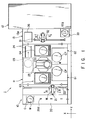
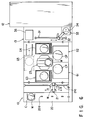
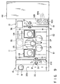
- five processing machine groups G1, G2, G3, G4, and G5 can be arranged.
- a first and second processing machine groups G1 and G2 are arranged in the front of the system (i.e., in the lower part of FIG. 1).
- a third processing machine group G3 is arranged adjacent to the cassette station 10.
- a fourth processing machine group G4 is put adjacent to the interface section 13.
- a fifth processing group G5 is arranged at the back of the system.
- the third processing machine group G3 open-type processing machines are laid one on top of another in eight stages as shown in FIG. 3. These machines perform specific processes on the wafer W on a table (not shown).
- a cooling machine (COL) for cooling the wafer
- an adhesion processing machine (AD) for improving the fixation of resist by dehydrating the surface of the wafer
- an alignment machine (ALIM) for aligning the wafer
- EXT extension machine
- PREBAKE pre-baking machines
- POBAKE post-baking machines
- the fifth processing machine group G5 represented by a broken line can be arranged at the back of the main transfer machine 23 as described above.
- the multistage processing machine in the fifth processing machine group G5 can move sideward along a guide rail 24 when viewed from the main wafer transfer machine 23. Therefore, even when the multistage processing machine in the fifth processing machine group G5 is provided at the back of the main wafer transfer machine 23 as shown in the figure, sliding the fifth processing machine group G5 along the guide rail 24 secures a space at the back of the main wafer transfer machine 23, which facilitates the maintenance of the main wafer transfer machine 23 from behind the system.
- the multistage processing machine in the fifth processing machine group G5 may turn outward from the system as shown by dot-dash lines in FIG. 1.
- the pivotal movement also makes it easy to secure a space for the maintenance of the main wafer transfer machine 23.
- the main wafer transfer machine 23 can not only move vertically but also rotate in the direction of ⁇ , it can access each unit in the first to fifth processing machine groups G1, G2, G3, G4, and G5.
- the main wafer transfer machine 23 has three pairs of tweezers 23a that hold a wafer directly. The three pairs of tweezers are laid one on top of another. Using any pair of tweezers 23a, the main wafer transfer machine can load and unload a wafer into or from each machine in the first to fifth processing machine groups G1, G2, G3, G4, and G5.
- a filter unit 25 composed of a high-performance filter, such as a ULPA filter (Ultra Low Penetrate Air filter), or a chemical filter is provided in each of the cassette station 10, processing station 11, and interface section 13 in the upper part of the system as shown in FIG. 2.
- a filter unit 25 composed of a high-performance filter, such as a ULPA filter (Ultra Low Penetrate Air filter), or a chemical filter is provided in each of the cassette station 10, processing station 11, and interface section 13 in the upper part of the system as shown in FIG. 2.
- ULPA filter Ultra Low Penetrate Air filter
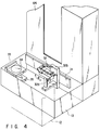
- a substrate table unit 33 is provided in the front of the base 13a and at its one end close to the exposure device 12. As shown in FIGS. 4, 5A and 5B, the substrate table unit 33 has a first wafer table 34 at the upper stage and a second wafer table 35 at the lower stage. It can make an up-and-down movement by means of a suitable driving mechanism (not shown) and stop at any height.
- the substrate table unit 33 is located in a position where the transfer arm 12a, serving as the transfer means of the exposure machine 12, can access the table unit. Specifically, the substrate table unit is located in such a position as enables the transfer arm 12a to receive the wafer placed in the specific place of the substrate table unit 33 or place the transferred wafer W in a specific place of the substrate table unit 33.
- the first wafer table 34 has basically the same structure as that of the second wafer table 35. A detailed explanation of the first wafer table 34 will be given.
- the first wafer table 34 includes a support base 34a part of which is stuck to an up-and-down support means (i.e., an elevator post) 33a that moves up and down by means of the driving mechanism, a plurality of periphery support members 34b that are provided on the support base 34a and support the periphery of the wafer W, and a suitable number of support pins 34c provided in the vicinity of the center of the support base 34a. As shown in FIG.
- the support pins 34c support the wafer W in the vicinity of the wafer's center and the periphery support members 34b support the wafer's periphery. Being supported this way, the wafer is placed on the first wafer table 34.
- the second wafer table 35 includes a support table 35a, periphery support members 35b, and support pins 35c.
- a peripheral exposure machine 36 that performs a peripheral exposure process on the wafer W is provided at the end of the base 13a of the interface section 13 opposite to the substrate table unit 33, specifically at the back of the system.
- the wafer carriage 32 can also access the peripheral exposure machine 36.
- the wafer carriage 21 accesses a cassette C that houses unprocessed wafers on the cassette table 20 and takes out a wafer W from the cassette C. Then, the wafer carriage 21 moves to the alignment machine (ALIM) located in the multistage machine in the third processing machine group G3 of the processing station 11 and delivers the wafer W to the alignment machine (ALIM).
- ALIM alignment machine
- the aligned wafer W is received by the main wafer transfer machine 23.
- the main wafer transfer machine 23 move to the front of the adhesion processing machine (AD) located at the lower stage of the alignment machine (ALIM) in the third processing machine group G3 and loads the wafer W into the adhesion processing machine. Then, the main wafer transfer machine 23 loads the wafer into the cooling machine (COL) belonging to the multistage machine in the third processing machine group G3 or the fourth processing machine group G4.
- the wafer W is heated to the setting temperature before the photoresist coating process, for example, 23°C in the cooling machine (COL).
- the main wafer transfer machine 23 unloads the wafer W from the cooling machine (COL), replaces it with another wafer W held therein, and loads the cooled wafer W into the photoresist coating machine (COT) belonging to the multistage machine in the first processing machine group G1 or the second processing machine group G2.
- the photoresist coating machine (COT) the wafer W is coated with a photoresist solution by a spin coating method to form a thick film on the wafer's surface.
- the wafer main transfer machine 23 unloads the wafer W from the photoresist coating machine (COT) and loads it into the pre-baking machine (PREBAKE).
- the wafer W is heated at a specific temperature, for example, 100°C for a specific time to evaporate the remaining solvent from the coated film on the wafer W.
- the main wafer transfer machine 23 unloads the wafer W from the pre-baking machine (PREBAKE) and loads it into the extension/cooling machine (EXTTCOL) belonging to the multistage machine in the fourth processing machine group G4.
- the wafer W is cooled to a temperature suitable for the next step, that is, the peripheral exposure process at the peripheral exposure machine 36, for example, to 24°C.
- the main wafer transfer machine 23 transfers the wafer to the extension machine (EXT) just above and places the wafer W on a specific table (not shown) in the extension machine (EXT).
- the wafer carriage 32 of the interface section 13 accesses the table from the opposite side and receives the wafer W.
- the wafer carriage 32 loads the wafer W into the peripheral exposure machine 36 of the interface section 12.
- the peripheral exposure machine 36 performs an exposure process on the periphery of the wafer W.
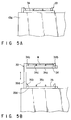
- the wafer carriage 32 unloads the wafer W from the peripheral exposure machine 36 and places the wafer W on the first wafer table 34 at the upper stage of the substrate table unit 33.
- the wafer carriage 32 moves over the transfer path 31 along the substrate table unit and places the wafer on the first wafer table 34 in a specific position on the transfer path.
- the wafer carriage 32 accesses the first wafer table 34 obliquely, not face-to-face, and places the wafer W on the first wafer table 34 as shown in FIG. 6.
- the step motor provided on the drive mechanism 32b shown in FIG.
- the control signal from a controller (not shown) so that the arm 21 of the wafer carriage 32 can access the first wafer table 34 obliquely.
- the wafer W is placed on the first wafer table 34 faster than when the wafer carriage 32 is moved to the face-to-face position with the first wafer table 34.
- the substrate table unit 33 rises as shown in FIG. 5B and waits for the transfer arm 12a of the exposure machine 12 to access the unit. Specifically, the substrate table unit waits for the transfer arm 12a of the exposure machine 12 to transfer the wafer W subjected to the specific pattern exposure process at the exposure machine 12. After the transfer arm 12a of the exposure machine 12 has placed the exposed wafer W on the second wafer table 35 and temporarily retreated, the substrate table unit 33 goes down to the position shown in FIG. 4.
- the transfer arm 12a of the exposure machine 12 receives the wafer W that is placed on the first wafer table 34 and waits for pattern exposure. The transfer arm then retreats into the exposure machine 12, which performs a specific pattern exposure process on the wafer W.
- the substrate table unit 33 rises again to the position shown in FIG. 5.
- the wafer carriage 32 receives the exposed wafer W on the second table 35 and transfers it to the extension machine (EXT).
- EXT extension machine
- POBAKE post-baking machine
- the substrate table unit 33 that relays the transfer has the first wafer table 34 on which the wafer W transferred from the system is placed, or the OUT-side wafer table, at the upper stage, and the second wafer table 35 on which the wafer to be transferred to the system is placed, or the IN-side wafer table, at the lower stage.
- the substrate table unit is designed to move vertically.
- the OUT-side wafer table and the IN-side wafer table are laid one on top of the other. This arrangement saves the floor space and prevents the system from getting too large even if the diameter of a wafer gets larger.
- the transfer arm 12a of the exposure machine 12 can place the processed wafer W and receive the unprocessed wafer W in the same position. Since the substrate table unit 33 can stop at any height, even if the wafer delivery position (or height) of the transfer arm 12a of the exposure machine 12 differs, the wafer delivery position can be adjusted to the wafer delivery position (or height) of the transfer arm 12a of the exposure machine 12 by just controlling the substrate table unit 33 of the interface section 13.
- the peripheral exposure machine 36 necessary for the peripheral exposure process may be added to the first wafer table 34 as shown in FIG. 2 or second wafer table 35 and the peripheral exposure process be carried out at the first wafer table 34 or second wafer table 35.
- the transfer distance from the extension machine (EXT) to the peripheral exposure machine can be eliminated. This shortens the processing time as a whole and suppresses the generation of dust. The elimination of the transfer distance further shortens the time during which the wafer is exposed to the ambient atmosphere, which improves the yield.
- each of the first wafer table 34 and second wafer table 35 in the substrate table unit 33 enables only one wafer to be placed on it, it may have a structure that enables more than one wafer (e.g., two wafers) to be placed as the substrate table unit 41 in each of FIGS. 7 and 8 does.
- the first wafer table 42 at the upper stage has two placement tables 42a and 42b side by side and the second wafer table at the lower stage has two placement tables 43a and 43b side by side.
- This structure enables each of the first wafer table 42 and second wafer table 43 to place two wafers at the same time. Therefore, for example, in the first wafer table 42 at the upper stage, the placement table 42a is used as an IN-side placement table and the placement table 42b is used as an OUT-side placement table. Similarly, in the second wafer table 43 at the lower stage, the placement table 43a is used as an IN-side placement table and the placement table 43b is used as an OUT-side placement table.
- the substrate table unit 41 to deal with more wafers at a time than the substrate table unit 33, which provides the function of, for example, adjusting the tact time and giving wafers a standby area.
- the substrate table unit 41 enables the transfer arm 44a of the pattern exposure machine 44 to place the exposed wafer W on the right table and receive the unexposed wafer W from the left table or vice versa.
- the wafer carriage 32 is controlled so as to access, for example, the two placement tables 42a and 42b in the first wafer table 42 at the upper stage obliquely, not face-to-face, as shown in FIG. 10.
- This not only shortens the transfer distance along the transfer path 31 and the transfer time in transferring the wafer between the extension machine (EXT) and substrate table unit 41 in the fourth processing machine group G4 but also suppresses the generation of dust due to the transfer.
- the wafer carriage may be designed to access the placement tables 42a, 42b of the first wafer table 42 in the substrate table unit 41 face-to-face.
- the embodiment is a system that performs a coating and developing processes on a wafer in the photoresist processing step
- the present invention is not limited to this.
- the invention is applicable to a processing system that transfers substrates, such as wafers, between a system provided with a processing machine and another machine outside the system via an interface.
- Substrates are not limited to wafers and may be LCD substrates, CD substrates, photomasks, various types of printed-circuit boards, or ceramic substrates.
- the transfer means of the external processing machine can receive a substrate and deliver the processed substrate from the external processing machine by means of the substrate table unit of the same height.
- the substrate table unit can be moved up and down suitably to place the substrate on any empty wafer table, thereby allowing the substrate to wait for processing. Since the up-and-down movement of the substrate table unit carries out the standby procedure, it is not necessary to move the transfer means on the external processing machine side and the transfer means on the system side up and down.
Landscapes
- Container, Conveyance, Adherence, Positioning, Of Wafer (AREA)
- Exposure Of Semiconductors, Excluding Electron Or Ion Beam Exposure (AREA)
Applications Claiming Priority (3)
| Application Number | Priority Date | Filing Date | Title |
|---|---|---|---|
| JP32340396A JP3774283B2 (ja) | 1996-11-19 | 1996-11-19 | 処理システム |
| JP32340396 | 1996-11-19 | ||
| JP323403/96 | 1996-11-19 |
Publications (3)
| Publication Number | Publication Date |
|---|---|
| EP0843343A2 true EP0843343A2 (de) | 1998-05-20 |
| EP0843343A3 EP0843343A3 (de) | 2000-01-12 |
| EP0843343B1 EP0843343B1 (de) | 2003-02-19 |
Family
ID=18154334
Family Applications (1)
| Application Number | Title | Priority Date | Filing Date |
|---|---|---|---|
| EP97120153A Expired - Lifetime EP0843343B1 (de) | 1996-11-19 | 1997-11-18 | Verarbeitungssystem |
Country Status (6)
| Country | Link |
|---|---|
| US (2) | US6126703A (de) |
| EP (1) | EP0843343B1 (de) |
| JP (1) | JP3774283B2 (de) |
| DE (1) | DE69719151T2 (de) |
| SG (1) | SG67441A1 (de) |
| TW (1) | TW354406B (de) |
Cited By (2)
| Publication number | Priority date | Publication date | Assignee | Title |
|---|---|---|---|---|
| WO2001063651A3 (en) * | 2000-02-25 | 2001-12-06 | Wafermasters Inc | Wafer processing system |
| US6632281B2 (en) | 2000-02-01 | 2003-10-14 | Tokyo Electron Limited | Substrate processing apparatus and substrate processing method |
Families Citing this family (15)
| Publication number | Priority date | Publication date | Assignee | Title |
|---|---|---|---|---|
| JP3926890B2 (ja) * | 1997-06-11 | 2007-06-06 | 東京エレクトロン株式会社 | 処理システム |
| US6533531B1 (en) * | 1998-12-29 | 2003-03-18 | Asml Us, Inc. | Device for handling wafers in microelectronic manufacturing |
| US6293713B1 (en) * | 1999-07-02 | 2001-09-25 | Tokyo Electron Limited | Substrate processing apparatus |
| JP3635214B2 (ja) * | 1999-07-05 | 2005-04-06 | 東京エレクトロン株式会社 | 基板処理装置 |
| JP3943828B2 (ja) | 2000-12-08 | 2007-07-11 | 東京エレクトロン株式会社 | 塗布、現像装置及びパターン形成方法 |
| JP3916473B2 (ja) * | 2002-01-31 | 2007-05-16 | 東京エレクトロン株式会社 | 基板処理装置および基板処理方法 |
| US20030168175A1 (en) * | 2002-03-08 | 2003-09-11 | Kim Kyung-Tae | Substrate alignment apparatus |
| DE10217028C1 (de) * | 2002-04-11 | 2003-11-20 | Nanophotonics Ag | Meßmodul für Waferfertigungsanlagen |
| CN101147233A (zh) * | 2005-05-12 | 2008-03-19 | 应用材料股份有限公司 | 用于在清洁模块中垂直转移半导体基材的方法及设备 |
| JP5132920B2 (ja) * | 2006-11-22 | 2013-01-30 | 東京エレクトロン株式会社 | 塗布・現像装置および基板搬送方法、ならびにコンピュータプログラム |
| JP4853374B2 (ja) * | 2007-04-27 | 2012-01-11 | 東京エレクトロン株式会社 | 塗布、現像装置及びその方法並びに記憶媒体 |
| JP4464993B2 (ja) * | 2007-06-29 | 2010-05-19 | 東京エレクトロン株式会社 | 基板の処理システム |
| JP4684268B2 (ja) * | 2007-08-30 | 2011-05-18 | 株式会社アルバック | 真空処理装置、基板搬送方法 |
| KR101681185B1 (ko) * | 2014-11-04 | 2016-12-02 | 세메스 주식회사 | 인터페이스 모듈 및 이를 포함하는 기판 처리 장치 및 방법 |
| CN110817391B (zh) * | 2019-11-24 | 2021-09-07 | 湖南凯通电子有限公司 | 基板装卸机 |
Family Cites Families (18)
| Publication number | Priority date | Publication date | Assignee | Title |
|---|---|---|---|---|
| US4584045A (en) * | 1984-02-21 | 1986-04-22 | Plasma-Therm, Inc. | Apparatus for conveying a semiconductor wafer |
| JPS61123150A (ja) * | 1985-10-23 | 1986-06-11 | Hitachi Ltd | 製造装置 |
| JPS62213259A (ja) * | 1986-03-14 | 1987-09-19 | Shinkawa Ltd | バツフア装置 |
| US4917556A (en) * | 1986-04-28 | 1990-04-17 | Varian Associates, Inc. | Modular wafer transport and processing system |
| US5030057A (en) * | 1987-11-06 | 1991-07-09 | Tel Sagami Limited | Semiconductor wafer transferring method and apparatus and boat for thermal treatment of a semiconductor wafer |
| JPH0617295Y2 (ja) * | 1987-11-27 | 1994-05-02 | 大日本スクリーン製造株式会社 | 基板受け渡し装置 |
| US5202716A (en) * | 1988-02-12 | 1993-04-13 | Tokyo Electron Limited | Resist process system |
| KR970003907B1 (ko) * | 1988-02-12 | 1997-03-22 | 도오교오 에레구토론 가부시끼 가이샤 | 기판처리 장치 및 기판처리 방법 |
| US5024570A (en) * | 1988-09-14 | 1991-06-18 | Fujitsu Limited | Continuous semiconductor substrate processing system |
| US5061144A (en) * | 1988-11-30 | 1991-10-29 | Tokyo Electron Limited | Resist process apparatus |
| JPH04209110A (ja) * | 1990-11-30 | 1992-07-30 | Matsushita Electric Ind Co Ltd | バッファー装置 |
| KR970011065B1 (ko) * | 1992-12-21 | 1997-07-05 | 다이닛뽕 스크린 세이조오 가부시키가이샤 | 기판처리장치와 기판처리장치에 있어서 기판교환장치 및 기판교환방법 |
| JPH07164273A (ja) * | 1993-12-16 | 1995-06-27 | Deisuko Eng Service:Kk | 2層テーブルを有する搬出入装置 |
| JPH07297258A (ja) * | 1994-04-26 | 1995-11-10 | Tokyo Electron Ltd | 板状体の搬送装置 |
| US5826129A (en) * | 1994-06-30 | 1998-10-20 | Tokyo Electron Limited | Substrate processing system |
| TW297910B (de) * | 1995-02-02 | 1997-02-11 | Tokyo Electron Co Ltd | |
| US5788868A (en) * | 1995-09-04 | 1998-08-04 | Dainippon Screen Mfg. Co., Ltd. | Substrate transfer method and interface apparatus |
| JP3734295B2 (ja) * | 1995-09-04 | 2006-01-11 | 大日本スクリーン製造株式会社 | 基板搬送装置 |
-
1996
- 1996-11-19 JP JP32340396A patent/JP3774283B2/ja not_active Expired - Fee Related
-
1997
- 1997-11-11 TW TW086116851A patent/TW354406B/zh not_active IP Right Cessation
- 1997-11-17 US US08/972,150 patent/US6126703A/en not_active Expired - Fee Related
- 1997-11-17 SG SG1997004074A patent/SG67441A1/en unknown
- 1997-11-18 DE DE69719151T patent/DE69719151T2/de not_active Expired - Lifetime
- 1997-11-18 EP EP97120153A patent/EP0843343B1/de not_active Expired - Lifetime
-
1999
- 1999-12-27 US US09/472,199 patent/US6264705B1/en not_active Expired - Fee Related
Cited By (9)
| Publication number | Priority date | Publication date | Assignee | Title |
|---|---|---|---|---|
| US6632281B2 (en) | 2000-02-01 | 2003-10-14 | Tokyo Electron Limited | Substrate processing apparatus and substrate processing method |
| SG106599A1 (en) * | 2000-02-01 | 2004-10-29 | Tokyo Electron Ltd | Substrate processing apparatus and substrate processing method |
| US7208066B2 (en) | 2000-02-01 | 2007-04-24 | Tokyo Electron Limited | Substrate processing apparatus and substrate processing method |
| US7401988B2 (en) | 2000-02-01 | 2008-07-22 | Tokyo Electron Limited | Substrate processing apparatus and substrate processing method |
| SG166005A1 (en) * | 2000-02-01 | 2010-11-29 | Tokyo Electron Ltd | Substrate processing apparatus and substrate processing method |
| WO2001063651A3 (en) * | 2000-02-25 | 2001-12-06 | Wafermasters Inc | Wafer processing system |
| US6395648B1 (en) | 2000-02-25 | 2002-05-28 | Wafermasters, Inc. | Wafer processing system |
| US6840763B2 (en) | 2000-02-25 | 2005-01-11 | Wafermasters, Inc. | Wafer processing apparatus |
| KR100757142B1 (ko) | 2000-02-25 | 2007-09-10 | 웨이퍼마스터스, 인코퍼레이티드 | 웨이퍼 처리 시스템 |
Also Published As
| Publication number | Publication date |
|---|---|
| JPH10150089A (ja) | 1998-06-02 |
| US6126703A (en) | 2000-10-03 |
| SG67441A1 (en) | 1999-09-21 |
| DE69719151D1 (de) | 2003-03-27 |
| US6264705B1 (en) | 2001-07-24 |
| JP3774283B2 (ja) | 2006-05-10 |
| TW354406B (en) | 1999-03-11 |
| EP0843343A3 (de) | 2000-01-12 |
| DE69719151T2 (de) | 2003-12-04 |
| EP0843343B1 (de) | 2003-02-19 |
Similar Documents
| Publication | Publication Date | Title |
|---|---|---|
| EP0843343B1 (de) | Verarbeitungssystem | |
| US5974682A (en) | Cooling process system | |
| JP3571471B2 (ja) | 処理方法,塗布現像処理システム及び処理システム | |
| KR101515247B1 (ko) | 기판 처리 장치 | |
| JP3566475B2 (ja) | 処理装置 | |
| CN100517630C (zh) | 基板输送方法及基板输送装置 | |
| US6851872B1 (en) | Substrate processing apparatus and substrate processing method | |
| JP3213748B2 (ja) | 処理システム | |
| US6309116B1 (en) | Substrate processing system | |
| JPH10144599A (ja) | 回転処理装置およびその洗浄方法 | |
| US6126338A (en) | Resist coating-developing system | |
| US6293713B1 (en) | Substrate processing apparatus | |
| JP3495292B2 (ja) | 基板処理装置 | |
| JP4014031B2 (ja) | 基板処理装置及び基板処理方法 | |
| JP2001005191A (ja) | 現像処理方法および現像処理装置 | |
| JP3254584B2 (ja) | 処理システム | |
| JP3441681B2 (ja) | 処理装置 | |
| KR100637952B1 (ko) | 도포막 형성방법 및 도포장치 | |
| JP2000114152A (ja) | 基板処理装置 | |
| JPH11251405A (ja) | 基板処理装置 | |
| JP2002208554A (ja) | 基板処理装置 | |
| JP3668681B2 (ja) | 基板処理装置及び基板処理方法 | |
| JP3254583B2 (ja) | 処理システム | |
| JP3441365B2 (ja) | 基板搬送装置及び基板処理装置 | |
| JP2001168167A (ja) | 処理システム及び処理方法 |
Legal Events
| Date | Code | Title | Description |
|---|---|---|---|
| PUAI | Public reference made under article 153(3) epc to a published international application that has entered the european phase |
Free format text: ORIGINAL CODE: 0009012 |
|
| 17P | Request for examination filed |
Effective date: 19971118 |
|
| AK | Designated contracting states |
Kind code of ref document: A2 Designated state(s): DE FR GB |
|
| PUAL | Search report despatched |
Free format text: ORIGINAL CODE: 0009013 |
|
| AK | Designated contracting states |
Kind code of ref document: A3 Designated state(s): AT BE CH DE DK ES FI FR GB GR IE IT LI LU MC NL PT SE |
|
| AKX | Designation fees paid |
Free format text: DE FR GB |
|
| 17Q | First examination report despatched |
Effective date: 20020121 |
|
| GRAG | Despatch of communication of intention to grant |
Free format text: ORIGINAL CODE: EPIDOS AGRA |
|
| GRAG | Despatch of communication of intention to grant |
Free format text: ORIGINAL CODE: EPIDOS AGRA |
|
| GRAH | Despatch of communication of intention to grant a patent |
Free format text: ORIGINAL CODE: EPIDOS IGRA |
|
| GRAH | Despatch of communication of intention to grant a patent |
Free format text: ORIGINAL CODE: EPIDOS IGRA |
|
| GRAA | (expected) grant |
Free format text: ORIGINAL CODE: 0009210 |
|
| AK | Designated contracting states |
Designated state(s): DE FR GB |
|
| REG | Reference to a national code |
Ref country code: GB Ref legal event code: FG4D |
|
| REF | Corresponds to: |
Ref document number: 69719151 Country of ref document: DE Date of ref document: 20030327 Kind code of ref document: P |
|
| ET | Fr: translation filed | ||
| PLBE | No opposition filed within time limit |
Free format text: ORIGINAL CODE: 0009261 |
|
| STAA | Information on the status of an ep patent application or granted ep patent |
Free format text: STATUS: NO OPPOSITION FILED WITHIN TIME LIMIT |
|
| 26N | No opposition filed |
Effective date: 20031120 |
|
| PGFP | Annual fee paid to national office [announced via postgrant information from national office to epo] |
Ref country code: FR Payment date: 20081112 Year of fee payment: 12 |
|
| PGFP | Annual fee paid to national office [announced via postgrant information from national office to epo] |
Ref country code: GB Payment date: 20081112 Year of fee payment: 12 |
|
| GBPC | Gb: european patent ceased through non-payment of renewal fee |
Effective date: 20091118 |
|
| REG | Reference to a national code |
Ref country code: FR Ref legal event code: ST Effective date: 20100730 |
|
| PG25 | Lapsed in a contracting state [announced via postgrant information from national office to epo] |
Ref country code: FR Free format text: LAPSE BECAUSE OF NON-PAYMENT OF DUE FEES Effective date: 20091130 |
|
| PG25 | Lapsed in a contracting state [announced via postgrant information from national office to epo] |
Ref country code: GB Free format text: LAPSE BECAUSE OF NON-PAYMENT OF DUE FEES Effective date: 20091118 |
|
| PGFP | Annual fee paid to national office [announced via postgrant information from national office to epo] |
Ref country code: DE Payment date: 20101110 Year of fee payment: 14 |
|
| REG | Reference to a national code |
Ref country code: DE Ref legal event code: R119 Ref document number: 69719151 Country of ref document: DE Effective date: 20130601 |
|
| PG25 | Lapsed in a contracting state [announced via postgrant information from national office to epo] |
Ref country code: DE Free format text: LAPSE BECAUSE OF NON-PAYMENT OF DUE FEES Effective date: 20130601 |