EP0843840B1 - Creation de pistes sur des substrats plats au moyen d'un procede d'impression au pochoir - Google Patents
Creation de pistes sur des substrats plats au moyen d'un procede d'impression au pochoir Download PDFInfo
- Publication number
- EP0843840B1 EP0843840B1 EP97920900A EP97920900A EP0843840B1 EP 0843840 B1 EP0843840 B1 EP 0843840B1 EP 97920900 A EP97920900 A EP 97920900A EP 97920900 A EP97920900 A EP 97920900A EP 0843840 B1 EP0843840 B1 EP 0843840B1
- Authority
- EP
- European Patent Office
- Prior art keywords
- stencil
- printing
- screen
- substrate
- pattern
- Prior art date
- Legal status (The legal status is an assumption and is not a legal conclusion. Google has not performed a legal analysis and makes no representation as to the accuracy of the status listed.)
- Expired - Lifetime
Links
- 238000000034 method Methods 0.000 title claims description 33
- 239000000758 substrate Substances 0.000 title claims description 31
- 238000007639 printing Methods 0.000 title claims description 30
- 239000000463 material Substances 0.000 claims description 13
- 239000002184 metal Substances 0.000 claims description 8
- 239000012777 electrically insulating material Substances 0.000 claims description 2
- 229920002994 synthetic fiber Polymers 0.000 claims 1
- 238000007650 screen-printing Methods 0.000 description 24
- 239000010410 layer Substances 0.000 description 19
- YCLAMANSVUJYPT-UHFFFAOYSA-L aluminum chloride hydroxide hydrate Chemical compound O.[OH-].[Al+3].[Cl-] YCLAMANSVUJYPT-UHFFFAOYSA-L 0.000 description 2
- 239000000919 ceramic Substances 0.000 description 1
- 239000011248 coating agent Substances 0.000 description 1
- 238000000576 coating method Methods 0.000 description 1
- 230000000295 complement effect Effects 0.000 description 1
- 239000004020 conductor Substances 0.000 description 1
- 238000005530 etching Methods 0.000 description 1
- 230000002349 favourable effect Effects 0.000 description 1
- 239000011521 glass Substances 0.000 description 1
- 239000012212 insulator Substances 0.000 description 1
- 239000004973 liquid crystal related substance Substances 0.000 description 1
- 238000004519 manufacturing process Methods 0.000 description 1
- 239000011159 matrix material Substances 0.000 description 1
- 229920000728 polyester Polymers 0.000 description 1
- 230000008092 positive effect Effects 0.000 description 1
- 230000005855 radiation Effects 0.000 description 1
- 238000007789 sealing Methods 0.000 description 1
- 239000002356 single layer Substances 0.000 description 1
- 239000007787 solid Substances 0.000 description 1
Images

Classifications
-
- B—PERFORMING OPERATIONS; TRANSPORTING
- B41—PRINTING; LINING MACHINES; TYPEWRITERS; STAMPS
- B41M—PRINTING, DUPLICATING, MARKING, OR COPYING PROCESSES; COLOUR PRINTING
- B41M1/00—Inking and printing with a printer's forme
- B41M1/12—Stencil printing; Silk-screen printing
-
- H—ELECTRICITY
- H05—ELECTRIC TECHNIQUES NOT OTHERWISE PROVIDED FOR
- H05K—PRINTED CIRCUITS; CASINGS OR CONSTRUCTIONAL DETAILS OF ELECTRIC APPARATUS; MANUFACTURE OF ASSEMBLAGES OF ELECTRICAL COMPONENTS
- H05K3/00—Apparatus or processes for manufacturing printed circuits
-
- B—PERFORMING OPERATIONS; TRANSPORTING
- B41—PRINTING; LINING MACHINES; TYPEWRITERS; STAMPS
- B41C—PROCESSES FOR THE MANUFACTURE OR REPRODUCTION OF PRINTING SURFACES
- B41C1/00—Forme preparation
- B41C1/14—Forme preparation for stencil-printing or silk-screen printing
-
- G—PHYSICS
- G03—PHOTOGRAPHY; CINEMATOGRAPHY; ANALOGOUS TECHNIQUES USING WAVES OTHER THAN OPTICAL WAVES; ELECTROGRAPHY; HOLOGRAPHY
- G03F—PHOTOMECHANICAL PRODUCTION OF TEXTURED OR PATTERNED SURFACES, e.g. FOR PRINTING, FOR PROCESSING OF SEMICONDUCTOR DEVICES; MATERIALS THEREFOR; ORIGINALS THEREFOR; APPARATUS SPECIALLY ADAPTED THEREFOR
- G03F7/00—Photomechanical, e.g. photolithographic, production of textured or patterned surfaces, e.g. printing surfaces; Materials therefor, e.g. comprising photoresists; Apparatus specially adapted therefor
- G03F7/12—Production of screen printing forms or similar printing forms, e.g. stencils
-
- H—ELECTRICITY
- H05—ELECTRIC TECHNIQUES NOT OTHERWISE PROVIDED FOR
- H05K—PRINTED CIRCUITS; CASINGS OR CONSTRUCTIONAL DETAILS OF ELECTRIC APPARATUS; MANUFACTURE OF ASSEMBLAGES OF ELECTRICAL COMPONENTS
- H05K3/00—Apparatus or processes for manufacturing printed circuits
- H05K3/10—Apparatus or processes for manufacturing printed circuits in which conductive material is applied to the insulating support in such a manner as to form the desired conductive pattern
- H05K3/12—Apparatus or processes for manufacturing printed circuits in which conductive material is applied to the insulating support in such a manner as to form the desired conductive pattern using thick film techniques, e.g. printing techniques to apply the conductive material or similar techniques for applying conductive paste or ink patterns
- H05K3/1216—Apparatus or processes for manufacturing printed circuits in which conductive material is applied to the insulating support in such a manner as to form the desired conductive pattern using thick film techniques, e.g. printing techniques to apply the conductive material or similar techniques for applying conductive paste or ink patterns by screen printing or stencil printing
- H05K3/1225—Screens or stencils; Holders therefor
-
- G—PHYSICS
- G02—OPTICS
- G02F—OPTICAL DEVICES OR ARRANGEMENTS FOR THE CONTROL OF LIGHT BY MODIFICATION OF THE OPTICAL PROPERTIES OF THE MEDIA OF THE ELEMENTS INVOLVED THEREIN; NON-LINEAR OPTICS; FREQUENCY-CHANGING OF LIGHT; OPTICAL LOGIC ELEMENTS; OPTICAL ANALOGUE/DIGITAL CONVERTERS
- G02F1/00—Devices or arrangements for the control of the intensity, colour, phase, polarisation or direction of light arriving from an independent light source, e.g. switching, gating or modulating; Non-linear optics
- G02F1/01—Devices or arrangements for the control of the intensity, colour, phase, polarisation or direction of light arriving from an independent light source, e.g. switching, gating or modulating; Non-linear optics for the control of the intensity, phase, polarisation or colour
- G02F1/13—Devices or arrangements for the control of the intensity, colour, phase, polarisation or direction of light arriving from an independent light source, e.g. switching, gating or modulating; Non-linear optics for the control of the intensity, phase, polarisation or colour based on liquid crystals, e.g. single liquid crystal display cells
- G02F1/133—Constructional arrangements; Operation of liquid crystal cells; Circuit arrangements
- G02F1/1333—Constructional arrangements; Manufacturing methods
- G02F1/1343—Electrodes
- G02F1/13439—Electrodes characterised by their electrical, optical, physical properties; materials therefor; method of making
Definitions
- the invention relates to a method of providing tracks on a substrate in accordance with a pattern by means of a printing technique, which uses for printing a stencil having holes in accordance with the pattern to be provided on the substrate, for example, a resist pattern, conductor pattern, insulator pattern, resistor pattern or a black matrix.
- the invention can be used, in particular, to provide tracks of an electroconductive material on a substrate of an electrically insulating material (for example on glass or ceramic plates in a flat display device, such as a plasma display or PALC display (plasma-addressed liquid crystal display)).
- a method for preparing and using a screen printing stencil having raised edges is disclosed.
- a pattern of resist having a complementary design to the final screen printing stencil, is applied to a conductive mandrel.
- a patterned layer is electroformed onto the exposed surface of the mandrel such that the layer corresponds to the exposed orifices of the pattern of resist.
- the resulting screen printing stencil preferably has raised edges surrounding orifices. The raised edges are placed against a surface of a substrate to be printed in use of the stencil.
- the screen printing stencil can be used for printing substrates in the electronic substrate fabrication and electronic assembly industries.
- An improved stencil for screen printing material onto a substrate, comprises a sheet provided with a plurality of trapezoidal openings arranged in alternating fashion such that the taper of each opening is opposite to the taper of the opening adjacent thereto.
- Providing the stencil with alternating trapezoidal openings improves the resolution of the pattern of material printed on the substrate when the material is deposited on the stencil and a squeegee blade is displaced thereacross to force the material into the openings.
- the quality of the pattern of the material printed on the substrate can be further improved by providing a friction-reducing coating on the sheet to reduce the drag of the squeegee blade as it travels thereacross.
- metal tracks are provided on insulating plates for a flat display device in the following manner: a layer of a metal is grown on the entire plate. Subsequently, the tracks are screen printed using a resist.
- Screen printing is carried out as follows: a screen-printing screen of a metal or synthetic gauze (for example polyester) embedded in a photopolymer, a part of the photopolymer layer being removed in accordance with the desired pattern, is placed on the substrate (the surface to be printed). In a screen-printing operation a squeegee is passed over the screen-printing screen, thereby the paste (for example a resist) used for printing is spread.
- a squeegee is passed over the screen-printing screen, thereby the paste (for example a resist) used for printing is spread.
- the conductive tracks on the insulating plates in a flat display device are very narrow and, depending on the type of display devices, extend along the wall of cavities or holes in the plates.
- two printing steps must be carried out during the provision of the resist.
- the resist is provided to form the flat sections of the tracks
- the resist is provided to form the sections of the tracks extending along the walls of cavities or holes.
- a problem may also arise if the width of the tracks is of the same order of magnitude as the meshes of the gauze in the screen-printing screen. This will lead to deformation of the tracks.
- the method in accordance with the invention is characterized in that recesses are situated above the holes in the stencil.
- stencils are solid structures, so that they are much more stable than a screen-printing screen. Since the invention employs stencils having holes in the form of the pattern to be printed instead of a gauze having meshes, lines which are less subject to deformation can be provided.
- the quantity of printing paste is controlled by providing the upper side of the stencil with recesses at some locations, so that the depth of the holes is reduced at said locations. The squeegee then penetrates into the recesses.
- the invention preferably employs multilayer stencils.
- the pattern to be printed is formed in the bottom layer (at the side facing the substrate during printing).
- Capillaries are situated above the pattern to be printed.
- the flow resistance of the capillaries is a function of the diameter, length and shape thereof.
- the quantity of paste passing through the capillaries during a printing step can be controlled much more accurately than in the case of a monolayer stencil.
- a three-layer stencil comprising reservoirs above the capillaries enables dosing to be further improved. Said reservoirs are so small that they cannot be penetrated by the squeegee. Paste is left in the reservoirs.
- the track itself can be printed in a smaller thickness hence forming a resistance element.
- the multilayer stencil is thicker, it is also more stable. This has a favorable effect on the accuracy of the printing process.
- the bottom layer of the stencil may be made of a flexible material, which results in better sealing properties. As a result, the degree of running is reduced, which also has a positive effect on the accuracy.
- the stencil-printing process is carried out in the same manner as the above-described screen printing process, with this difference that a stencil is used instead of a screen-printing screen.
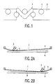
- Fig. 1 is a schematic cross-sectional view of a part of a screen-printing screen from which the photopolymer layer has been partly removed.
- Fig. 2A and Fig. 2B schematically show the screen printing process in which the squeegee is passed over the screen to spread the paste, so that after removal of the squeegee paste remains on the substrate at the location of the apertures in the screen.
- Fig. 3A is a schematic cross-sectional view of a stencil.
- Fig. 3B is a schematic cross-sectional view of a stencil which is locally provided, on the side of the stencil facing away from the substrate during the printing process, with a reservoir above the holes.
- Fig. 4A is a schematic cross-sectional view of a part of a stencil with two layers.
- Fig. 4B is a schematic cross-sectional view of a stencil with three layers.
- Fig. 4C is a schematic plan view of a stencil whose pattern is in accordance with a closed form.
- Fig. 1 is a schematic cross-sectional view of a part of a screen-printing screen in which the wires of the woven screen and the photopolymer are referenced (1) and (2), respectively.
- Fig. 2A shows the position of the squeegee (3) on the screen (4). Said squeegee (3) spreads the paste (5), thereby exerting a pressure on the screen (4) so that said screen engages the substrate (6).
- An aperture in the screen (4) is indicated by reference numeral (7).
- Fig. 2B shows that after the paste-spreading squeegee (3) has passed over the aperture (7), a quantity of paste (8) is applied to the substrate (6) at the location of said aperture.
- Figs. 3A and 3B are schematic views of stencils.
- the stencil shown in Fig. 3B is locally provided with a recess (9) above the holes (10), so that less paste is provided at said location during the printing process.
- These stencils have the advantage that, unlike the screen-printing screen, problems regarding resolution are precluded. Gauze, which limits the resolution, is absent.
- Fig. 4A is a schematic, cross-sectional view of a stencil (8) with two layers.
- Fig. 4B is a schematic cross-sectional view of a stencil (19) with additional reservoirs (20) above the capillaries (16) (a stencil with three layers).
- the multilayer stencils for example:
- the advantage of the third embodiment is that by using a flexible layer the risk of running is reduced.
- the side of an ordinary stencil facing the substrate during the printing process can also be provided with a flexible layer.
- Thin lines printed in accordance with the invention are much less subject to deformation than the lines printed by means of the screen-printing process. It is also possible to utilize variable paste transfer, i.e. the locally desired quantity of paste can be provided. This is important, for example, when layers are applied to surfaces having recesses or holes. Finally, running can be precluded.
- the invention relates to providing fine tracks, for example conductive tracks, in a flat display device (such as plasma display or PALC display) by means of a stencil printing method.
- a stencil printing method use can be made of multilayer stencils enabling the quantity of printing paste passed to be varied locally.
Landscapes
- Engineering & Computer Science (AREA)
- Manufacturing & Machinery (AREA)
- Microelectronics & Electronic Packaging (AREA)
- Physics & Mathematics (AREA)
- General Physics & Mathematics (AREA)
- Printing Plates And Materials Therefor (AREA)
- Printing Methods (AREA)
- Manufacturing Of Printed Wiring (AREA)
- Screen Printers (AREA)
- Photosensitive Polymer And Photoresist Processing (AREA)
- Liquid Crystal (AREA)
- Gas-Filled Discharge Tubes (AREA)
Claims (8)
- Procédé pour appliquer des pistes sur un substrat (6) selon une configuration au moyen d'une technique d'impression qui fait usage pour l'impression d'un pochoir (18, 19) ayant des ouvertures (10) selon la configuration à appliquer sur le substrat, caractérisé en ce que des évidements (9) se situent au-dessus des ouvertures (10) présentes dans le pochoir (18, 19).
- Procédé selon la revendication 1, suivant lequel la configuration à appliquer sur le substrat (6) est formée dans le côté du pochoir (18, 19) situé vis-à-vis du substrat pendant le processus d'impression et ledit pochoir est pourvu de capillaires (16) qui sont en communication ouverte avec les évidements (9) étant situés au-dessus de ladite configuration.
- Procédé selon la revendication 2, caractérisé en ce que des réservoirs (20) se situent au-dessus des capillaires (16) et en ce qu'ils sont en communication ouverte avec lesdits capillaires.
- Procédé selon la revendication 1, 2 ou 3, caractérisé en ce que le pochoir (18, 19) est fabriqué entièrement à partir de métal.
- Procédé selon la revendication 2 ou 3, caractérisé en ce que le côté du pochoir (18, 19) situé à l'opposé du substrat (6) pendant le processus d'impression est fabriqué à partir de métal et en ce que le côté situé vis-à-vis du substrat pendant le processus d'impression est fabriqué à partir de matériau synthétique.
- Procédé selon la revendication 1, 2 ou 3, caractérisé en ce que le côté du pochoir (18, 19) situé vis-à-vis du substrat pendant le processus d'impression comporte une couche constituée d'un matériau flexible.
- Procédé selon l'une quelconque des revendications précédentes, caractérisé en ce que le procédé est mis en oeuvre pour appliquer des configurations de résist.
- Procédé selon la revendication 1, 2, 3, 4, 5 ou 6, caractérisé en ce que le procédé est mis en oeuvre pour appliquer des configurations constituées d'un matériau électroconducteur sur un substrat constitué d'un matériau électriquement isolant.
Priority Applications (1)
| Application Number | Priority Date | Filing Date | Title |
|---|---|---|---|
| EP97920900A EP0843840B1 (fr) | 1996-06-11 | 1997-05-23 | Creation de pistes sur des substrats plats au moyen d'un procede d'impression au pochoir |
Applications Claiming Priority (6)
| Application Number | Priority Date | Filing Date | Title |
|---|---|---|---|
| EP96201623 | 1996-06-11 | ||
| EP96201623 | 1996-06-11 | ||
| EP96201824 | 1996-07-01 | ||
| EP96201824 | 1996-07-01 | ||
| PCT/IB1997/000587 WO1997048020A1 (fr) | 1996-06-11 | 1997-05-23 | Creation de pistes sur des substrats plats au moyen d'un procede d'impression au pochoir |
| EP97920900A EP0843840B1 (fr) | 1996-06-11 | 1997-05-23 | Creation de pistes sur des substrats plats au moyen d'un procede d'impression au pochoir |
Publications (2)
| Publication Number | Publication Date |
|---|---|
| EP0843840A1 EP0843840A1 (fr) | 1998-05-27 |
| EP0843840B1 true EP0843840B1 (fr) | 2001-10-17 |
Family
ID=26142883
Family Applications (1)
| Application Number | Title | Priority Date | Filing Date |
|---|---|---|---|
| EP97920900A Expired - Lifetime EP0843840B1 (fr) | 1996-06-11 | 1997-05-23 | Creation de pistes sur des substrats plats au moyen d'un procede d'impression au pochoir |
Country Status (6)
| Country | Link |
|---|---|
| US (1) | US5888584A (fr) |
| EP (1) | EP0843840B1 (fr) |
| JP (1) | JPH11510754A (fr) |
| KR (1) | KR19990036273A (fr) |
| DE (1) | DE69707394T2 (fr) |
| WO (1) | WO1997048020A1 (fr) |
Families Citing this family (8)
| Publication number | Priority date | Publication date | Assignee | Title |
|---|---|---|---|---|
| GB2333742A (en) * | 1998-01-29 | 1999-08-04 | John Michael Lowe | Flexible screen suitable for use in screen printing and method of making same |
| US5878661A (en) * | 1998-07-13 | 1999-03-09 | Ford Motor Company | Self-shearing stencil |
| NL1012100C2 (nl) * | 1999-05-19 | 2000-11-21 | Stork Screens Bv | Werkwijze voor het vervaardigen van een rotatiezeefdrukvorm, alsmede toepassing daarvan. |
| BR0010624A (pt) * | 1999-05-19 | 2002-02-19 | Stork Screens Bv | Processo para fabricação de uma matriz de impressão, bem como método de impressão usando uma matriz de impressão assim fabricado |
| US6217989B1 (en) * | 1999-12-10 | 2001-04-17 | International Business Machines Corporation | Conductive line features for enhanced reliability of multi-layer ceramic substrates |
| US20060009409A1 (en) * | 2002-02-01 | 2006-01-12 | Woolf Tod M | Double-stranded oligonucleotides |
| TWI633819B (zh) * | 2011-12-23 | 2018-08-21 | 新加坡商Asm組合系統新加坡有限公司 | 用於將沈積物之圖案印刷於基板上之模板、以沈積物之圖案印刷基板之方法及製作發光裝置之方法 |
| US8973524B2 (en) * | 2012-11-27 | 2015-03-10 | Intermolecular, Inc. | Combinatorial spin deposition |
Family Cites Families (8)
| Publication number | Priority date | Publication date | Assignee | Title |
|---|---|---|---|---|
| JPS61113064A (ja) * | 1984-11-07 | 1986-05-30 | Mitsubishi Electric Corp | 印刷用マスク |
| US4636406A (en) * | 1984-12-31 | 1987-01-13 | Motorola, Inc. | Method and apparatus for dispensing solder paste |
| US4803110A (en) * | 1986-09-15 | 1989-02-07 | International Business Machines Corporation | Coated mask for photolithographic construction of electric circuits |
| US4961955A (en) * | 1988-12-20 | 1990-10-09 | Itt Corporation | Solder paste applicator for circuit boards |
| US5046415A (en) * | 1989-01-06 | 1991-09-10 | Motorola, Inc. | Composite stencil for screen printing |
| US4953460A (en) * | 1989-10-02 | 1990-09-04 | At&T Bell Laboratories | Method and apparatus for screen printing |
| US5361695A (en) * | 1991-07-08 | 1994-11-08 | Danippon Screen Mfg. Co., Ltd. | Screen printing plate for limiting the spread of ink on an object |
| US5359928A (en) * | 1992-03-12 | 1994-11-01 | Amtx, Inc. | Method for preparing and using a screen printing stencil having raised edges |
-
1997
- 1997-05-23 KR KR1019980700941A patent/KR19990036273A/ko not_active Ceased
- 1997-05-23 WO PCT/IB1997/000587 patent/WO1997048020A1/fr not_active Ceased
- 1997-05-23 JP JP10501386A patent/JPH11510754A/ja active Pending
- 1997-05-23 DE DE69707394T patent/DE69707394T2/de not_active Expired - Fee Related
- 1997-05-23 EP EP97920900A patent/EP0843840B1/fr not_active Expired - Lifetime
- 1997-06-05 US US08/870,056 patent/US5888584A/en not_active Expired - Fee Related
Also Published As
| Publication number | Publication date |
|---|---|
| EP0843840A1 (fr) | 1998-05-27 |
| DE69707394D1 (de) | 2001-11-22 |
| US5888584A (en) | 1999-03-30 |
| KR19990036273A (ko) | 1999-05-25 |
| WO1997048020A1 (fr) | 1997-12-18 |
| DE69707394T2 (de) | 2002-07-11 |
| JPH11510754A (ja) | 1999-09-21 |
Similar Documents
| Publication | Publication Date | Title |
|---|---|---|
| US4324815A (en) | Screen-printing mask and method | |
| US5373786A (en) | Metal mask plate for screen printing | |
| US4242401A (en) | Screen-printing mask | |
| US5046415A (en) | Composite stencil for screen printing | |
| EP0285850B1 (fr) | Méthode de sérigraphie pour la fabrication des lignes d'une largeur et d'une hauteur uniforme de circuit imprimé | |
| US5927193A (en) | Process for via fill | |
| US4481881A (en) | Hot melt screen printing machine | |
| JP3557618B2 (ja) | 基盤に粘性物質を点ベースの皮膜として堆積させ配分する方法、シルクスクリーンステンシルを製造する方法、電子部品を基盤に搭載するための粘性物質を点状に堆積および配分する方法 | |
| EP0843840B1 (fr) | Creation de pistes sur des substrats plats au moyen d'un procede d'impression au pochoir | |
| GB2030007A (en) | Printed circuit board manufacture | |
| US4604298A (en) | Finger line screen printing method and apparatus | |
| CA1174506A (fr) | Methode de production d'un cliche de serigraphie rotative a reliefs | |
| JP2023138827A (ja) | スクリーンマスク、スクリーンマスクの製造方法及び印刷物の製造方法 | |
| JPH06202314A (ja) | 印刷版とその製造方法および印刷版を用いたパターンの形成方法 | |
| CN103042818B (zh) | 网版结构 | |
| US5807610A (en) | Flex tab thick film metal mask to deposit coating material | |
| JP4720002B2 (ja) | スクリーン印刷版及びその製造方法 | |
| US5456942A (en) | Method for fabricating a circuit element through a substrate | |
| EP0843886A1 (fr) | Creation d'elements colores sur des substrats au moyen d'un procede de serigraphie ou d'impression au pochoir | |
| JP2016219508A (ja) | 電子デバイスの製造方法および電子デバイス | |
| JP4001973B2 (ja) | メッシュ一体型のメタルマスクの製造方法 | |
| WO2000048845A1 (fr) | Stencil ameliore | |
| JPH02112993A (ja) | 厚膜回路基板の製造方法及び製造用メッシュマスク | |
| JPS5917555B2 (ja) | 導電パタ−ン膜の形成方法 | |
| JPH09174809A (ja) | スクリーン印刷用スキージ |
Legal Events
| Date | Code | Title | Description |
|---|---|---|---|
| PUAI | Public reference made under article 153(3) epc to a published international application that has entered the european phase |
Free format text: ORIGINAL CODE: 0009012 |
|
| AK | Designated contracting states |
Kind code of ref document: A1 Designated state(s): DE FR GB |
|
| RAP3 | Party data changed (applicant data changed or rights of an application transferred) |
Owner name: KONINKLIJKE PHILIPS ELECTRONICS N.V. |
|
| 17P | Request for examination filed |
Effective date: 19980618 |
|
| 17Q | First examination report despatched |
Effective date: 19990707 |
|
| RIC1 | Information provided on ipc code assigned before grant |
Free format text: 7G 03F 7/12 A, 7B 41C 1/14 B |
|
| GRAG | Despatch of communication of intention to grant |
Free format text: ORIGINAL CODE: EPIDOS AGRA |
|
| GRAG | Despatch of communication of intention to grant |
Free format text: ORIGINAL CODE: EPIDOS AGRA |
|
| GRAH | Despatch of communication of intention to grant a patent |
Free format text: ORIGINAL CODE: EPIDOS IGRA |
|
| GRAH | Despatch of communication of intention to grant a patent |
Free format text: ORIGINAL CODE: EPIDOS IGRA |
|
| GRAA | (expected) grant |
Free format text: ORIGINAL CODE: 0009210 |
|
| AK | Designated contracting states |
Kind code of ref document: B1 Designated state(s): DE FR GB |
|
| REF | Corresponds to: |
Ref document number: 69707394 Country of ref document: DE Date of ref document: 20011122 |
|
| REG | Reference to a national code |
Ref country code: GB Ref legal event code: IF02 |
|
| ET | Fr: translation filed | ||
| PLBE | No opposition filed within time limit |
Free format text: ORIGINAL CODE: 0009261 |
|
| STAA | Information on the status of an ep patent application or granted ep patent |
Free format text: STATUS: NO OPPOSITION FILED WITHIN TIME LIMIT |
|
| 26N | No opposition filed | ||
| REG | Reference to a national code |
Ref country code: FR Ref legal event code: D6 |
|
| REG | Reference to a national code |
Ref country code: GB Ref legal event code: 746 Effective date: 20021107 |
|
| PGFP | Annual fee paid to national office [announced via postgrant information from national office to epo] |
Ref country code: FR Payment date: 20030526 Year of fee payment: 7 |
|
| PGFP | Annual fee paid to national office [announced via postgrant information from national office to epo] |
Ref country code: GB Payment date: 20030529 Year of fee payment: 7 |
|
| PGFP | Annual fee paid to national office [announced via postgrant information from national office to epo] |
Ref country code: DE Payment date: 20030715 Year of fee payment: 7 |
|
| PG25 | Lapsed in a contracting state [announced via postgrant information from national office to epo] |
Ref country code: GB Free format text: LAPSE BECAUSE OF NON-PAYMENT OF DUE FEES Effective date: 20040523 |
|
| PG25 | Lapsed in a contracting state [announced via postgrant information from national office to epo] |
Ref country code: DE Free format text: LAPSE BECAUSE OF NON-PAYMENT OF DUE FEES Effective date: 20041201 |
|
| GBPC | Gb: european patent ceased through non-payment of renewal fee |
Effective date: 20040523 |
|
| PG25 | Lapsed in a contracting state [announced via postgrant information from national office to epo] |
Ref country code: FR Free format text: LAPSE BECAUSE OF NON-PAYMENT OF DUE FEES Effective date: 20050131 |
|
| REG | Reference to a national code |
Ref country code: FR Ref legal event code: ST |