EP0843909B1 - Dispositif de commande d'une source laser a plusieurs modules laser pour optimiser energetiquement et spatialement le traitement de surface par laser - Google Patents
Dispositif de commande d'une source laser a plusieurs modules laser pour optimiser energetiquement et spatialement le traitement de surface par laser Download PDFInfo
- Publication number
- EP0843909B1 EP0843909B1 EP96924950A EP96924950A EP0843909B1 EP 0843909 B1 EP0843909 B1 EP 0843909B1 EP 96924950 A EP96924950 A EP 96924950A EP 96924950 A EP96924950 A EP 96924950A EP 0843909 B1 EP0843909 B1 EP 0843909B1
- Authority
- EP
- European Patent Office
- Prior art keywords
- laser
- laser beam
- energy
- resulting
- unit
- Prior art date
- Legal status (The legal status is an assumption and is not a legal conclusion. Google has not performed a legal analysis and makes no representation as to the accuracy of the status listed.)
- Expired - Lifetime
Links
- 238000005542 laser surface treatment Methods 0.000 title claims abstract description 9
- 238000009826 distribution Methods 0.000 claims abstract description 10
- 230000008878 coupling Effects 0.000 claims abstract description 7
- 238000010168 coupling process Methods 0.000 claims abstract description 7
- 238000005859 coupling reaction Methods 0.000 claims abstract description 7
- 238000004381 surface treatment Methods 0.000 claims abstract description 4
- 230000003287 optical effect Effects 0.000 claims description 15
- 229910021417 amorphous silicon Inorganic materials 0.000 claims description 12
- 238000011282 treatment Methods 0.000 claims description 9
- 238000000137 annealing Methods 0.000 claims description 5
- 239000000463 material Substances 0.000 claims description 2
- 238000000265 homogenisation Methods 0.000 claims 1
- 239000004065 semiconductor Substances 0.000 claims 1
- 101100227197 Arabidopsis thaliana FLA2 gene Proteins 0.000 description 9
- 230000004927 fusion Effects 0.000 description 9
- 101100012983 Arabidopsis thaliana FLA1 gene Proteins 0.000 description 7
- 101100227198 Campylobacter jejuni flaA gene Proteins 0.000 description 7
- 239000000758 substrate Substances 0.000 description 7
- XUIMIQQOPSSXEZ-UHFFFAOYSA-N Silicon Chemical compound [Si] XUIMIQQOPSSXEZ-UHFFFAOYSA-N 0.000 description 6
- 229910052710 silicon Inorganic materials 0.000 description 6
- 239000010703 silicon Substances 0.000 description 6
- 238000010521 absorption reaction Methods 0.000 description 4
- 230000007246 mechanism Effects 0.000 description 4
- 238000000034 method Methods 0.000 description 4
- 229910021420 polycrystalline silicon Inorganic materials 0.000 description 4
- 229920005591 polysilicon Polymers 0.000 description 4
- 102100023882 Endoribonuclease ZC3H12A Human genes 0.000 description 3
- 101710112715 Endoribonuclease ZC3H12A Proteins 0.000 description 3
- 241000861223 Issus Species 0.000 description 3
- 230000008901 benefit Effects 0.000 description 3
- 238000010438 heat treatment Methods 0.000 description 3
- QGVYYLZOAMMKAH-UHFFFAOYSA-N pegnivacogin Chemical compound COCCOC(=O)NCCCCC(NC(=O)OCCOC)C(=O)NCCCCCCOP(=O)(O)O QGVYYLZOAMMKAH-UHFFFAOYSA-N 0.000 description 3
- PEDCQBHIVMGVHV-UHFFFAOYSA-N Glycerine Chemical compound OCC(O)CO PEDCQBHIVMGVHV-UHFFFAOYSA-N 0.000 description 2
- 108700012361 REG2 Proteins 0.000 description 2
- 101150108637 REG2 gene Proteins 0.000 description 2
- 108091058543 REG3 Proteins 0.000 description 2
- 101100120298 Rattus norvegicus Flot1 gene Proteins 0.000 description 2
- 101100412403 Rattus norvegicus Reg3b gene Proteins 0.000 description 2
- 102100027336 Regenerating islet-derived protein 3-alpha Human genes 0.000 description 2
- 239000013078 crystal Substances 0.000 description 2
- 230000005284 excitation Effects 0.000 description 2
- 239000011521 glass Substances 0.000 description 2
- 238000009434 installation Methods 0.000 description 2
- 239000004973 liquid crystal related substance Substances 0.000 description 2
- 238000004519 manufacturing process Methods 0.000 description 2
- 239000011159 matrix material Substances 0.000 description 2
- 238000002844 melting Methods 0.000 description 2
- 230000008018 melting Effects 0.000 description 2
- 101001006782 Homo sapiens Kinesin-associated protein 3 Proteins 0.000 description 1
- 102100027930 Kinesin-associated protein 3 Human genes 0.000 description 1
- 230000004075 alteration Effects 0.000 description 1
- 238000004140 cleaning Methods 0.000 description 1
- 238000001816 cooling Methods 0.000 description 1
- 238000002425 crystallisation Methods 0.000 description 1
- 230000008025 crystallization Effects 0.000 description 1
- 238000005520 cutting process Methods 0.000 description 1
- 230000001419 dependent effect Effects 0.000 description 1
- 238000006073 displacement reaction Methods 0.000 description 1
- 230000000694 effects Effects 0.000 description 1
- 230000002349 favourable effect Effects 0.000 description 1
- 238000005224 laser annealing Methods 0.000 description 1
- 238000004093 laser heating Methods 0.000 description 1
- 239000007788 liquid Substances 0.000 description 1
- 238000004377 microelectronic Methods 0.000 description 1
- 238000011369 optimal treatment Methods 0.000 description 1
- 238000005554 pickling Methods 0.000 description 1
- 238000005498 polishing Methods 0.000 description 1
- 230000008569 process Effects 0.000 description 1
- 238000005086 pumping Methods 0.000 description 1
- 238000001953 recrystallisation Methods 0.000 description 1
- 230000000630 rising effect Effects 0.000 description 1
- 238000007711 solidification Methods 0.000 description 1
- 230000008023 solidification Effects 0.000 description 1
- 230000002123 temporal effect Effects 0.000 description 1
- 239000010409 thin film Substances 0.000 description 1
Images



Classifications
-
- H—ELECTRICITY
- H01—ELECTRIC ELEMENTS
- H01S—DEVICES USING THE PROCESS OF LIGHT AMPLIFICATION BY STIMULATED EMISSION OF RADIATION [LASER] TO AMPLIFY OR GENERATE LIGHT; DEVICES USING STIMULATED EMISSION OF ELECTROMAGNETIC RADIATION IN WAVE RANGES OTHER THAN OPTICAL
- H01S3/00—Lasers, i.e. devices using stimulated emission of electromagnetic radiation in the infrared, visible or ultraviolet wave range
- H01S3/23—Arrangements of two or more lasers not provided for in groups H01S3/02 - H01S3/22, e.g. tandem arrangements of separate active media
-
- H—ELECTRICITY
- H01—ELECTRIC ELEMENTS
- H01S—DEVICES USING THE PROCESS OF LIGHT AMPLIFICATION BY STIMULATED EMISSION OF RADIATION [LASER] TO AMPLIFY OR GENERATE LIGHT; DEVICES USING STIMULATED EMISSION OF ELECTROMAGNETIC RADIATION IN WAVE RANGES OTHER THAN OPTICAL
- H01S3/00—Lasers, i.e. devices using stimulated emission of electromagnetic radiation in the infrared, visible or ultraviolet wave range
- H01S3/23—Arrangements of two or more lasers not provided for in groups H01S3/02 - H01S3/22, e.g. tandem arrangements of separate active media
- H01S3/2308—Amplifier arrangements, e.g. MOPA
- H01S3/2316—Cascaded amplifiers
-
- B—PERFORMING OPERATIONS; TRANSPORTING
- B23—MACHINE TOOLS; METAL-WORKING NOT OTHERWISE PROVIDED FOR
- B23K—SOLDERING OR UNSOLDERING; WELDING; CLADDING OR PLATING BY SOLDERING OR WELDING; CUTTING BY APPLYING HEAT LOCALLY, e.g. FLAME CUTTING; WORKING BY LASER BEAM
- B23K26/00—Working by laser beam, e.g. welding, cutting or boring
- B23K26/02—Positioning or observing the workpiece, e.g. with respect to the point of impact; Aligning, aiming or focusing the laser beam
- B23K26/06—Shaping the laser beam, e.g. by masks or multi-focusing
- B23K26/064—Shaping the laser beam, e.g. by masks or multi-focusing by means of optical elements, e.g. lenses, mirrors or prisms
- B23K26/066—Shaping the laser beam, e.g. by masks or multi-focusing by means of optical elements, e.g. lenses, mirrors or prisms by using masks
-
- H—ELECTRICITY
- H01—ELECTRIC ELEMENTS
- H01S—DEVICES USING THE PROCESS OF LIGHT AMPLIFICATION BY STIMULATED EMISSION OF RADIATION [LASER] TO AMPLIFY OR GENERATE LIGHT; DEVICES USING STIMULATED EMISSION OF ELECTROMAGNETIC RADIATION IN WAVE RANGES OTHER THAN OPTICAL
- H01S3/00—Lasers, i.e. devices using stimulated emission of electromagnetic radiation in the infrared, visible or ultraviolet wave range
- H01S3/23—Arrangements of two or more lasers not provided for in groups H01S3/02 - H01S3/22, e.g. tandem arrangements of separate active media
- H01S3/2383—Parallel arrangements
Definitions
- the present invention relates to the control of a laser source with several laser modules to optimize energy and spatially laser surface treatment.
- laser amorphous silicon annealing excimer is to very quickly raise the temperature of the layer of amorphous silicon until fusion to obtain crystallization in the form of a polysilicon. Fusion of the silicon layer must not disturb too much the standard glass substrate.
- the heating effect is due to absorption optical laser beam by a thin layer of silicon amorphous, for example on a thickness less than 30nm.
- Annealing of amorphous silicon by excimer laser requires excellent knowledge of structural features of the sample to be treated, as described at least in part in the Patent Application entitled “Device and laser surface treatment control method ", filed in France by the Claimant on August 11, 1995, under the No 95 09778.
- laser heating must be efficient because it strongly influences the thermal evolution of the sample, especially at the level of the fusion of the layer of silicon which must be total and at the level of the fusion of the substrate that should be avoided.
- the rate of cooling and solidification of the silicon layer should be relatively slow because it determines the size of the polysilicon grains present in the layer after annealing, the crystals of large are the most favorable for optimal operation, for certain micro-electronic devices based on silicon.
- Document DE-A-4009859 discloses a device for controlling a laser source according to the preamble of claim 1.
- the present invention provides a solution to this problem.
- a source control device laser comprising at least two laser modules as well as coupling means suitable for coupling the laser beams from each module to deliver a laser beam resulting intended for the treatment of a surface.
- resulting laser beam means a beam made up of a plurality of initial laser beams.
- the time profile of the power of the resulting laser beam includes a steep rising front to improve the heating efficiency, a level substantially dish corresponding to a depth of treatment, chosen in order to obtain a total fusion of the layer of amorphous silicon at said depth, while avoiding the melting of the substrate and a soft falling front to favor recrystallization.
- AMLCD Active Matrix Liquid Cristal Display
- TFT Polysilicon Thin Film Transistor
- This technique consists in exploiting absorption particularly strong silicon in the ultraviolet, while the substrate glass is completely transparent to the same wavelengths.
- a high power pulsed laser beam allows to selectively raise the temperature of the layer of amorphous silicon until fusion, without affecting the substrate.
- the process has the advantage of being able to be very fast (the duration average of a pulse from an excimer laser at 308 nm is only 150 ns).
- a laser excimer at high power for example a laser excimer at X-ray re-ionization providing effective power 1 kW (i.e. 10 d x 100 Hz or 13 d x 80 Hz).
- This type of laser advantageously makes it possible to obtain a beam high power laser, pulsed with repetition rate relatively low, which allows processing on a large area, even up to the entirety of each panel in a single laser pulse.
- the device implementing the method annealing device includes an LA laser source having a power supply (not shown) and a plurality of laser modules excimer individualized in LA1 to LA3.
- the laser modules, high power, are positioned and interconnected so to produce a single very high power laser beam, for example 45 J.
- one of the mirrors is maximum reflection. This mirror is designated by the reference RM. Diametrically opposite to it, the RT mirror is semi-reflecting.
- the RM mirror can be a simple mirror with maximum reflection.
- Figures 1 and 2 it can be made under the shape of a cube corner, a dihedral dihedral or a dihedral whose function, in addition to maximum reflection, is to symmetricize the energy and spatial distribution of laser beam with respect to the optical axis of said cube corner or the like.
- This laser beam thus made symmetrical can constitute a significant advantage in the distribution spatial and energetic of the resulting laser beam that we will describe in more detail below.
- LA2 and LA3 laser mounted in series. These amplifier modules do not have RM and RT mirrors. These modules amplify the beam receive.
- the reflection of the oscillator's RM mirror is maximum at wavelength of the excimer laser, here 308 nm.
- the mirror of RT output of oscillator LA1 has a reflection coefficient in the range of 4 to 40%.
- the dimensions of the laser modules LA1 to LA3 are approximately as follows.
- Figure 2 One solution (Figure 2) is to use mirrors deflection and focusing lenses to reduce bulk from such a laser source.
- Figure 2 differs from Figure 1 by using return mirrors M1, M2, M3 and M4 to route the resulting laser beam on the CIB target.
- Focusing lenses L1 and L2 are also arranged to focus the wave between the source LA1 and LA2 for the lens L1, and between source LA2 and source LA3 for the L2 lens.
- REG1 adjustment mechanisms between the source LA1 and LA2, as well as between source LA2 and LA3 are provided to adjust the distance between these two modules by function of the desired laser time profile which will be described in more detail below.
- the choice of the lengths of the different modules as well as distances between the different modules connected in series allows to adjust the energy delivered by the resulting FLAR laser beam to be applied to the sample to be processed at the CIB level.
- the adjustment mechanisms REG1 and REG2 are means suitable for moving the optical elements M1, L1, M2 and M3, L2, M4 along the optical axis of the laser beam. They allow by translation parallel to the axes of the beams incidents and emerging to vary the length of the journey optics between LA1 and LA2 for REG1, between LA2 and LA3 for REG2.
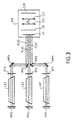
- the laser modules can be put in parallel. So, we find the three laser modules LA1 to LA3 described above. These play all, here, the role of oscillator with each a mirror maximum reflector RM and a partial reflector mirror RT.
- coupling means constituted by return mirrors MP1, MP2, MP3 and MP4 allow coupling of the pulse beams FLA1, FLA2 and FL3 laser from each oscillator towards the CIB target plan.
- an HO homogenizer is provided to homogenize the laser beams from each module.
- the homogenizer is that described in the Request filed by the Applicant for "Optical device to homogenize a laser beam "on the same day as the this Patent Application.
- the HO homogenizer device comprises two collection lenses LC1 and LC2 mobile in translation along the optical axis, the distance d between the two lenses being chosen to adapt according to the invention the size and the energy of the resulting FLAR laser beam on application chosen.
- the combination of collection lenses LC1 and LC2 is calculated to minimize aberrations possible optics of the laser source coupled with the homogenizers and to improve the characteristics energy per unit area (constancy of the fluence of the resulting laser beam).
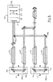
- the LA1 module plays the role here amplifier instead of playing the role of oscillator like described with reference to Figure 3.
- the LA2 and LA1 modules are here in series to deliver a laser beam resulting pulse FLA2 intended to be routed to the CIB target plan.
- the HO homogenizer is designed to homogenize the beams laser from the LA3 module delivering the FLA3 laser beam as well as the FLA2 laser beam from LA2 and LA1 modules put in series.
- a REG3 adjustment mechanism is provided between the LA2 module and LA1 module to adjust the distance between the two modules.
- M4, M5, M6 and M7 deflection mirrors carry the FLA2 laser beam from LA2 module to LA1 module then the laser beam FLA1 towards the target CIB.
- a focusing lens L3 is advantageously associated REG3 adjustment mechanism to focus the laser beam depending on the displacement of the optical elements.
- FIG. 5 a laser source with four has been represented. laser modules. Such an installation is symmetrical. She is distinguishes from that described with reference to FIG. 4 by the includes an additional laser amplifier module LA4 connected in series with the LA3 oscillator laser module in Figure 4.
- each panel has dimensions of the order of 550 x 650 mm.
- the resulting laser beam has a dimension adapted to the size of the panels to be treated.
- FIG. 6A two time profiles of the energy delivered by two laser beams are shown, each coming from a laser module.
- the total energy of each beam is 0.8 J / cm 2 .
- the energy in mW / cm 2 is represented on the ordinate axis while the time in ns is represented on the abscissa axis.
- FIG. 6B the thickness of the layer is shown melted as a function of time by the two laser beams FLA1 and FLA2 described with reference to FIG. 6A.
- the laser beam FLA2 comprises a front of rise in power 2A steeper than that 1A of the beam FLA1 laser.
- the laser beam FLA1 includes a power step 1B significantly flatter at a depth of 50 nm, than that 2B of the laser beam FLA2.
- the depth of 50 nm corresponds to the thickness of the layer of amorphous silicon to be annealed by laser.
- the laser beam FLA1 comprises a falling edge in power 1C significantly softer than that 2C of the laser beam FLA2.
- the time profile of the resulting laser beam desired includes a substantially ramp-up front steep to improve the heating efficiency, a substantially flat power level at a depth of chosen treatment to obtain a total fusion of the layer of amorphous silicon at said depth while avoiding the melting of the substrate, and a falling front in noticeably soft power to promote the growth of crystals.
- the laser beams coming from each laser module to obtain a resulting laser beam with such a time profile.
- the adjustment means include means trigger to trigger the oscillator modules laser with a chosen time offset.
- Another solution according to the invention consists in adjusting the module lengths as well as the distances between different modules in order to obtain a resulting laser beam presenting the temporal profile adapted to the treatment of area. For example, a profile as described above.
- Another solution according to the invention consists in varying the energy used by each individual laser module to that the resulting laser beam represents the chosen profile.
- the variation means can be optical means (diaphragms) and / or mechanical.
- Another solution according to the invention consists in adjusting the distance d between the two focusing lenses of the homogenizer described above.
Landscapes
- Physics & Mathematics (AREA)
- Optics & Photonics (AREA)
- Electromagnetism (AREA)
- Engineering & Computer Science (AREA)
- Plasma & Fusion (AREA)
- Mechanical Engineering (AREA)
- Recrystallisation Techniques (AREA)
- Laser Beam Processing (AREA)
- Lasers (AREA)
Description
- la figure 1 représente schématiquement une source laser comprenant trois modules laser montés en série;
- la figure 2 représente schématiquement une source laser comprenant trois modules laser montés en série avec des miroirs de renvoi et des lentilles de focalisation;
- la figure 3 représente schématiquement une source laser comprenant trois modules laser amplificateurs montés en parallèle;
- la figure 4 représente schématiquement une source laser à deux modules laser oscillateurs montés en parallèle, l'un des oscillateurs étant associé en outre à un module amplificateur;
- la figure 5 représente schématiquement une source laser à deux modules laser oscillateurs montés en parallèle, chaque module oscillateur étant en outre associé à un module amplificateur;
- la figure 6A représente schématiquement les profils temporels de deux faisceaux laser issus chacun d'un module; et
- la figure 6B représente schématiquement la profondeur de fusion en fonction du temps de traitement pour les deux profils temporels de laser de la figure 6A.
- un matériau ou milieu laser actif capable d'amplifier une onde incidente;
- des moyens de pompage optique (non représentés) qui apportent au milieu de l'énergie propre à peupler l'un au moins de ses niveaux d'excitation, afin de réaliser une inversion de population dans le milieu actif; et
- un résonateur optique, composé de deux miroirs disposés face à face, qui accumule l'émission induite concentrée sur quelques modes du résonateur.
- une pluralité de m.n lentilles frontales LF convergentes, jointives, disposées en m lignes et n colonnes, perpendiculairement à la direction de propagation des faisceaux laser issus de chaque module laser, et propres à découper les faisceaux laser à traiter en m.n faisceaux laser ayant chacun une section transversale sensiblement uniforme, et une répartition énergétique sensiblement homogène, et
- au moins une lentille de collection LC, convergente, disposée perpendiculairement à la direction de propagation des faisceaux laser à traiter, en aval des lentilles frontales LF selon le sens du cheminement du faisceau laser, ladite lentille de collection étant propre à focaliser dans un plan choisi CIB les faisceaux issus des lentilles frontales.
Claims (13)
- Dispositif de commande d'une source laser, comprenant au moins deux modules laser (LA1, LA2) ainsi que des moyens de couplage propres à coupler les faisceaux laser issus de chaque module pour délivrer un faisceau laser résultant destiné au traitement d'une surface,
ledit dispositif étant caractérisé en ce qu'il comprend en outre, en combinaison avec le traitement de surface par laser:des moyens d'ajustement (REG) propres à ajuster les caractéristiques des faisceaux laser issus de chaque module pour obtenir un faisceau laser résultant avec un profil temporel de puissance énergétique adapté de façon optimale audit traitement de surface laser, etdes moyens homogénéiseurs (HO) propres à homogénéiser spatialement la répartition énergétique dudit faisceau laser résultant, ce qui permet d'adapter, en combinaison, la répartition spatiale et énergétique dudit faisceau laser résultant au traitement de surface choisi. - Dispositif selon la revendication 1, caractérisé en ce que les moyens d'ajustement sont propres à obtenir un profil temporel de la puissance énergétique du faisceau laser résultant avec un front de montée en puissance sensiblement raide, un palier en puissance sensiblement plat à une profondeur de traitement choisie et un front de descente en puissance sensiblement doux.
- Dispositif selon la revendication 1 ou la revendication 2, caractérisé en ce que les moyens d'ajustement comprennent des moyens propres à faire varier optiquement et/ou mécaniquement l'énergie délivrée par chaque module laser.
- Dispositif selon la revendication 1 ou la revendication 2, caractérisé en ce que les moyens d'ajustement comprennent des moyens de réglage propres à régler les caractéristiques optiques et/ou géométriques des faisceaux laser issus de chaque module laser.
- Dispositif selon la revendication 1, caractérisé en ce que la source laser comprend au moins un module amplificateur laser et un module oscillateur montés en série.
- Dispositif selon la revendication 5, caractérisé en ce que le module oscillateur laser comprend un miroir à réflexion totale (RM) agencé en coin de cube ou analogue pour symétriser le faisceau laser par rapport à l'axe optique dudit faisceau laser, et contribuer à l'homogénéisation du faisceau laser résultant.
- Dispositif selon la revendication 5, caractérisé en ce que les moyens d'ajustement comprennent des moyens de réglage (REG) propres à régler la longueur des modules laser ainsi que la distance entre les modules amplificateur et oscillateur en fonction de l'application choisie et de l'énergie laser à appliquer.
- Dispositif selon la revendication 5, caractérisé en ce que les moyens d'ajustement comprennent des moyens de déclenchement propres à déclencher les deux modules oscillateurs laser avec un décalage temporel choisi.
- Dispositif selon la revendication 1, caractérisé en ce la source laser comprend au moins deux modules oscillateurs laser montés en parallèle.
- Dispositif selon la revendication 9, caractérisé en ce les moyens d'ajustement comprennent des moyens de déclenchement propres à déclencher les deux modules oscillateurs laser avec un décalage temporel choisi.
- Dispositif selon la revendication 1, caractérisé en ce que le dispositif optique homogénéiseur de faisceau laser (HO) comprend :une pluralité de m.n lentilles frontales (LF) convergentes, jointives, disposées en m lignes et n colonnes, perpendiculairement à la direction de propagation des faisceaux laser issus de chaque module laser, et propres à découper les faisceaux laser à traiter en p.q faisceaux laser ayant chacun une section transversale sensiblement uniforme, et une répartition énergétique sensiblement homogène, p.q étant un sous-multiple de m.n,au moins une lentille de collection (LC), convergente, disposée perpendiculairement à la direction de propagation des faisceaux laser à traiter, en aval des lentilles frontales selon le sens du cheminement du faisceau laser, ladite lentille de collection étant propre à focaliser dans un plan choisi (CIB) les faisceaux issus des lentilles frontales.
- Dispositif selon la revendication 11, caractérisé en ce qu'il comprend deux lentilles de collection (LC1 et LC2) mobiles en translation selon l'axe optique, la distance (d) entre les deux lentilles étant choisie pour adapter la taille et l'énergie du faisceau laser résultant à l'application choisie et la combinaison desdites lentilles de collection (LC1 et LC2) étant susceptible d'être calculée pour minimiser les aberrations optiques de la source laser couplée avec les moyens homogénéiseurs et pour améliorer les caractéristiques énergétiques par unité de surface du faisceau laser résultant.
- Dispositif selon l'une des revendications 1 à 12, caractérisé en ce que le traitement de surface est un recuit d'un matériau semi-conducteur du type silicium amorphe.
Applications Claiming Priority (3)
| Application Number | Priority Date | Filing Date | Title |
|---|---|---|---|
| FR9509780A FR2737814B1 (fr) | 1995-08-11 | 1995-08-11 | Procede et dispositif de commande d'une source laser a plusieurs modules laser pour optimiser le traitement de surface par laser |
| FR9509780 | 1995-08-11 | ||
| PCT/FR1996/001060 WO1997007578A1 (fr) | 1995-08-11 | 1996-07-05 | Dispositif de commande d'une source laser a plusieurs modules laser pour optimiser energetiquement et spatialement le traitement de surface par laser |
Publications (2)
| Publication Number | Publication Date |
|---|---|
| EP0843909A1 EP0843909A1 (fr) | 1998-05-27 |
| EP0843909B1 true EP0843909B1 (fr) | 1999-05-26 |
Family
ID=9481900
Family Applications (1)
| Application Number | Title | Priority Date | Filing Date |
|---|---|---|---|
| EP96924950A Expired - Lifetime EP0843909B1 (fr) | 1995-08-11 | 1996-07-05 | Dispositif de commande d'une source laser a plusieurs modules laser pour optimiser energetiquement et spatialement le traitement de surface par laser |
Country Status (9)
| Country | Link |
|---|---|
| US (1) | US6014401A (fr) |
| EP (1) | EP0843909B1 (fr) |
| JP (1) | JP4169366B2 (fr) |
| KR (1) | KR100416246B1 (fr) |
| AT (1) | ATE180601T1 (fr) |
| CA (1) | CA2225152C (fr) |
| DE (1) | DE69602603T2 (fr) |
| FR (1) | FR2737814B1 (fr) |
| WO (1) | WO1997007578A1 (fr) |
Families Citing this family (17)
| Publication number | Priority date | Publication date | Assignee | Title |
|---|---|---|---|---|
| FR2737786B1 (fr) * | 1995-08-11 | 1997-09-12 | Soc D Production Et De Rech Ap | Dispositif optique pour homogeneiser un faisceau laser |
| FR2737806B1 (fr) * | 1995-08-11 | 1997-09-12 | Soc D Production Et De Rech Ap | Dispositif et procede de traitement de surface par laser |
| JP2002289397A (ja) * | 2001-03-23 | 2002-10-04 | Takayasu Mochizuki | レーザプラズマ発生方法およびそのシステム |
| JP2003059858A (ja) * | 2001-08-09 | 2003-02-28 | Sony Corp | レーザアニール装置及び薄膜トランジスタの製造方法 |
| US7097709B2 (en) * | 2002-11-27 | 2006-08-29 | Mitsubishi Denki Kabushiki Kaisha | Laser annealing apparatus |
| SG129265A1 (en) * | 2002-11-29 | 2007-02-26 | Semiconductor Energy Lab | Laser irradiation apparatus, laser irradiation method, and method for manufacturing a semiconductor device |
| US7304005B2 (en) * | 2003-03-17 | 2007-12-04 | Semiconductor Energy Laboratory Co., Ltd. | Laser irradiation apparatus, laser irradiation method, and method for manufacturing a semiconductor device |
| JP2007515774A (ja) * | 2003-07-30 | 2007-06-14 | ティーシーゼット ピーティーイー リミテッド | 超高エネルギ高安定性ガス放電レーザ表面処理システム |
| DE102004001276A1 (de) * | 2004-01-08 | 2005-08-04 | Mtu Aero Engines Gmbh | Verfahren zur Erwärmung von Bauteilen |
| US20070012665A1 (en) * | 2005-07-12 | 2007-01-18 | Hewlett-Packard Development Company Lp | Laser ablation |
| CN102203943B (zh) * | 2008-10-29 | 2013-07-31 | 欧瑞康太阳能股份公司(特吕巴赫) | 通过多激光束照射将在基板上形成的半导体膜划分成多个区域的方法 |
| US8509272B2 (en) | 2009-06-10 | 2013-08-13 | Lee Laser, Inc. | Laser beam combining and power scaling device |
| US9277634B2 (en) | 2013-01-17 | 2016-03-01 | Kla-Tencor Corporation | Apparatus and method for multiplexed multiple discharge plasma produced sources |
| WO2016006099A1 (fr) * | 2014-07-11 | 2016-01-14 | ギガフォトン株式会社 | Système laser |
| CN108292595B (zh) | 2015-12-25 | 2022-09-16 | 极光先进雷射株式会社 | 激光照射装置 |
| WO2019012642A1 (fr) * | 2017-07-13 | 2019-01-17 | ギガフォトン株式会社 | Système laser |
| KR102324610B1 (ko) * | 2019-12-26 | 2021-11-09 | 세메스 주식회사 | 기판 가열 유닛, 기판 처리 장치 및 기판 처리 방법 |
Family Cites Families (16)
| Publication number | Priority date | Publication date | Assignee | Title |
|---|---|---|---|---|
| US4649351A (en) * | 1984-10-19 | 1987-03-10 | Massachusetts Institute Of Technology | Apparatus and method for coherently adding laser beams |
| US4648092A (en) * | 1985-09-25 | 1987-03-03 | Rockwell International Corporation | Phase coupling multiple lasers |
| EP0308512B1 (fr) * | 1987-02-24 | 1994-06-22 | Nippon Steel Corporation | Appareil pour le matage de rouleaux par un faisceau laser a impulsions |
| JPH01302881A (ja) * | 1988-05-31 | 1989-12-06 | Yoshiaki Arata | 大出力エキシマレーザービーム造出法 |
| US5253110A (en) * | 1988-12-22 | 1993-10-12 | Nikon Corporation | Illumination optical arrangement |
| DE4009859A1 (de) * | 1990-03-28 | 1991-10-02 | Fraunhofer Ges Forschung | Verfahren und vorrichtung zur erzeugung von laserstrahlung hoher leistung und guter qualitaet |
| TW207588B (fr) * | 1990-09-19 | 1993-06-11 | Hitachi Seisakusyo Kk | |
| IL101471A (en) * | 1991-05-01 | 1995-03-30 | Coherent Inc | Coupler for laser launch system |
| DE69221130T2 (de) * | 1992-05-06 | 1998-04-09 | 600 Uk Ltd | System zum Kombinieren von Laserstrahlen |
| DE4301689A1 (de) * | 1993-01-22 | 1994-07-28 | Deutsche Forsch Luft Raumfahrt | Leistungsgesteuertes fraktales Lasersystem |
| US5463200A (en) * | 1993-02-11 | 1995-10-31 | Lumonics Inc. | Marking of a workpiece by light energy |
| US5375132A (en) * | 1993-05-05 | 1994-12-20 | Coherent, Inc. | Solid state laser with interleaved output |
| WO1994026459A1 (fr) * | 1993-05-19 | 1994-11-24 | Fraunhofer-Gesellschaft zur Förderung der angewandten Forschung e.V. | Procede permettant de travailler des materiaux par rayonnement emis par des diodes |
| US5528612A (en) * | 1993-11-19 | 1996-06-18 | The United States Of America As Represented By The Secretary Of The Navy | Laser with multiple gain elements |
| DE4429913C1 (de) * | 1994-08-23 | 1996-03-21 | Fraunhofer Ges Forschung | Vorrichtung und Verfahren zum Plattieren |
| FR2737806B1 (fr) * | 1995-08-11 | 1997-09-12 | Soc D Production Et De Rech Ap | Dispositif et procede de traitement de surface par laser |
-
1995
- 1995-08-11 FR FR9509780A patent/FR2737814B1/fr not_active Expired - Fee Related
-
1996
- 1996-07-05 DE DE69602603T patent/DE69602603T2/de not_active Expired - Lifetime
- 1996-07-05 WO PCT/FR1996/001060 patent/WO1997007578A1/fr not_active Ceased
- 1996-07-05 EP EP96924950A patent/EP0843909B1/fr not_active Expired - Lifetime
- 1996-07-05 JP JP50898197A patent/JP4169366B2/ja not_active Expired - Lifetime
- 1996-07-05 KR KR10-1998-0700913A patent/KR100416246B1/ko not_active Expired - Lifetime
- 1996-07-05 AT AT96924950T patent/ATE180601T1/de not_active IP Right Cessation
- 1996-07-05 CA CA002225152A patent/CA2225152C/fr not_active Expired - Fee Related
- 1996-07-05 US US09/011,455 patent/US6014401A/en not_active Expired - Lifetime
Also Published As
| Publication number | Publication date |
|---|---|
| FR2737814A1 (fr) | 1997-02-14 |
| DE69602603T2 (de) | 2000-02-24 |
| WO1997007578A1 (fr) | 1997-02-27 |
| KR19990036245A (ko) | 1999-05-25 |
| US6014401A (en) | 2000-01-11 |
| JPH11511295A (ja) | 1999-09-28 |
| ATE180601T1 (de) | 1999-06-15 |
| KR100416246B1 (ko) | 2004-03-26 |
| DE69602603D1 (de) | 1999-07-01 |
| JP4169366B2 (ja) | 2008-10-22 |
| FR2737814B1 (fr) | 1997-09-12 |
| EP0843909A1 (fr) | 1998-05-27 |
| CA2225152C (fr) | 2007-05-08 |
| CA2225152A1 (fr) | 1997-02-27 |
Similar Documents
| Publication | Publication Date | Title |
|---|---|---|
| EP0843909B1 (fr) | Dispositif de commande d'une source laser a plusieurs modules laser pour optimiser energetiquement et spatialement le traitement de surface par laser | |
| US10957541B2 (en) | Short pulse fiber laser for LTPS crystallization | |
| KR0153823B1 (ko) | 반도체 소자 제조 방법 | |
| US5612251A (en) | Manufacturing method and device for a polycrystalline silicon | |
| JP7111783B2 (ja) | ファイバーレーザーによってアモルファスシリコン基板を均一に結晶化させるための方法及びシステム | |
| US7326623B2 (en) | Method of manufacturing display device | |
| KR101167324B1 (ko) | 레이저 박막 폴리실리콘 어닐링 광학 시스템 | |
| US10226837B2 (en) | Thermal processing with line beams | |
| CN100468125C (zh) | 光束均化器和激光辐照装置以及半导体器件制造方法 | |
| EP1076359A2 (fr) | Appareil à irradiation laser | |
| TWI598930B (zh) | 經脈衝的線性射束 | |
| US7317179B2 (en) | Systems and methods to shape laser light as a homogeneous line beam for interaction with a film deposited on a substrate | |
| EP3433910B1 (fr) | Dispositif d'amplification laser à contrôle actif de la qualité de faisceau | |
| US9958709B2 (en) | Dynamic optical valve for mitigating non-uniform heating in laser processing | |
| FR3064411A1 (fr) | Dispositif d'amplification laser a controle actif de la qualite de faisceau et barres d'extremite. |
Legal Events
| Date | Code | Title | Description |
|---|---|---|---|
| PUAI | Public reference made under article 153(3) epc to a published international application that has entered the european phase |
Free format text: ORIGINAL CODE: 0009012 |
|
| 17P | Request for examination filed |
Effective date: 19971211 |
|
| AK | Designated contracting states |
Kind code of ref document: A1 Designated state(s): AT BE CH DE DK ES FI FR GB GR IE IT LI LU MC NL PT SE |
|
| GRAG | Despatch of communication of intention to grant |
Free format text: ORIGINAL CODE: EPIDOS AGRA |
|
| 17Q | First examination report despatched |
Effective date: 19980617 |
|
| GRAG | Despatch of communication of intention to grant |
Free format text: ORIGINAL CODE: EPIDOS AGRA |
|
| GRAH | Despatch of communication of intention to grant a patent |
Free format text: ORIGINAL CODE: EPIDOS IGRA |
|
| GRAH | Despatch of communication of intention to grant a patent |
Free format text: ORIGINAL CODE: EPIDOS IGRA |
|
| GRAA | (expected) grant |
Free format text: ORIGINAL CODE: 0009210 |
|
| AK | Designated contracting states |
Kind code of ref document: B1 Designated state(s): AT BE CH DE DK ES FI FR GB GR IE IT LI LU MC NL PT SE |
|
| PG25 | Lapsed in a contracting state [announced via postgrant information from national office to epo] |
Ref country code: SE Free format text: THE PATENT HAS BEEN ANNULLED BY A DECISION OF A NATIONAL AUTHORITY Effective date: 19990526 Ref country code: NL Free format text: LAPSE BECAUSE OF FAILURE TO SUBMIT A TRANSLATION OF THE DESCRIPTION OR TO PAY THE FEE WITHIN THE PRESCRIBED TIME-LIMIT Effective date: 19990526 Ref country code: GR Free format text: LAPSE BECAUSE OF NON-PAYMENT OF DUE FEES Effective date: 19990526 Ref country code: FI Free format text: LAPSE BECAUSE OF NON-PAYMENT OF DUE FEES Effective date: 19990526 Ref country code: ES Free format text: THE PATENT HAS BEEN ANNULLED BY A DECISION OF A NATIONAL AUTHORITY Effective date: 19990526 Ref country code: AT Free format text: LAPSE BECAUSE OF FAILURE TO SUBMIT A TRANSLATION OF THE DESCRIPTION OR TO PAY THE FEE WITHIN THE PRESCRIBED TIME-LIMIT Effective date: 19990526 |
|
| REF | Corresponds to: |
Ref document number: 180601 Country of ref document: AT Date of ref document: 19990615 Kind code of ref document: T |
|
| REG | Reference to a national code |
Ref country code: CH Ref legal event code: EP |
|
| REF | Corresponds to: |
Ref document number: 69602603 Country of ref document: DE Date of ref document: 19990701 |
|
| PG25 | Lapsed in a contracting state [announced via postgrant information from national office to epo] |
Ref country code: LU Free format text: LAPSE BECAUSE OF NON-PAYMENT OF DUE FEES Effective date: 19990705 |
|
| PG25 | Lapsed in a contracting state [announced via postgrant information from national office to epo] |
Ref country code: IE Free format text: LAPSE BECAUSE OF NON-PAYMENT OF DUE FEES Effective date: 19990726 |
|
| REG | Reference to a national code |
Ref country code: IE Ref legal event code: FG4D Free format text: FRENCH |
|
| PG25 | Lapsed in a contracting state [announced via postgrant information from national office to epo] |
Ref country code: BE Free format text: LAPSE BECAUSE OF NON-PAYMENT OF DUE FEES Effective date: 19990731 |
|
| ITF | It: translation for a ep patent filed | ||
| PG25 | Lapsed in a contracting state [announced via postgrant information from national office to epo] |
Ref country code: PT Free format text: LAPSE BECAUSE OF FAILURE TO SUBMIT A TRANSLATION OF THE DESCRIPTION OR TO PAY THE FEE WITHIN THE PRESCRIBED TIME-LIMIT Effective date: 19990826 Ref country code: DK Free format text: LAPSE BECAUSE OF FAILURE TO SUBMIT A TRANSLATION OF THE DESCRIPTION OR TO PAY THE FEE WITHIN THE PRESCRIBED TIME-LIMIT Effective date: 19990826 |
|
| GBT | Gb: translation of ep patent filed (gb section 77(6)(a)/1977) |
Effective date: 19990824 |
|
| BERE | Be: lapsed |
Owner name: SOC. DE PRODUCTION ET DE RECHERCHES APPLIQUEES Effective date: 19990731 |
|
| PG25 | Lapsed in a contracting state [announced via postgrant information from national office to epo] |
Ref country code: MC Free format text: LAPSE BECAUSE OF NON-PAYMENT OF DUE FEES Effective date: 20000131 |
|
| PLBE | No opposition filed within time limit |
Free format text: ORIGINAL CODE: 0009261 |
|
| STAA | Information on the status of an ep patent application or granted ep patent |
Free format text: STATUS: NO OPPOSITION FILED WITHIN TIME LIMIT |
|
| REG | Reference to a national code |
Ref country code: IE Ref legal event code: MM4A |
|
| 26N | No opposition filed | ||
| PG25 | Lapsed in a contracting state [announced via postgrant information from national office to epo] |
Ref country code: LI Free format text: LAPSE BECAUSE OF NON-PAYMENT OF DUE FEES Effective date: 20000731 Ref country code: CH Free format text: LAPSE BECAUSE OF NON-PAYMENT OF DUE FEES Effective date: 20000731 |
|
| REG | Reference to a national code |
Ref country code: CH Ref legal event code: PL |
|
| REG | Reference to a national code |
Ref country code: GB Ref legal event code: IF02 |
|
| REG | Reference to a national code |
Ref country code: FR Ref legal event code: TP |
|
| REG | Reference to a national code |
Ref country code: GB Ref legal event code: 732E Free format text: REGISTERED BETWEEN 20100429 AND 20100505 |
|
| PGFP | Annual fee paid to national office [announced via postgrant information from national office to epo] |
Ref country code: GB Payment date: 20120704 Year of fee payment: 17 |
|
| PGFP | Annual fee paid to national office [announced via postgrant information from national office to epo] |
Ref country code: IT Payment date: 20120725 Year of fee payment: 17 Ref country code: DE Payment date: 20120927 Year of fee payment: 17 |
|
| GBPC | Gb: european patent ceased through non-payment of renewal fee |
Effective date: 20130705 |
|
| REG | Reference to a national code |
Ref country code: DE Ref legal event code: R119 Ref document number: 69602603 Country of ref document: DE Effective date: 20140201 |
|
| PG25 | Lapsed in a contracting state [announced via postgrant information from national office to epo] |
Ref country code: DE Free format text: LAPSE BECAUSE OF NON-PAYMENT OF DUE FEES Effective date: 20140201 Ref country code: GB Free format text: LAPSE BECAUSE OF NON-PAYMENT OF DUE FEES Effective date: 20130705 |
|
| PG25 | Lapsed in a contracting state [announced via postgrant information from national office to epo] |
Ref country code: IT Free format text: LAPSE BECAUSE OF NON-PAYMENT OF DUE FEES Effective date: 20130705 |
|
| PGFP | Annual fee paid to national office [announced via postgrant information from national office to epo] |
Ref country code: FR Payment date: 20140730 Year of fee payment: 19 |
|
| REG | Reference to a national code |
Ref country code: FR Ref legal event code: ST Effective date: 20160331 |
|
| PG25 | Lapsed in a contracting state [announced via postgrant information from national office to epo] |
Ref country code: FR Free format text: LAPSE BECAUSE OF NON-PAYMENT OF DUE FEES Effective date: 20150731 |