EP0845739A1 - Méthode de transfert de données et son dispositif, comparateur utilisant un tel dispositif, et usage d'un tel comparateur pour contrÔler le niveau de remplissage d'une mémoire - Google Patents
Méthode de transfert de données et son dispositif, comparateur utilisant un tel dispositif, et usage d'un tel comparateur pour contrÔler le niveau de remplissage d'une mémoire Download PDFInfo
- Publication number
- EP0845739A1 EP0845739A1 EP96402588A EP96402588A EP0845739A1 EP 0845739 A1 EP0845739 A1 EP 0845739A1 EP 96402588 A EP96402588 A EP 96402588A EP 96402588 A EP96402588 A EP 96402588A EP 0845739 A1 EP0845739 A1 EP 0845739A1
- Authority
- EP
- European Patent Office
- Prior art keywords
- data
- circuit
- numbers
- buffered
- comparator
- Prior art date
- Legal status (The legal status is an assumption and is not a legal conclusion. Google has not performed a legal analysis and makes no representation as to the accuracy of the status listed.)
- Withdrawn
Links
Images

Classifications
-
- G—PHYSICS
- G06—COMPUTING OR CALCULATING; COUNTING
- G06F—ELECTRIC DIGITAL DATA PROCESSING
- G06F5/00—Methods or arrangements for data conversion without changing the order or content of the data handled
- G06F5/06—Methods or arrangements for data conversion without changing the order or content of the data handled for changing the speed of data flow, i.e. speed regularising or timing, e.g. delay lines, FIFO buffers; over- or underrun control therefor
- G06F5/10—Methods or arrangements for data conversion without changing the order or content of the data handled for changing the speed of data flow, i.e. speed regularising or timing, e.g. delay lines, FIFO buffers; over- or underrun control therefor having a sequence of storage locations each being individually accessible for both enqueue and dequeue operations, e.g. using random access memory
Definitions
- the present invention relates to a method to transfer data, as described in the preamble of claim 1, to a transfer device realising this method, as described in the preamble of claim 2, to a comparotor using such a transfer device, as described in the preamble of claim 5 and to a use of such a comparator as a filling level controller of a memory means, as described in the preambles of claims 6 and 7.
- the data includes numbers which are represented by a digital code. Providing a number to the buffer means, signifies providing all digits which are representing that number simultaneously to a plurality of inputs of the buffer means.
- An object of the present invention is, to provide a method and a transfer device to transfer numbers between two circuits operating at a different frequency, such as the above known one but which is suited for successive numbers and which accepts a maximum fault of one on the result, but which has not the above drawback i.e. which is not slowed dawn by considering the set of states.
- the object is achieved by means of the method described in claim 1 and the transfer device described in claim 2.
- An application of the present invention is the comparator described in claim 5 and a use of this comparator as a filling level controller of a memory means is described in claim 6 and claim 7.
- the present invention ignores the fact that the transfer time may be a moment of transient behaviour or not i.e. the invention ignores the fact that one of the moments of the second set times at which buffered data is read out of the buffer means may be identical or not to one of the moments of the first set times at which data is provided to the buffer means or as mentioned in the claims at which the data is unstable. So, the operation of transferring data is not slowed dawn.
- This ignorance can be permitted by representing the successive numbers, at least while being buffered, by a cyclic code such as the Grey reflected binary code and by considering the useful feature of such codes that representation of successive numbers differs from one to another in only one single bit.
- the maximum fault of reading out data during transient behaviour is only one single bit since only one single bit is changing during this transient behaviour. So, the operation of transferring successive numbers between two circuits operating at different frequency still has a predictive behaviour with namely a maximum fault of one on the result but is not slowed dawn by considering the set of states.
- the transfer device described in claim 2 is used. This means that the data provided by the first circuit is already Grey encoded and that the requirement to the data, of being Grey encoded at least while being buffered, is fulfilled.
- the data provided by the first circuit still has to be Grey encoded.
- This feature is described in claim 3, where an encoder is included in the transfer device.
- the data is encoded before being provided to the buffer means in order to be encoded at least while being buffered. Of coarse, later on when the encoded data have to be used in an operating environment which is not Grey encoded, the data will have to be decoded first.
- the time intervals between the first or the second set times are not necessarily different from one to another but may be made all identical and equal to the period of the operating frequency of the first circuit or to the period of the operating frequency of the second circuit, respectively. This possible implementation of the invention is described in claim 4.
- the buffered data when transferring successive numbers following the method and the transfer device of the invention, includes numbers which are coming out of the provided successive numbers but which are not forming necessarily by themselves successive numbers. This means that in the buffered data, e.g. a provided number is included twice or a provided number is not included at all.
- the actual value of the buffered data depends on the interaction between the first and the second set times and on the possible fault of one when a first set time equals a second set time.
- An application of the method to transfer data and of the transfer device is writing information in a memory at a first frequency and reading out this information at a second frequency.
- the write addresses, whereto the information is written are generated by a pointer generator at the first frequency and are successive numbers.
- These write addresses are provided to the transfer device of the invention and are transferred into buffered write addresses which are read from the buffer means at the second frequency.
- These buffered write addresses are used to access the memory again as being read addresses in order to read out the information in the memory at the second frequency.
- the transferred addresses which are here the read addresses to access the memory, will not be properly successive numbers. So, as a consequence, the information, read out of the memory will have a lack of quality.
- FIG. 5 Another application of the method to transfer data and the transfer device is described in claim 5.
- This claim relates to a comparator which compares first data generated by a first circuit working at a first frequency f1 with second data generated by a second circuit working at a second frequency f2, in order to determine the difference between the first data and the second data. Since the first data is generated at a first frequency and the second data is generated at a second frequency, comparing them would generate results with an unpredictable fault.
- the first data being the data provided to the buffer means is transferred to buffered first data being the buffered data which is read from the buffer means at the second frequency. So, the buffered first data as well as the second data are provided at the second frequency and are compared by comparing means which generates thereby a result which is a measure for the difference, with a maximum fault of one.
- the write addresses of the memory means are successive numbers which are generated by a first circuit working at a first frequency' included in the memory means, and the read addresses are generated by a second circuit working at a second frequency included in the memory means. Since the successive write addresses and the read addresses are generated at different frequencies, directly comparing them would generate results with an unpredictable fault.
- the use of the comparator of claim 5 as a filling level controller includes providing the successive write addresses and the read addresses to the comparator whereby the successive write addresses are the first data provided to the comparator and the read addresses are the second data provided to the comparator. The result is a measure for the filling level of the memory means with a maximum fault of one. Indeed, by introducing the transfer device of the invention, included in the comparator, a predictable maximum fault of one is introduced which has to be taken into account for eventual further operations with the result of the filling level controller.
- the write addresses are transferred to the frequency of the read addresses.
- the read addresses could be transferred to the frequency' of the write addresses in order to have a measure for the filling level of the memory means. This is described in claim 7.
- the decision to transfer the write addresses to the frequency of the read addresses or to transfer the read addresses to the frequency of the write addresses depends e.g. on the frequency of the environment wherein the result will be used. Even, transferring as well as write addresses as read addresses to a third frequency can be needed.
- a transfer device will be described. First, the working of the transfer device will be explained by means of a functional description of the blocks shown in Fig. 1. Based on this description, implementation of the functional blocks in Fig. 1 will be obvious to a person skilled in the art and will therefor not be described in detail. In addition the principle working of the transfer device will be described in further detail.
- the transfer device TRANS includes an encoder ENC and buffer means BUF.
- the encoder ENC is coupled to a first circuit CIRC1 and to the buffer means BUF which are coupled to a second circuit CIRC2.
- the first circuit CIRC1 is operating at a first frequency f1 and the second circuit CIRC2 is operating at a second frequency f2.
- the first circuit CIRC1 provides data to the transfer device TRANS at the first frequency f1.
- the data includes successive numbers. Since Fig. 1 is an instantaneous representation of the data flow through the transfer device TRANS and in order not to overload the figure, only number d2 and number d3 are shown.
- the encoder ENC encodes the successive numbers into the Grey reflected binary code before providing the numbers to the buffer means BUF.
- the buffer means BUF buffers the numbers until they are read out by the second circuit CIRC2 at the second frequency f2.
- the transfer device TRANS provides to the second circuit CIRC2 buffered data.
- number d3 is just Grey encoded in 0010, and number d2 which is already Grey encoded in 0011, is buffered in the buffer means BUF. It has to be remarked that the sixteen Grey code representation is used. With four digits up to the first sixteen decimal numbers can be represented.
- each digit of a number is provided simultaneously to a plurality of inputs i.e. to the four inputs of the buffer means BUF.
- the signal levels in the buffer means BUF are going to change and transient behaviour may occur.
- Fig. 1 shows that the signal levels of the buffer means BUF, which have the level of the previous provided number d2, are going to change towards the signal levels of number d3.
- Fig. 2 which shows a time line T
- the time line is showing time instants (t1, t2, t3, t4, ...) at which data D is written into the buffer means BUF and time instants (t1', t2', t3', ...) at which buffered data D' is read from the buffer means BUF.
- time instant t1 number d1 (not shown on Fig. 2) included in data D is written into the buffer means BUF and later on read out the buffer means at time instant t1'.
- time instant t2 number d2 part of data D is written into the buffer means BUF
- time instant t3 number d3 (not shown on Fig. 2) part of data D is written into the buffer means BUF.
- buffered data D' is read out the buffer means BUF during a time instant at which the data as buffered by the buffer means BUF is unstable, i.e. during transient behaviour of the buffer means BUF, the result can not be trusted.
- the number read out the buffer means BUF has either the value of number d2 or of number d3 and the maximum fault on the buffered number is only one.
- the transfer device TRANS of the invention can be used for different applications.
- One of the application is described in the following paragraphs.
- a filling level controller FLC wherein the transfer device of the invention is used will be described.
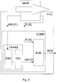
- Fig. 3 includes a memory means MEM and a filling level controller FLC.
- the memory means MEM includes a first circuit CIRC1 and a second circuit CIRC2.
- the filling level controller FLC includes a comparator COMP and two links from the memory means MEM to this comparator COMP, a first link and a second link.
- the comparator includes the transfer device TRANS of the invention and comparing means CM and the transfer device includes an encoder ENC and buffer means BUF.
- the memory means MEM is coupled to the comparator via the two links of the filling level controller FLC.
- the first link is coupled to the transfer device TRANS which is coupled to the comparing means CM and the second link is directly coupled to the comparing means CM.
- Information data (not shown in order not to overload Fig. 3) is written into the memory means MEM with a first frequency f1 whereby the first circuit CIRC1 generates the write addresses WR (f1) of this information data. These write addresses WR(f1) are successive numbers and are created with the same frequency f1 as the writing frequency f1. Later on, the information data is read from the memory means MEM with a second frequency f2 whereby the second circuit CIRC2 generates the read addresses R(f2) of this information data. These read addresses R(f2) are successive numbers and are created with the same frequency f2 as the reading frequency f2.
- the write addresses WR(f1) and read addresses R(f2) are provided via the first link and the second link, respectively, to the comparator COMP.
- the write addresses WR(f1) are compared with the read addresses R(f2). It is the intention to do this with the comparing means CM, however, both addresses are generated at a different frequency and directly comparing them would generate results with an unpredictable fault.
- transfer device TRANS is introduced in order to, following this embodiment, transfer the write addresses WR(f1) into buffered write addresses WR'(f2).
- the detailed working of the transfer device TRANS is described in the above paragraphs.
- both addresses, buffered write addresses WR'(f2) and read addresses R(f2), are provided at the same frequency f2 to the comparing means CM.
- the comparing means CM builds the difference between the buffered write addresses WR'(f2) and the read addresses R(f2) and generates thereby a results RES which is a measure for the filling level of the memory means MEM.
- the transfer device TRANS may introduce a fault of one. This fault of one may also be reflected in the result RES of the comparing means CM and has to be taken into account.
- the memory means MEM are allowed to be filled up to a predefined filling level, the result RES has to be compared with this predefined filling level minus one.
- successive numbers are neighbouring numbers which have a bigger value from one number to the other number
- the invention is not restricted to successive numbers like that, but the successive numbers may also become smaller from one number to the other number or may become now and then bigger and smaller respectively, as long as they are neighbouring numbers.
- number 0 and the maximum number to be represented in the Grey code differs from each other in only one single bit, e.g. number 0 represented in the sixteen Grey code by 0000, and number 16 represented in the sixteen Grey code by 1000 differ from each other in only the first digit. These numbers are in this embodiment also considered as being successive numbers.
- Grey reflected binary code is chosen for the successive numbers to be encoded in while being buffered
- the invention is not restricted to this Grey code, but any cyclic code whereby the representations of successive numbers differs from one to the other in only one single digit can be used for the successive numbers to be encoded in while being buffered.
- the read addresses as being successive numbers in this embodiment is no restriction on the application of the present invention, i.e. the comparator COMP.
- the only restriction given on the numbers provided to the comparator COMP is the restriction given on the numbers which are provided to the transfer device TRANS and it has to be clear that there is no restriction on the numbers provided directly to the comparing means CM.
Landscapes
- Engineering & Computer Science (AREA)
- Theoretical Computer Science (AREA)
- Physics & Mathematics (AREA)
- General Engineering & Computer Science (AREA)
- General Physics & Mathematics (AREA)
- Synchronisation In Digital Transmission Systems (AREA)
Priority Applications (1)
| Application Number | Priority Date | Filing Date | Title |
|---|---|---|---|
| EP96402588A EP0845739A1 (fr) | 1996-11-29 | 1996-11-29 | Méthode de transfert de données et son dispositif, comparateur utilisant un tel dispositif, et usage d'un tel comparateur pour contrÔler le niveau de remplissage d'une mémoire |
Applications Claiming Priority (1)
| Application Number | Priority Date | Filing Date | Title |
|---|---|---|---|
| EP96402588A EP0845739A1 (fr) | 1996-11-29 | 1996-11-29 | Méthode de transfert de données et son dispositif, comparateur utilisant un tel dispositif, et usage d'un tel comparateur pour contrÔler le niveau de remplissage d'une mémoire |
Publications (1)
| Publication Number | Publication Date |
|---|---|
| EP0845739A1 true EP0845739A1 (fr) | 1998-06-03 |
Family
ID=8225328
Family Applications (1)
| Application Number | Title | Priority Date | Filing Date |
|---|---|---|---|
| EP96402588A Withdrawn EP0845739A1 (fr) | 1996-11-29 | 1996-11-29 | Méthode de transfert de données et son dispositif, comparateur utilisant un tel dispositif, et usage d'un tel comparateur pour contrÔler le niveau de remplissage d'une mémoire |
Country Status (1)
| Country | Link |
|---|---|
| EP (1) | EP0845739A1 (fr) |
Citations (7)
| Publication number | Priority date | Publication date | Assignee | Title |
|---|---|---|---|---|
| WO1990004294A1 (fr) * | 1988-10-14 | 1990-04-19 | Digital Equipment Corporation | Procede et appareil de detection de depassement de capacite et/ou d'insuffisance imminents d'un tampon d'elasticite |
| EP0383260A2 (fr) * | 1989-02-13 | 1990-08-22 | Kabushiki Kaisha Toshiba | Circuit de tampon élastique |
| EP0391584A2 (fr) * | 1989-04-03 | 1990-10-10 | AT&T GLOBAL INFORMATION SOLUTIONS INTERNATIONAL INC. | Système de mémoire PEPS |
| US5084841A (en) * | 1989-08-14 | 1992-01-28 | Texas Instruments Incorporated | Programmable status flag generator FIFO using gray code |
| US5088061A (en) * | 1990-07-24 | 1992-02-11 | Vlsi Technology, Inc. | Routing independent circuit components |
| EP0484652A2 (fr) * | 1990-11-06 | 1992-05-13 | International Computers Limited | Tampon à premier entrée et premier sortie |
| US5426756A (en) * | 1992-08-11 | 1995-06-20 | S3, Incorporated | Memory controller and method determining empty/full status of a FIFO memory using gray code counters |
-
1996
- 1996-11-29 EP EP96402588A patent/EP0845739A1/fr not_active Withdrawn
Patent Citations (7)
| Publication number | Priority date | Publication date | Assignee | Title |
|---|---|---|---|---|
| WO1990004294A1 (fr) * | 1988-10-14 | 1990-04-19 | Digital Equipment Corporation | Procede et appareil de detection de depassement de capacite et/ou d'insuffisance imminents d'un tampon d'elasticite |
| EP0383260A2 (fr) * | 1989-02-13 | 1990-08-22 | Kabushiki Kaisha Toshiba | Circuit de tampon élastique |
| EP0391584A2 (fr) * | 1989-04-03 | 1990-10-10 | AT&T GLOBAL INFORMATION SOLUTIONS INTERNATIONAL INC. | Système de mémoire PEPS |
| US5084841A (en) * | 1989-08-14 | 1992-01-28 | Texas Instruments Incorporated | Programmable status flag generator FIFO using gray code |
| US5088061A (en) * | 1990-07-24 | 1992-02-11 | Vlsi Technology, Inc. | Routing independent circuit components |
| EP0484652A2 (fr) * | 1990-11-06 | 1992-05-13 | International Computers Limited | Tampon à premier entrée et premier sortie |
| US5426756A (en) * | 1992-08-11 | 1995-06-20 | S3, Incorporated | Memory controller and method determining empty/full status of a FIFO memory using gray code counters |
Similar Documents
| Publication | Publication Date | Title |
|---|---|---|
| US4216460A (en) | Transmission and/or recording of digital signals | |
| US4498174A (en) | Parallel cyclic redundancy checking circuit | |
| US5408498A (en) | Serial-signal transmission apparatus | |
| KR840003371A (ko) | 분할 요구 버스에 호출을 할당하기 위한 시스템 | |
| AU642547B2 (en) | First-in first-out buffer | |
| JPH0525224B2 (fr) | ||
| US6370667B1 (en) | CRC operating calculating method and CRC operational calculation circuit | |
| JPS60140982A (ja) | デジタル符号語を検出する方法および装置 | |
| US4955061A (en) | Method and apparatus for processing an image signal | |
| US6127950A (en) | Transmission circuit and reception circuit | |
| WO1999060702A1 (fr) | Compteurs faible puissance | |
| JPH0460391B2 (fr) | ||
| US3984833A (en) | Apparatus for encoding extended run-length codes | |
| US5854596A (en) | Encoding arrangement and method for encoding (n-1)-bit information words into n-bit channel words and decoding arrangement and method for decoding the channel words into information words | |
| EP0845739A1 (fr) | Méthode de transfert de données et son dispositif, comparateur utilisant un tel dispositif, et usage d'un tel comparateur pour contrÔler le niveau de remplissage d'une mémoire | |
| JPS586344B2 (ja) | フゴウカソウチ | |
| JP2689735B2 (ja) | シリアル信号切替制御回路 | |
| JPH04270569A (ja) | 画像処理装置におけるデータ圧縮方式 | |
| JPS6016772B2 (ja) | 信号伝送方式 | |
| JP2708747B2 (ja) | 画像処理装置 | |
| JPH0427754B2 (fr) | ||
| JPS60194671A (ja) | ランレングス符号化装置 | |
| JP3455828B2 (ja) | ビットシフト回路 | |
| SU1197090A2 (ru) | Устройство дл определени ранга числа | |
| JP2556160B2 (ja) | 圧縮符号伸長装置 |
Legal Events
| Date | Code | Title | Description |
|---|---|---|---|
| PUAI | Public reference made under article 153(3) epc to a published international application that has entered the european phase |
Free format text: ORIGINAL CODE: 0009012 |
|
| STAA | Information on the status of an ep patent application or granted ep patent |
Free format text: STATUS: THE APPLICATION HAS BEEN WITHDRAWN |
|
| AK | Designated contracting states |
Kind code of ref document: A1 Designated state(s): AT BE CH DE DK ES FI FR GB GR IE IT LI LU MC NL PT SE |
|
| AX | Request for extension of the european patent |
Free format text: AL;LT;LV;RO;SI |
|
| 18W | Application withdrawn |
Withdrawal date: 19980504 |