EP0845740A1 - Multipliziereinheit - Google Patents
Multipliziereinheit Download PDFInfo
- Publication number
- EP0845740A1 EP0845740A1 EP97120773A EP97120773A EP0845740A1 EP 0845740 A1 EP0845740 A1 EP 0845740A1 EP 97120773 A EP97120773 A EP 97120773A EP 97120773 A EP97120773 A EP 97120773A EP 0845740 A1 EP0845740 A1 EP 0845740A1
- Authority
- EP
- European Patent Office
- Prior art keywords
- multiplier
- unit
- multiplicand
- adder
- component
- Prior art date
- Legal status (The legal status is an assumption and is not a legal conclusion. Google has not performed a legal analysis and makes no representation as to the accuracy of the status listed.)
- Granted
Links
Images


Classifications
-
- G—PHYSICS
- G06—COMPUTING OR CALCULATING; COUNTING
- G06F—ELECTRIC DIGITAL DATA PROCESSING
- G06F7/00—Methods or arrangements for processing data by operating upon the order or content of the data handled
- G06F7/38—Methods or arrangements for performing computations using exclusively denominational number representation, e.g. using binary, ternary, decimal representation
- G06F7/48—Methods or arrangements for performing computations using exclusively denominational number representation, e.g. using binary, ternary, decimal representation using non-contact-making devices, e.g. tube, solid state device; using unspecified devices
- G06F7/52—Multiplying; Dividing
- G06F7/523—Multiplying only
- G06F7/527—Multiplying only in serial-parallel fashion, i.e. one operand being entered serially and the other in parallel
-
- G—PHYSICS
- G06—COMPUTING OR CALCULATING; COUNTING
- G06F—ELECTRIC DIGITAL DATA PROCESSING
- G06F7/00—Methods or arrangements for processing data by operating upon the order or content of the data handled
- G06F7/38—Methods or arrangements for performing computations using exclusively denominational number representation, e.g. using binary, ternary, decimal representation
- G06F7/48—Methods or arrangements for performing computations using exclusively denominational number representation, e.g. using binary, ternary, decimal representation using non-contact-making devices, e.g. tube, solid state device; using unspecified devices
- G06F7/52—Multiplying; Dividing
- G06F7/523—Multiplying only
- G06F7/53—Multiplying only in parallel-parallel fashion, i.e. both operands being entered in parallel
- G06F7/5324—Multiplying only in parallel-parallel fashion, i.e. both operands being entered in parallel partitioned, i.e. using repetitively a smaller parallel parallel multiplier or using an array of such smaller multipliers
-
- G—PHYSICS
- G06—COMPUTING OR CALCULATING; COUNTING
- G06F—ELECTRIC DIGITAL DATA PROCESSING
- G06F2207/00—Indexing scheme relating to methods or arrangements for processing data by operating upon the order or content of the data handled
- G06F2207/38—Indexing scheme relating to groups G06F7/38 - G06F7/575
- G06F2207/3804—Details
- G06F2207/386—Special constructional features
- G06F2207/388—Skewing
Definitions
- This invention relates to data processing systems and, more particularly, to data processing system multiplier components that multiply a multiplicand represented by data bits by a multiplier represented by data bits.
- multiplier units such as the booth multiplier unit or the parallel multiplier unit, typically have a low utilization of components. This low utilization is the result of the time for data to ripple through the multiplier unit.
- the ripple time results from the time for the data to be processed by the summation stage of the multiplier unit.
- carry look-ahead circuits have been implemented. However, the implementation of carry look-ahead circuits provides a significant increase in the complexity and number of components needed for the multiplier unit.
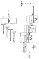
- the multiplier unit for the multiplication of a binary multiplicand A by a binary multiplier B unit can typically be divided into three stages.
- the first stage is a preprocessing of multiplic and A stored in register 10 by preprocessor stage 11 to simplify the apparatus used to implement the multiplication procedure.
- the digit generator component 13 next provides the i th digit of the multiplier B stored in register 20, i.e., B i .
- the second stage generates the product A*B i which is generated internally within the second stage or the multiplier stage 12.
- the sum of A*B i is generated, this partial product being shifted by S i , (i.e., the position of the multiplier bit B i in the multiplier register 20).
- the preprocessor stage 11 is inactive.
- the multiplier stage 12 multiplies A by either 1 or 0, this binary bit being the i th digit of B.
- the summation stage 14 shifts the products by S i and adds all the results together.
- the second or multiplier stage is relatively simple because the "digits" of the multiplier are either 1 or 0.
- the utilization of the adder components is low because in the third or summation stage 14, the additions take place serially and are added to a single running sum.
- a longer time for performing the multiplication function can be tolerated when fewer components are needed to perform the multiplication operation.
- the higher component utilization results in a greater number of processing cycles to implement a multiplication procedure.
- the multiplier stage includes a gate and shift register component which controllably transmits and shifts the multiplicand in respose to a multiplier logic signal subunit applied to the control terminal of the gate and shift component.
- the multiplier stage includes a gate component which controllably transmits an appropriately shifted multiplicand in response to a multiplier logic signal subdigit applied to the control terminal of the gate component.
- the multiplier stage also includes a plurality of adder components, each adder component being associated with a (typically multiple logic signal) digit of the multiplicand (the digit of the multiplicand being shifted in a cycle-dependent manner after the first adder unit cycle).
- First input terminals of each adder unit have delay components coupled in series, the number of delay components being a function of the position of the associated multiplicand digit and the number of digits of the multiplier.
- each adder unit is applied to a series of [N] K (K being the number of digits into which the multiplier is divided and where P is the number of digits into which the multiplicand is divided) delay components, the output of the [N] K delay components being coupled to second input terminals of the same adder component.
- [N is the number of multi-logic signal digits into which the multiplicand and the multiplier is divided.]
- the partial products A p *B k can be generated, A p and B k being multiplicand and multiplier digits, respectively.
- the partial products A*B 0 through A*B K-1 can be applied to the summation stage of the multiplier unit on successive cycles.
- the number of logic signals of the multiplier is a integer multiple of the logic signals comprising the multiplicand, the implementation of the multiplier unit is particularly convenient.
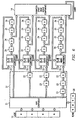
- FIG. 2 a block diagram of the second or multiplier stage 12 of a multiplier unit according to the present invention is shown.
- the multiplicand A has M logic signals and is divided into P digits or groups of logic signals, the digits being labelled A 0 -A P-1 .
- the multiplicand A is stored in register 10 shown in Fig. 1. Note that register 10 has an additional portion 29.
- the multiplicand A is shifted during the operation of the multiplier and the larger register is needed to accommodate this shifting.
- the multiplicand A is applied to a gate component 21.
- the transmission of the multiplicand A through the gate component 21 is determined by which logic bit of the multiplier B is applied to a control terminal of gate component 21.
- the gate component transmits the bits of multiplicand A or transmits the opposite logic state of the bits of multiplicand A depends of the logic state of the bit applied to the control terminal of the gate component 21.
- the multiplier B is divided into a K digits or groups of logic signals, i.e., B 0 -B K-1 .
- the transmitted signals from the gate component 21 are applied to series of P adder units 22.
- the least significant digit of multiplicand A, A 0 when transmitted by the gate component 21, is applied directly to the first (i.e., least significant) adder component 22.
- the second least significant digit of multiplicand A, A 1 when transmitted by the gate component 21, is applied through a single delay component 23 to the second (i.e., next least significant) adder component 22.
- Each additional digit of A, transmitted by the gate component 21, is applied to an associated (i.e., increasingly significant) adder component 22 through one additional delay component 23.
- the most significant digit, A P-1 when transmitted by the gate component 21, is applied to the associated adder unit 22 through K-1 delay components 23.
- the output signal of the adder units 22 are each applied to the K delay components 24 coupled in series.
- the output of the last delay component 24 is coupled to a second input terminal of the associated adder component 22.
- the least significant digit output signal is taken from the input terminal of the last of the K delay components coupled to the adder unit 22 associated with the least significant digit of the multiplicand, A 0 .
- the next least significant digit is provided from the input of the next to last delay component 24 associated with the adder component 22 receiving the next least significant digit of the multiplicand, A 1 .
- the most significant output digit is provided from the adder component 22 receiving the most significant bit from the multiplicand, A P-1 .
- a carry-out bit is applied from an adder component 22 to a carry-in terminal of the adder component 22 associated with the next higher multiplicand digit.
- the multiplier is N bits in length.
- the adder component in the multiplier stage is M+L in length and the multiplier stage adder components 22 are (M+L)/K in length] is stored in the M less significant bits of register 10 (register 10 being M+L bits in length), the M+L bits being divided into P digits with (M+L)/P logic bits.
- the adder component in the multiplier stage is M+L bits in length and each multiplier stage adder components 22 are (M+L)/P logic bits in length.
- Each adder component 22 receives its input signals one cycle or clock period after the previous adder component 22 received its input signals. Because of the reduced adder component 22 length resulting from the skewed application of partial products, the critical path is reduced.
- Fig. 3A the contents of the delay components 23 and 24 associated with the adder component 22 receiving the least significant digit from the multiplicand and the contents of delay components 23 and 24 associated with the adder unit receiving the next least significant digit from the multiplicand are shown after one time period T of operation of the multiplier unit in Fig. 2.
- Fig. 3B the contents of the same delay components 23 and 24 are shown after 5 time periods T, the multiplicand being divided into 4 digits.
- the output logic signals for partial products from the multiplier stage 12 is shown.
- M is the number of logic signals of each digit of the multiplier
- L is the number of logic signals for the multiplicand digits.
- the K partial products from the multiplier stage 12 to be applied to the summation stage 14 is L+M bits in width.
- the multiplier unit is configured wherein each of the K partial products is available on succeeding clock cycles because of the skewing resulting from the delay components 23. Each of the K partial products is shifted by L bit positions with respect to the previous partial product from the multiplier stage 12.
- FIG. 6 an implementation of the present invention for the situation wherein the multiplier B is a multiple R (i.e., 4) of the multiplicand A is shown.
- the configuration is similar to that of Fig. 2.
- the output for the least significant digit from the multiplier stage is taken from the input to the next to last delay component 24. Both of the next two digits are received from the input to the delay line 24 preceding the next to the last delay line 24.
- the most significant digit is taken from the output of the adder unit 22, i.e., the adder unit 22 associated with the most significant digit of the multiplicand.
- the most significant half of the output signals of the multiplier stage 12 are delayed by one cycle or time period compared to the least significant half of the signals.
- the present invention can be understood in the following manner.
- the partial product of B 00 i.e., the first bit of the first multiplier digit
- multiplicand A is entered in the adder units (and adder unit is includes the adder and delay components) and stored.
- the partial product of B 10 (the first bit of the second multiplier digit) is then entered in the adder unit and stored. This process is continued until all the partial products of the multiplicand A and all the first bits of the multiplier digits are stored ⁇ i.e., A*(B 00 +...+B (K-1)0 ) ⁇ .
- multiplicand A is shifted in register 10 one bit position and the foregoing process is repeated with the exception that the partial products of the same multiplier digit position are combined. This process is repeated for each bit position of the multiplier digits.
- the delay components 24 accumulate partial products of A p *B k .
- the K partial products from the multiplier stage 12 are shifted by Ki increments and the K partial products cn be processed separately or combined.
- Fig. 5 also illustrates a carry ripple of length L-M. Provided L>M, addition in the summation stage can be performed using a length M adder and a length L-M carry propagate unit. Thus the summation stage can be implemented by a fast shift of length L and an M bit adder unit.
- the adder of the present invention can be implemented as shown in Fig. 5.
- the most significant half of the multiplier stage at time period T is added to the least significant half at time T+1.
- the resultant carry is then carried into the next add operation.
- the partial products leave the multiplier in M slices.
- the most significant and least significant portions can be directly added to produce the desired result (except that the first output is the least significant half).
- the gate and shift component which is included in the general implementation can be included in the shift operation of the preprocessor stage 11.
- the present invention results in a greater usage of components at the expense of additional latency.
- the adder units 22 are used a multiplicity of times during the accumulation of the A p *B k partial products.
- the summation stage includes a ripple carry of length L-M bits that connects the carry-out of addition to the carry-in of the another addition.
- L>M the addition is simplified because the addition can be performed with an adder of length M bit positions and a length L-M bit position carry propagate unit.
- L-M 0, only a routing of length L and an M bit adder unit with carry apparatus is needed to implement the summation stage.
- the present invention is intended to utilize less apparatus while requiring a greater number of cycles to execute the multiplication operation.
- the latency for the partial product A 0 *B 0 is N cycles, while the latency for the partial product A*B 0 is N+K-1 cycles.
- the latency can be reduced by increasing the amount of apparatus. For example, by appropriate increase in the complexity of the apparatus of the gate component 21, two (or more) bits from the multiplier B could be applied added to the gate component 21 and these bits "encoded" with multiplicand A before being applied to the remainder of the multiplier stage. The latency can thus be improved, but at the expense of an increase in the amount of apparatus.
- the delay components coupled to the input terminals of the adder components can be eliminated by increasing the complexity of the gate component, i.e., by appropriate shifting (or routing) of portions of the multiplicand A.
Landscapes
- Physics & Mathematics (AREA)
- General Physics & Mathematics (AREA)
- Engineering & Computer Science (AREA)
- Computational Mathematics (AREA)
- Mathematical Analysis (AREA)
- Mathematical Optimization (AREA)
- Pure & Applied Mathematics (AREA)
- Theoretical Computer Science (AREA)
- Computing Systems (AREA)
- General Engineering & Computer Science (AREA)
- Complex Calculations (AREA)
Applications Claiming Priority (2)
| Application Number | Priority Date | Filing Date | Title |
|---|---|---|---|
| US3250296P | 1996-11-27 | 1996-11-27 | |
| US32502P | 1996-11-27 |
Publications (2)
| Publication Number | Publication Date |
|---|---|
| EP0845740A1 true EP0845740A1 (de) | 1998-06-03 |
| EP0845740B1 EP0845740B1 (de) | 2002-09-18 |
Family
ID=21865268
Family Applications (1)
| Application Number | Title | Priority Date | Filing Date |
|---|---|---|---|
| EP19970120773 Expired - Lifetime EP0845740B1 (de) | 1996-11-27 | 1997-11-26 | Multipliziereinheit |
Country Status (4)
| Country | Link |
|---|---|
| EP (1) | EP0845740B1 (de) |
| JP (1) | JP3848764B2 (de) |
| DE (1) | DE69715570T2 (de) |
| TW (1) | TW381232B (de) |
Citations (2)
| Publication number | Priority date | Publication date | Assignee | Title |
|---|---|---|---|---|
| US4811269A (en) * | 1985-10-09 | 1989-03-07 | Hitachi, Ltd. | Bit slice multiplication circuit |
| EP0517241A2 (de) * | 1991-06-06 | 1992-12-09 | Lsi Logic Corporation | Verschachtelter Multiplizier-Akkumulator |
-
1997
- 1997-11-26 DE DE1997615570 patent/DE69715570T2/de not_active Expired - Lifetime
- 1997-11-26 EP EP19970120773 patent/EP0845740B1/de not_active Expired - Lifetime
- 1997-11-27 TW TW86117817A patent/TW381232B/zh not_active IP Right Cessation
- 1997-11-27 JP JP32654997A patent/JP3848764B2/ja not_active Expired - Fee Related
Patent Citations (2)
| Publication number | Priority date | Publication date | Assignee | Title |
|---|---|---|---|---|
| US4811269A (en) * | 1985-10-09 | 1989-03-07 | Hitachi, Ltd. | Bit slice multiplication circuit |
| EP0517241A2 (de) * | 1991-06-06 | 1992-12-09 | Lsi Logic Corporation | Verschachtelter Multiplizier-Akkumulator |
Non-Patent Citations (3)
| Title |
|---|
| D. ESTEBAN: "TIME-SHARED SHIFT ACCUMULATOR", IBM TECHNICAL DISCLOSURE BULLETIN., vol. 15, no. 3, August 1972 (1972-08-01), NEW YORK US, pages 763 - 764, XP002056987 * |
| P. BUCKLE ET AL.: "Programmable shift registers for numerical multiplication", RADIO AND ELECTRONIC ENGINEER., vol. 44, no. 1, January 1974 (1974-01-01), LONDON GB, pages 33 - 38, XP002056988 * |
| XINGCHA FAN ET AL: "DATA FORMATS AND ARITHMETIC OPERATORS FOR SERIAL/PARALLEL TRADE- OFFS IN PIPELINED ARCHITECTURES", PROCEEDINGS OF THE INTERNATIONAL SYMPOSIUM ON CIRCUITS AND SYSTEMS, NEW ORLEANS, MAY 1 - 3, 1990, vol. 2 OF 4, 1 May 1990 (1990-05-01), INSTITUTE OF ELECTRICAL AND ELECTRONICS ENGINEERS, pages 1248 - 1251, XP000167038 * |
Also Published As
| Publication number | Publication date |
|---|---|
| TW381232B (en) | 2000-02-01 |
| JPH10161853A (ja) | 1998-06-19 |
| JP3848764B2 (ja) | 2006-11-22 |
| DE69715570T2 (de) | 2003-08-07 |
| EP0845740B1 (de) | 2002-09-18 |
| DE69715570D1 (de) | 2002-10-24 |
Similar Documents
| Publication | Publication Date | Title |
|---|---|---|
| US4994997A (en) | Pipeline-type serial multiplier circuit | |
| US6601077B1 (en) | DSP unit for multi-level global accumulation | |
| US4156922A (en) | Digital system for computation of the values of composite arithmetic expressions | |
| US4965762A (en) | Mixed size radix recoded multiplier | |
| US4796219A (en) | Serial two's complement multiplier | |
| US5396445A (en) | Binary carry-select adder | |
| US4142242A (en) | Multiplier accumulator | |
| US6735167B1 (en) | Orthogonal transform processor | |
| US5212782A (en) | Automated method of inserting pipeline stages in a data path element to achieve a specified operating frequency | |
| US7039091B1 (en) | Method and apparatus for implementing a two dimensional correlator | |
| JPS5981761A (ja) | シストリツク計算配列 | |
| EP0845740A1 (de) | Multipliziereinheit | |
| US5889691A (en) | Apparatus and method for a multiplier unit with high component utilization | |
| EP0478264B1 (de) | Digitaler Wobleroszillator | |
| EP0499412B1 (de) | Multiplizierer-Schaltungen mit seriellem Eingang | |
| US5948051A (en) | Device improving the processing speed of a modular arithmetic coprocessor | |
| US5258945A (en) | Method and apparatus for generating multiples of BCD number | |
| US4849758A (en) | System for transmitting or storing input signals | |
| US6651079B1 (en) | High speed pipeline multiplier with virtual shift | |
| RU2837596C1 (ru) | Многоканальный накапливающий сумматор по произвольным модулям | |
| US6067331A (en) | System and method for binary correlation | |
| SU1667059A2 (ru) | Устройство дл умножени двух чисел | |
| US6004022A (en) | Product sum operation apparatus | |
| RU2799035C1 (ru) | Конвейерный сумматор по модулю | |
| RU2021633C1 (ru) | Устройство для умножения чисел |
Legal Events
| Date | Code | Title | Description |
|---|---|---|---|
| PUAI | Public reference made under article 153(3) epc to a published international application that has entered the european phase |
Free format text: ORIGINAL CODE: 0009012 |
|
| AK | Designated contracting states |
Kind code of ref document: A1 Designated state(s): DE FR GB IT NL |
|
| AX | Request for extension of the european patent |
Free format text: AL;LT;LV;MK;RO;SI |
|
| 17P | Request for examination filed |
Effective date: 19981203 |
|
| AKX | Designation fees paid |
Free format text: DE FR GB IT NL |
|
| RBV | Designated contracting states (corrected) |
Designated state(s): DE FR GB IT NL |
|
| 17Q | First examination report despatched |
Effective date: 20010206 |
|
| GRAG | Despatch of communication of intention to grant |
Free format text: ORIGINAL CODE: EPIDOS AGRA |
|
| GRAG | Despatch of communication of intention to grant |
Free format text: ORIGINAL CODE: EPIDOS AGRA |
|
| GRAG | Despatch of communication of intention to grant |
Free format text: ORIGINAL CODE: EPIDOS AGRA |
|
| GRAH | Despatch of communication of intention to grant a patent |
Free format text: ORIGINAL CODE: EPIDOS IGRA |
|
| GRAH | Despatch of communication of intention to grant a patent |
Free format text: ORIGINAL CODE: EPIDOS IGRA |
|
| GRAA | (expected) grant |
Free format text: ORIGINAL CODE: 0009210 |
|
| AK | Designated contracting states |
Kind code of ref document: B1 Designated state(s): DE FR GB IT NL |
|
| PG25 | Lapsed in a contracting state [announced via postgrant information from national office to epo] |
Ref country code: NL Free format text: LAPSE BECAUSE OF FAILURE TO SUBMIT A TRANSLATION OF THE DESCRIPTION OR TO PAY THE FEE WITHIN THE PRESCRIBED TIME-LIMIT Effective date: 20020918 Ref country code: IT Free format text: LAPSE BECAUSE OF FAILURE TO SUBMIT A TRANSLATION OF THE DESCRIPTION OR TO PAY THE FEE WITHIN THE PRESCRIBED TIME-LIMIT;WARNING: LAPSES OF ITALIAN PATENTS WITH EFFECTIVE DATE BEFORE 2007 MAY HAVE OCCURRED AT ANY TIME BEFORE 2007. THE CORRECT EFFECTIVE DATE MAY BE DIFFERENT FROM THE ONE RECORDED. Effective date: 20020918 |
|
| REG | Reference to a national code |
Ref country code: GB Ref legal event code: FG4D |
|
| REF | Corresponds to: |
Ref document number: 69715570 Country of ref document: DE Date of ref document: 20021024 |
|
| NLV1 | Nl: lapsed or annulled due to failure to fulfill the requirements of art. 29p and 29m of the patents act | ||
| ET | Fr: translation filed | ||
| PLBE | No opposition filed within time limit |
Free format text: ORIGINAL CODE: 0009261 |
|
| STAA | Information on the status of an ep patent application or granted ep patent |
Free format text: STATUS: NO OPPOSITION FILED WITHIN TIME LIMIT |
|
| 26N | No opposition filed |
Effective date: 20030619 |
|
| PGFP | Annual fee paid to national office [announced via postgrant information from national office to epo] |
Ref country code: DE Payment date: 20121130 Year of fee payment: 16 Ref country code: FR Payment date: 20121113 Year of fee payment: 16 |
|
| PGFP | Annual fee paid to national office [announced via postgrant information from national office to epo] |
Ref country code: GB Payment date: 20121025 Year of fee payment: 16 |
|
| GBPC | Gb: european patent ceased through non-payment of renewal fee |
Effective date: 20131126 |
|
| REG | Reference to a national code |
Ref country code: FR Ref legal event code: ST Effective date: 20140731 |
|
| PG25 | Lapsed in a contracting state [announced via postgrant information from national office to epo] |
Ref country code: DE Free format text: LAPSE BECAUSE OF NON-PAYMENT OF DUE FEES Effective date: 20140603 |
|
| REG | Reference to a national code |
Ref country code: DE Ref legal event code: R119 Ref document number: 69715570 Country of ref document: DE Effective date: 20140603 |
|
| PG25 | Lapsed in a contracting state [announced via postgrant information from national office to epo] |
Ref country code: GB Free format text: LAPSE BECAUSE OF NON-PAYMENT OF DUE FEES Effective date: 20131126 Ref country code: FR Free format text: LAPSE BECAUSE OF NON-PAYMENT OF DUE FEES Effective date: 20131202 |