EP0845746A2 - Dispositif CAO pour cartes à circuit imprimé qui détermine les valeurs de paramètre de conception - Google Patents
Dispositif CAO pour cartes à circuit imprimé qui détermine les valeurs de paramètre de conception Download PDFInfo
- Publication number
- EP0845746A2 EP0845746A2 EP97309576A EP97309576A EP0845746A2 EP 0845746 A2 EP0845746 A2 EP 0845746A2 EP 97309576 A EP97309576 A EP 97309576A EP 97309576 A EP97309576 A EP 97309576A EP 0845746 A2 EP0845746 A2 EP 0845746A2
- Authority
- EP
- European Patent Office
- Prior art keywords
- design
- parameter
- design parameter
- parameter determination
- values
- Prior art date
- Legal status (The legal status is an assumption and is not a legal conclusion. Google has not performed a legal analysis and makes no representation as to the accuracy of the status listed.)
- Withdrawn
Links
Images


Classifications
-
- G—PHYSICS
- G06—COMPUTING OR CALCULATING; COUNTING
- G06F—ELECTRIC DIGITAL DATA PROCESSING
- G06F30/00—Computer-aided design [CAD]
- G06F30/30—Circuit design
- G06F30/39—Circuit design at the physical level
Definitions
- the present invention relates to a CAD (Computer Aided Design) apparatus for designing a printed circuit board, the printed circuit board CAD apparatus especially for supporting a determination of unknown design parameter values.
- CAD Computer Aided Design
- Printed circuit board CAD apparatuses have been widely used for designing printed circuit boards.
- Fig. 1 is a block diagram showing a widely-used printed circuit board CAD apparatus.
- conventional printed circuit board CAD apparatus 700 includes: input reception unit 701 for receiving user input from input apparatus 710 and external storage apparatus 720; design information storage unit 702 for storing design parameter values inputted from the input reception unit 701, such as circuit information, component information, and board information; and layout unit 703 for interactively or automatically laying out components and wires on a printed circuit board in accordance with the circuit information and other information stored in the design information storage unit 702 and instructions inputted from the input reception unit 701.
- Display apparatus 730 displays and print apparatus 740 prints out the layout result outputted from the layout unit 703.
- a user first inputs design parameter values composed of circuit information, component information, and board information which are necessary for designing a printed circuit board, via the input apparatus 710.
- the circuit information is information on wires between components
- the component information is on types and sizes of components to be used
- the board information is on a size of the printed circuit board and a number of layers of the printed circuit board.
- the inputted information is stored in the design information storage unit 702 via the input reception unit 701.
- the layout unit 703 then automatically or interactively generates a virtual layout of components and wires on the printed circuit board in accordance with conditions set by the design parameter values stored in the design information storage unit 702.
- design parameter values such as foil width and terminating resistance value based on their years of experience and results of analysis, and wire the lines in accordance with the determined design parameter values.
- Causes of malfunctions due to electromagnetic noise include crosstalk, which is to say, changes of signal values of one signal line caused by electromagnetic induction and coupling of an adjacent signal line.
- a wiring technique has been developed so that a crosstalk coefficient which is one of the design parameters is set below a reference value. This technique specifically relates to automatic wiring where factors which determine the value of the crosstalk coefficient, such as length of parallel lines and distance between the lines are controlled.
- the conventional printed circuit board CAD apparatuses described above need expert designers who are capable of determining appropriate design parameter values which have to be calculated before operating the CAD apparatuses. This causes difficulties in designing appropriate printed circuit boards.
- a design parameter value is often determined by a plurality of factors, some of which cannot be found only from information such as design specifications.
- the designers have to appropriately determine such factors based on experience. If the designers are inexperienced, it may be very difficult to appropriately determine these factors.
- a critical network such as a clock is wired manually in accordance with design conditions specified by professionals and expert designers.
- skill and experience are essential for designing circuit boards while optimizing design parameter values through the use of the printed circuit board CAD apparatuses.
- the above-mentioned printed circuit board CAD apparatuses which design printed circuit boards by adjusting the design parameter values have a problem in that they are incapable of adjusting design parameter values other than those which are adjustable during the generation of the layout.
- a printed circuit board CAD apparatus for controlling the wiring to set the crosstalk coefficient below the reference value described above is designed to control only the design parameter values adjustable during the generation of the layout, such as the length of the parallel lines and the distance between the lines.
- Factors which determine the crosstalk coefficient include not only factors which can be adjusted during the generation of the layout, such as the length of the parallel lines and the distance between the lines, but also factors which cannot be adjusted during the generation of the layout, such as distance between layers, foil width, and circuit board material.
- the above object can be fulfilled by determining unknown design parameter values from known design parameter values through the use of a plurality of rules concerning the design parameters and a plurality of formulas including the design parameters.
- unknown design parameter values are all design parameter values other than the known design parameter values, which are to be determined through the use of the rules and the formulas.
- an unknown design parameter is set to a desired value using the rules and the formulas with the known design parameter values, the set design parameter value then being used to determine other unknown design parameter values using other rules and formulas.
- design parameter values which are difficult to be predetermined can be determined appropriately.
- design parameter values are adjusted not during the generation of the layout but when the unknown design parameter values are determined, a determination of optimal design parameter values is possible by controlling all factors that determine the design parameter values, so that design flexibility can be improved.
- the unknown design parameter values to be determined through the use of the rules and the formulas can be set as design parameter values relating to at least one of a wire and a board. Since there is a good possibility that the designers have to set such unknown design parameters to be determined at arbitrary values, printed circuit board design can be highly efficient by using the printed circuit board CAD apparatus of the present invention.
- the design parameter values can be redetermined through the use of the rules and the formulas by fixing the design parameter value in violation.
- the design parameter value which violates any of the rules and the formulas can be made into an appropriate design parameter value which satisfies the rules and the formulas by adjusting design parameter values other than the design parameter value which violates any of the rules and the formulas. Then, by regenerating the layout through the use of the newly acquired design parameter values, a layout of the printed circuit board which does not violate the rules and formulas for the determined design parameter values can be created. By doing so, effective tradeoffs are made between the design parameter values, and a more appropriate printed circuit board can be designed. Also, since it is possible to fix the design parameter value which violates any of the rules and the formulas after the generation of the layout and to change other design parameter values without restriction, the printed circuit board can be designed with greater flexibility in the present invention than in the conventional method.
- an execution order of the rules and the formulas can be determined based on a specified standard. By doing so, the execution order can be determined so that design parameters included in at least two out of a plurality of rules and a plurality of formulas can be appropriately traded off in order to avoid producing design parameter values that violate the rules and the formulas, and the printed circuit board can be designed using more appropriately determined design parameter values.
- Fig. 2 is a diagram showing the hardware construction of the printed circuit board CAD apparatus of the present embodiment.
- this printed circuit board CAD apparatus includes: CPU 101 for conducting arithmetic processing; ROM 102 for storing a program and other information; RAM 103 as a work area for the CPU 101; external storage apparatus 104 such as a hard disc for storing various sets of design data and other data; input apparatus 105 such as a mouse and a keyboard for receiving user input; print apparatus 106 such as a printer; and display apparatus 107 such as a CRT.
- the present printed circuit board CAD apparatus achieves the functions explained below using the program stored in the ROM 102. It should be noted here that this printed circuit board CAD apparatus can also be realized by installing an executable program which has the functions and the operations explained below into a general-purpose computer. Such a program can be recorded on a computer-readable recording medium such as a floppy disk.
- Fig. 3 is a function block diagram showing the present printed circuit board CAD apparatus 200.
- the printed circuit board CAD apparatus 200 functionally comprises: input reception unit 201; design information storage unit 202; layout unit 203; first parameter determination units 204a, 204b, ... ; second parameter determination units 205a, 205b, 205c, ... ; parameter determination order decision unit 206; and parameter determination re-execution instruction unit 207.
- the input reception unit 201 is connected to the input apparatus 105 and the external storage apparatus 104, while the layout unit 203 is connected to the display apparatus 107 and the print apparatus 106.
- the input reception unit 201 receives user input of known design parameter values among design parameters including circuit information, component information, and board information via the external storage apparatus 104 and the input apparatus 105.
- the input reception unit 201 also receives instructions from the user.
- the design information storage unit 202 comprises circuit information storage unit 202a for storing circuit information, component information storage unit 202b for storing component information, and board information storage unit 202c for storing board information.
- the design information storage unit 202 stores the known design parameter values received by the input reception unit 201 and design parameter values determined by the first and second parameter determination units 204a, 204b, ... , 205a, 205b, 205c ....
- the first parameter determination units 204a, 204b, ... determine unknown design parameter values from known design parameter values using rules concerning the design parameters.
- the known design parameter values include the design parameter values received by the input reception unit 201 and the design parameter values already determined by the first and second parameter determination units 204a, 204b, ..., 205a, 205b, 205c, .... These known design parameter values are stored in the design information storage unit 202.
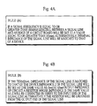
- Fig. 4A and Fig. 4B Examples of the rules concerning the design parameters are shown in Fig. 4A and Fig. 4B.
- Fig. 4A and Fig. 4B respectively show rule (A) and rule (B) of the first parameter determination units 204a and 204b.
- each "rule” is composed of a “condition” and a "result,” so that design parameter values are determined in accordance with conditions.
- the "rule” defines functional conditions to be satisfied by the design parameters, and includes rules which are determined based on product specifications such as size of a circuit board, as well as rules which are determined based on physical conditions such as electromagnetic characteristics.
- rule (A) of the first parameter determination unit 204a specifies that if a signal frequency is equal to or greater than 10[MHz], either length L between a signal line and an edge of a circuit board will be set to a value equal to or greater than 10[mm], or terminal impedance of the signal line will be matched to that of a device to which the signal line is connected. Accordingly, in the case of the signal line X in Fig.
- the signal frequency is 20[MHz], which is greater than 10[MHz]
- either the length L between the signal line X and the edge of the circuit board is set to, for instance, 15[mm] which is greater than 10[mm] or the terminal impedance of the signal line is matched to that of the device D.
- the signal frequency is below 10[MHz]
- the length L between the signal line X and the edge of the circuit board is not set at a particular value nor is the terminal impedance of the signal line matched to that of the device D.
- Rule (A) is explained as follows.
- the signal line is a high-speed signal line with a fundamental frequency greater than 10[MHz]
- a micro strip is used for wiring transmission lines symmetrical with respect to the wiring direction in order to suppress unbalanced currents which cause radiant noise and in order to reduce electromagnetic radiant noise.
- So rule (A) specifies that such a signal line should be wired at least 10[mm] inside the edge of the circuit board in order to control the distance between the line and the edge of the circuit board.
- rule (A) also specifies the matching of the terminal impedance of the signal line to that of the device as another option when the fundamental signal frequency exceeds 10[MHz].
- Rule (B) of the first parameter determination unit 204b specifies that, if the terminal impedance of the signal line is to be matched to that of the device, either the impedance Z of the signal line will be set at the output impedance "Z out"[ ⁇ ] or a resistor whose impedance is the same as the impedance Z of the signal line will be connected in series to the input end of the signal line or will be grounded from the output end of the signal line.
- rule (B) specifies these options as methods for matching the terminal impedance of the signal line to that of the device.
- the impedance Z of the signal line X is set at "Z out”.
- rule (A) of the first parameter determination unit 204a and rule (B) of the first parameter determination unit 204b are specified for a signal line. By applying these rules to each signal line on a printed circuit board, design parameter values such as impedance of each signal line are determined.
- the known design parameter values already stored in the design information storage unit 202 are not redetermined.
- the first parameter determination units 204a, 204b, ... only judge whether these design parameter values satisfy the rules of the first parameter determination units 204a, 204b ....
- the first parameter determination units 204a, 204b, ... output an error message which is then displayed on the display apparatus 107.
- the second parameter determination units 205a, 205b, 205c, ... judge whether design parameter values satisfy formulas including the design parameters.
- the second parameter determination units 205a, 205b, 205c, ... use the formulas and the known design parameter values in order to determine unknown design parameter values.
- the known design parameter values used here have been stored in the design information storage unit 202 as described above.
- Figs. 6A, 6B, and 6C show specific examples of the formulas which include design parameters and which are based on design information.
- Figs. 6A, 6B, and 6C respectively show formula (A), set of formulas (B), and set of formulas (C) of the second parameter determination units 205a, 205b, and 205c.
- These formulas are relational formulas which should be satisfied by the design parameter values, and include not only formulas concerning interrelations between a plurality of design parameters but also formulas concerning only one design parameter. While in principle known formulas are used by the second parameter determination units, new formulas can also be specified and used.
- Formula (A) of the second parameter determination unit 205a sets distance h1 between the power layer and the ground layer shown in Fig. 5B to 200[ ⁇ m] or smaller in order to shorten the distance h1 and reduce the impedance of the power supply.
- the distance h1 between the power layer and the ground layer shown in Fig. 5B is set to 100[ ⁇ m].
- Set of formulas (B) of the second parameter determination unit 205b relates to interrelations among impedance Z of a wired line, foil width w, foil thickness t, board thickness h, distance h1 between power layer and ground layer, and distance h2 between power layer and signal layer shown in Fig. 5A and Fig. 5B.
- the second parameter determination unit 205b uses known design parameter values stored in the design information storage unit 202, such as the impedance Z and the distance hl between the power layer and the ground layer if these have been already stored in the design information storage unit 202, to determine unknown design parameter values such as the foil width w, the foil thickness t, the board thickness h, and the distance h2 between the power layer and the signal layer.
- Set of formulas (C) of the second parameter determination unit 205c is composed of a formula which sets crosstalk coefficient Kb to a value equal to or smaller than inputted value "Kb max" in order to prevent crosstalk and a formula which shows interrelations among the crosstalk coefficient Kb, the foil width w, the foil thickness t, distance s between parallel lines, length 1 of the parallel lines, and the distance h2 between the power layer and the signal layer.
- the second parameter determination unit 205c sets values of the foil width w, the foil thickness t, the distance s between the parallel lines, the length 1 of the parallel lines, and the distance h2 between the power layer and the signal layer so that the crosstalk coefficient Kb can be equal to or smaller than "Kb max", at the same time setting a value of the crosstalk coefficient Kb.
- Set of formulas (B) of the second parameter determination unit 205b and set of formulas (C) of the second parameter determination unit 205c are also specified for each signal line, like the above-described rules of the first parameter determination units.
- these formulas are used to calculate unknown design parameter values through the use of known design parameter values stored in the design information storage unit 202. It should be noted here that there is a possibility that an unknown design parameter cannot be set to a particular value due to lack of a number of known design parameter values necessary for determining the unknown design parameter value. When this happens, a process is performed where several unknown design parameters are given arbitrary values so that all unknown design parameters in the formulas are determined so as to satisfy the formulas.
- the design parameters also include various parameters such as height of dielectric [ ⁇ m], height of a component [mm], power consumption [mW], rise time [nsec], fall time [nsec], and input capacitance [pF], which can be defined in accordance with various circumstances.
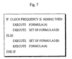
- the parameter determination order decision unit 206 decides an execution order of the first parameter determination units 204a, 204b, ... and the second parameter determination units 205a, 205b, 205c, ... based on a specified standard. Since some of the design parameters are included in at least two out of a plurality of the rules of the first parameter determination units 204a, 204b, ... and a plurality of the formulas of the second parameter determination units 205a, 205b, 205c, ... as shown in Figs. 4A, 4B, 6A, 6B, and 6C, "conflict" occurs during a determination of the design parameter values.
- the parameter determination order decision unit 206 decides the execution order of the first parameter determination units 204a, 204b, ... and the second parameter determination units 205a, 205b, 205c, ....
- the parameter determination order decision unit 206 sets an instruction shown in Fig. 7 so that, if the clock frequency is equal to or lower than 10[MHz], formula (A) is the first to be executed by the second parameter determination unit 205a to set a value of the distance hl between the power layer and the ground layer before set of formulas (B) is executed by the second parameter determination unit 205b to set values of the impedance Z and other design parameters.
- the parameter determination order decision unit 206 also decides that if the clock frequency is greater than 10[MHz], the above execution order is to be performed in reverse, that is, set of formulas (B) is the first to be executed by the second parameter determination unit 205b to simultaneously set values of the impedance Z and the distance hl between the power layer and the ground layer, before executing formula (A) by the second parameter determination unit 205a.
- set of formulas (B) is the first to be executed by the second parameter determination unit 205b to simultaneously set values of the impedance Z and the distance hl between the power layer and the ground layer, before executing formula (A) by the second parameter determination unit 205a.
- the second parameter determination unit 205a since the distance hl between the power layer and the ground layer has already been determined as described above, the second parameter determination unit 205a only judges whether the determined value of the distance hl between the power layer and the ground layer satisfies formula (A). When the determined value of the distance hl between the power layer and the ground
- the reason for changing the execution order in the above case is that the shorter the distance hl between the power layer and the ground layer, the more stable the power supply will be, while the value of the impedance should be given priority if the clock frequency is greater than 10[MHz].
- the distance hl between the power layer and the ground layer is given priority in the determination order in order to stabilize the power supply, while in the case of a high-speed signal with clock frequency exceeding 10[MHz], the impedance Z is given priority in the determination order in order to determine the value of the impedance Z first.
- the execution order may be determined so that among the rules and the formulas of the first and second parameter determination units 204a, 204b, ... 205a, 205b, 205c, ... , a parameter determination unit which determines a small number of design parameter values is given priority in the execution order.
- a parameter determination unit which determines a small number of design parameter values is given priority in the execution order.
- the parameter determination order decision unit 206 need not decide the execution order of all of the first and second parameter determination units at a same time, and may instead decide a next parameter determination unit in the execution order after each execution by one of the first and the second parameter determination units.
- the layout unit 203 automatically or interactively lays out components and wires on a printed circuit board in accordance with the design parameter values stored in the design information storage unit 202.
- the layout processing is continued, ignoring the violation.
- the parameter determination re-execution instruction unit 207 fixes the design parameter value in violation and instructs first and second parameter determination units relating to the design parameter in violation to re-execute the determination of the design parameter values.
- the parameter determination re-execution instruction unit 207 instructs the first parameter determination units 204a, 204b, ... and the second parameter determination units 205a, 205b, 205c, ... to execute and to extract design parameter values in violation of any of the rules and the formulas out of all of the design parameter values acquired after the generation of the layout.
- the parameter determination re-execution instruction unit 207 fixes the design parameter value in violation, resets design parameter values other than the design parameter value in violation, and instructs the first and second parameter determination units which have any of the rules and the formulas relating to the design parameter in violation to re-execute the determination of the design parameter values.
- the parameter determination re-execution instruction unit 207 further instructs first and second parameter determination units relating to the affected design parameter values to re-execute the determination of the design parameter values.
- the parameter determination re-execution instruction unit 207 fixes the length 1 of the parallel lines after the generation of the layout and instructs parameter determination units which relate to the crosstalk coefficient Kb or the length 1 of the parallel lines among the first and second parameter determination units 204a, 204b, ... , 205a, 205b, 205c, ... to re-execute the determination of the design parameter values.
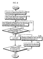
- Fig. 8 is a flowchart showing the operation of the printed circuit board CAD apparatus.
- a user inputs known design parameter values including circuit information, component information, and board information which have been predetermined based on information such as design specifications via the input apparatus 105 or the external storage apparatus 104 (S101). These inputted known design parameter values are received by the input reception unit 201 of the printed circuit board CAD apparatus, and stored in the design information storage unit 202.
- the parameter determination order decision unit 206 decides an execution order of the first parameter determination units 204a, 204b, ... and the second parameter determination units 205a, 205b, 205c, ... based on the known design parameter values stored in the design information storage unit 202 (S102).
- the first parameter determination units 204a, 204b, ... and the second parameter determination units 205a, 205b, 205c, ... determine unknown design parameter values in accordance with the execution order decided by the parameter determination order decision unit 206 (S103).
- These design parameter values determined by the first parameter determination units 204a, 204b, ... and the second parameter determination units 205a, 205b, 205c, ... are then stored in the design information storage unit 202.
- each appropriate design parameter value is stored one after another in the design information storage unit 202.
- An example of such a process is that, after setting impedance Z of a wired line at an appropriate value through the use of rule (B) of the first parameter determination unit 204b, other design parameter values are determined by set of formulas (B) of the second parameter determination unit 205b using the set value of the impedance z.
- the layout unit 203 automatically or interactively lays out a printed circuit board based on the design parameter values stored in the design information storage unit 202 (S105).
- each of the design parameter values is judged to see whether it violates any rule or formula for the design parameter value stored in the design information storage unit 202 (S106).
- the operation of the printed circuit board CAD apparatus is completed.
- the parameter determination re-execution instruction unit 207 fixes the design parameter value in violation (S107), and instructs parameter determination units relating to the design parameter in violation among the first and second parameter determination units 204a, 204b, ... , 205a, 205b, 205c, ...
- the layout unit 203 regenerates the layout of the printed circuit board using the newly determined design parameter values. This process is repeated until all of the design parameter values acquired after the generation of the layout do not violate the rules and formulas for the resign parameter values stored in the design information storage unit 202. When the layout is generated with no design parameter values in violation of the rules and the formulas, the operation of the printed circuit board design is completed.
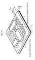
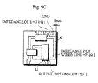
- a process of determining design parameter values and a layout of signal line X in designing a printed circuit board shown in Fig. 9A is explained.
- the determination process is shown in Fig. 9B.
- the signal line X is set such that impedance of the wired line is "Z”, signal direction is "i”, and the output impedance of the device D from which the signal is outputted is "Z out”.
- the length L between the signal line X and the edge of the circuit board is set at 15[mm] which is longer than 10[mm] based on rule (A) in Fig. 4A, while the terminal impedance of the signal line is not matched to that of the device D.
- Rule (B) in Fig. 4B is thus not enforced, as the rule (B) does not apply to this case.
- the impedance z of the signal line X is set to 75[ ⁇ ] (Fig. 9B 2 ⁇ ).
- the printed circuit board is laid out using the known design parameter values. It is supposed here that the length L between the signal line X and the edge of the circuit board becomes 5[mm] as a result of the generation of the layout. This value of the length L between the signal line X and the edge of the circuit board violates rule (A) in Fig. 4A. Accordingly, the parameter determination re-execution instruction unit 207 fixes the value of the length L between the signal line X and the edge of the circuit board at 5[mm], and instructs the first parameter determination units 204a, 204b, ... and the second parameter determination units 205a, 205b, 205c, ... to re-execute the determination of the design parameter values.
- rule (A) in Fig. 4A is enforced again, and this time it is determined that the terminal impedance of the signal line X will be matched to that of the device D, since the length L between the signal line and the edge of the circuit board has been fixed at 5[mm]. Accordingly, rule (B) in Fig. 4B applies to this case, so that the procedure of matching the terminal impedance of the signal line X to that of the device D is chosen. Since the value of "Z out" is not equal to Z in this example, it is decided to ground a resistor R with impedance of 75[ ⁇ ] from the output end of the signal line X (Fig. 9B 4 ⁇ ). By the above procedure, the violation concerning the signal line X is overcome, and the design parameter values and the layout of the signal line X are determined as shown in Fig. 9C.
- design parameter values in violation of rules or formulas exist, it is also possible for the user to edit design parameters, such as by changing of the design parameter values in violation of the rules or the formulas and the related design parameter values before the re-execution of the design parameter determination, while in the present embodiment all design parameter values in violation are fixed, and the first and second parameter determination units which have the rules and the formulas concerning the design parameters in violation re-execute the determination of the design parameter values.
Landscapes
- Engineering & Computer Science (AREA)
- Computer Hardware Design (AREA)
- Physics & Mathematics (AREA)
- Theoretical Computer Science (AREA)
- Evolutionary Computation (AREA)
- Geometry (AREA)
- General Engineering & Computer Science (AREA)
- General Physics & Mathematics (AREA)
- Design And Manufacture Of Integrated Circuits (AREA)
Applications Claiming Priority (3)
| Application Number | Priority Date | Filing Date | Title |
|---|---|---|---|
| JP316668/96 | 1996-11-27 | ||
| JP31666896 | 1996-11-27 | ||
| JP31666896 | 1996-11-27 |
Publications (2)
| Publication Number | Publication Date |
|---|---|
| EP0845746A2 true EP0845746A2 (fr) | 1998-06-03 |
| EP0845746A3 EP0845746A3 (fr) | 2001-01-17 |
Family
ID=18079586
Family Applications (1)
| Application Number | Title | Priority Date | Filing Date |
|---|---|---|---|
| EP97309576A Withdrawn EP0845746A3 (fr) | 1996-11-27 | 1997-11-27 | Dispositif CAO pour cartes à circuit imprimé qui détermine les valeurs de paramètre de conception |
Country Status (2)
| Country | Link |
|---|---|
| EP (1) | EP0845746A3 (fr) |
| KR (1) | KR19980042821A (fr) |
Cited By (8)
| Publication number | Priority date | Publication date | Assignee | Title |
|---|---|---|---|---|
| GB2350917A (en) * | 2000-09-14 | 2000-12-13 | Mitel Semiconductor Ltd | System for designing a semiconductor device |
| DE19935422A1 (de) * | 1999-07-28 | 2001-02-01 | Daimler Chrysler Ag | Verfahren zur Erzeugung einer Leitungsstruktur mit wenigstens einem Kabelbündel |
| US7350175B2 (en) | 2004-09-29 | 2008-03-25 | Matsushita Electric Industrial Co., Ltd. | Circuit board design system, design data analysis method and recording medium with analysis program recorded thereon |
| US20080162103A1 (en) * | 2006-12-29 | 2008-07-03 | Cadence Design Systems, Inc. | Method, system, and computer program product for concurrent model aided electronic design automation |
| US7814445B2 (en) | 2005-04-15 | 2010-10-12 | Panasonic Corporation | Circuit wiring interference analysis device, interference analysis program, database used in interference analysis device, and asymmetrically connected line model |
| US8132140B2 (en) | 2007-01-15 | 2012-03-06 | Panasonic Corporation | Analyzing device for circuit device, circuit device analyzing method, analyzing program, and electronic medium |
| US8185864B2 (en) | 2008-04-03 | 2012-05-22 | Panasonic Corporation | Circuit board analyzer and analysis method |
| GB2508060A (en) * | 2012-11-14 | 2014-05-21 | Fujitsu Ltd | Parameter setting support program to generate rules for a design target parameter |
Families Citing this family (1)
| Publication number | Priority date | Publication date | Assignee | Title |
|---|---|---|---|---|
| KR20030037632A (ko) * | 2001-11-07 | 2003-05-14 | 현대자동차주식회사 | 가공 프로그램의 파라메타 관리방법 |
Family Cites Families (2)
| Publication number | Priority date | Publication date | Assignee | Title |
|---|---|---|---|---|
| US5519633A (en) * | 1993-03-08 | 1996-05-21 | International Business Machines Corporation | Method and apparatus for the cross-sectional design of multi-layer printed circuit boards |
| US5559997A (en) * | 1993-10-04 | 1996-09-24 | Matsushita Electric Industrial Co., Ltd. | System and method for designing a printed-circuit board |
-
1997
- 1997-11-27 EP EP97309576A patent/EP0845746A3/fr not_active Withdrawn
- 1997-11-27 KR KR1019970063309A patent/KR19980042821A/ko not_active Withdrawn
Cited By (10)
| Publication number | Priority date | Publication date | Assignee | Title |
|---|---|---|---|---|
| DE19935422A1 (de) * | 1999-07-28 | 2001-02-01 | Daimler Chrysler Ag | Verfahren zur Erzeugung einer Leitungsstruktur mit wenigstens einem Kabelbündel |
| US6879941B1 (en) | 1999-07-28 | 2005-04-12 | Daimlerchrysler, Ag | Process for producing a conductor comprising at least one cable bundle |
| GB2350917A (en) * | 2000-09-14 | 2000-12-13 | Mitel Semiconductor Ltd | System for designing a semiconductor device |
| GB2350917B (en) * | 2000-09-14 | 2001-05-30 | Mitel Semiconductor Ltd | System for manufacturing a semiconductor device |
| US7350175B2 (en) | 2004-09-29 | 2008-03-25 | Matsushita Electric Industrial Co., Ltd. | Circuit board design system, design data analysis method and recording medium with analysis program recorded thereon |
| US7814445B2 (en) | 2005-04-15 | 2010-10-12 | Panasonic Corporation | Circuit wiring interference analysis device, interference analysis program, database used in interference analysis device, and asymmetrically connected line model |
| US20080162103A1 (en) * | 2006-12-29 | 2008-07-03 | Cadence Design Systems, Inc. | Method, system, and computer program product for concurrent model aided electronic design automation |
| US8132140B2 (en) | 2007-01-15 | 2012-03-06 | Panasonic Corporation | Analyzing device for circuit device, circuit device analyzing method, analyzing program, and electronic medium |
| US8185864B2 (en) | 2008-04-03 | 2012-05-22 | Panasonic Corporation | Circuit board analyzer and analysis method |
| GB2508060A (en) * | 2012-11-14 | 2014-05-21 | Fujitsu Ltd | Parameter setting support program to generate rules for a design target parameter |
Also Published As
| Publication number | Publication date |
|---|---|
| KR19980042821A (ko) | 1998-08-17 |
| EP0845746A3 (fr) | 2001-01-17 |
Similar Documents
| Publication | Publication Date | Title |
|---|---|---|
| US8091054B2 (en) | Synthesis strategies based on the appropriate use of inductance effects | |
| EP0845746A2 (fr) | Dispositif CAO pour cartes à circuit imprimé qui détermine les valeurs de paramètre de conception | |
| US6311313B1 (en) | X-Y grid tree clock distribution network with tunable tree and grid networks | |
| US6088523A (en) | Method and apparatus for simulating an electrical circuit design using approximate circuit element tapers | |
| US5559997A (en) | System and method for designing a printed-circuit board | |
| US5247455A (en) | Method of verifying wiring layout | |
| EP1365333A1 (fr) | Procede et systeme de conception d'une implantation de circuit | |
| US9208277B1 (en) | Automated adjustment of wire connections in computer-assisted design of circuits | |
| US7882478B2 (en) | Spacers for reducing crosstalk and maintaining clearances | |
| US20080034332A1 (en) | Optimization Of Geometry Pattern Density | |
| US5946211A (en) | Method for manufacturing a circuit on a circuit substrate | |
| US20070006114A1 (en) | Method and system for incorporation of patterns and design rule checking | |
| JP3339531B2 (ja) | プリント基板設計方法およびシステム | |
| JP2000163464A5 (fr) | ||
| CN115859901A (zh) | Pcb走线换层设计方法、装置、计算机设备及存储介质 | |
| CN111027275A (zh) | 一种满足最小凹槽约束的引脚连接预处理方法 | |
| US20230115495A1 (en) | Impedance matching method and network device | |
| JPH10214281A (ja) | プリント回路基板用cad装置 | |
| US20050268259A1 (en) | System and method for verifying trace widths of a PCB layout | |
| JP3960760B2 (ja) | 電磁波解析処理装置、電磁波解析方法、および電磁波解析処理プログラム | |
| US20040019864A1 (en) | Method and apparatus for analyzing inductive effects in a circuit layout | |
| US6711511B2 (en) | Electromagnetic wave analyzing apparatus and computer readable storage medium | |
| US6567955B1 (en) | Method and system for approximating distributed constant line | |
| US20020032556A1 (en) | Method of and system for high-frequency-corresponding simulation, and computer product | |
| US7313509B2 (en) | Simulation method and apparatus, and computer-readable storage medium |
Legal Events
| Date | Code | Title | Description |
|---|---|---|---|
| PUAI | Public reference made under article 153(3) epc to a published international application that has entered the european phase |
Free format text: ORIGINAL CODE: 0009012 |
|
| AK | Designated contracting states |
Kind code of ref document: A2 Designated state(s): DE FR GB |
|
| AX | Request for extension of the european patent |
Free format text: AL;LT;LV;MK;RO;SI |
|
| PUAL | Search report despatched |
Free format text: ORIGINAL CODE: 0009013 |
|
| AK | Designated contracting states |
Kind code of ref document: A3 Designated state(s): AT BE CH DE DK ES FI FR GB GR IE IT LI LU MC NL PT SE |
|
| AX | Request for extension of the european patent |
Free format text: AL;LT;LV;MK;RO;SI |
|
| 17P | Request for examination filed |
Effective date: 20010607 |
|
| AKX | Designation fees paid |
Free format text: DE FR GB |
|
| STAA | Information on the status of an ep patent application or granted ep patent |
Free format text: STATUS: THE APPLICATION HAS BEEN WITHDRAWN |
|
| 18W | Application withdrawn |
Effective date: 20040923 |