EP0845841A2 - Dispositif laser à semi-conducteur - Google Patents
Dispositif laser à semi-conducteur Download PDFInfo
- Publication number
- EP0845841A2 EP0845841A2 EP97121320A EP97121320A EP0845841A2 EP 0845841 A2 EP0845841 A2 EP 0845841A2 EP 97121320 A EP97121320 A EP 97121320A EP 97121320 A EP97121320 A EP 97121320A EP 0845841 A2 EP0845841 A2 EP 0845841A2
- Authority
- EP
- European Patent Office
- Prior art keywords
- current
- laser device
- semiconductor laser
- active layer
- area
- Prior art date
- Legal status (The legal status is an assumption and is not a legal conclusion. Google has not performed a legal analysis and makes no representation as to the accuracy of the status listed.)
- Granted
Links
Images




Classifications
-
- H—ELECTRICITY
- H01—ELECTRIC ELEMENTS
- H01S—DEVICES USING THE PROCESS OF LIGHT AMPLIFICATION BY STIMULATED EMISSION OF RADIATION [LASER] TO AMPLIFY OR GENERATE LIGHT; DEVICES USING STIMULATED EMISSION OF ELECTROMAGNETIC RADIATION IN WAVE RANGES OTHER THAN OPTICAL
- H01S5/00—Semiconductor lasers
- H01S5/10—Construction or shape of the optical resonator, e.g. extended or external cavity, coupled cavities, bent-guide, varying width, thickness or composition of the active region
- H01S5/16—Window-type lasers, i.e. with a region of non-absorbing material between the active region and the reflecting surface
-
- H—ELECTRICITY
- H01—ELECTRIC ELEMENTS
- H01S—DEVICES USING THE PROCESS OF LIGHT AMPLIFICATION BY STIMULATED EMISSION OF RADIATION [LASER] TO AMPLIFY OR GENERATE LIGHT; DEVICES USING STIMULATED EMISSION OF ELECTROMAGNETIC RADIATION IN WAVE RANGES OTHER THAN OPTICAL
- H01S5/00—Semiconductor lasers
- H01S5/10—Construction or shape of the optical resonator, e.g. extended or external cavity, coupled cavities, bent-guide, varying width, thickness or composition of the active region
- H01S5/1082—Construction or shape of the optical resonator, e.g. extended or external cavity, coupled cavities, bent-guide, varying width, thickness or composition of the active region with a special facet structure, e.g. structured, non planar, oblique
Definitions
- the present invention relates to a semiconductor laser device and, more particularly, to an improvement of a semiconductor laser device having a non-current area at an end portion of an active stripe region.
- An optical amplifier having an erbium(Er)-doped optical fiber is widely used in recent years.
- a high output power semiconductor laser which lases at a 1480nm or 980nm wavelength is generally used as a light source for excitation of the optical amplifier of this type.
- the demand for the high output power laser devices has risen more and more due to the wider range usage of the high output power laser.
- the mechanism for the generation of the COD is considered as follows.
- a facet of the active layer in the semiconductor laser device rises in temperature
- the bandgap of the active layer narrows in that portion, which in turn absorbs more light due to the narrowed bandgap to further rise in temperature.
- the temperature rise thus generated accelerates the deterioration of the facet of the active layer.
- non-radiation recombination center formed in the facet is the core of the generation of the COD.
- One of the measures for prevention of a COD failure is, as shown in Fig. 1, to provide a small area 51 in the vicinity of the output facet or both the facets of the semiconductor laser, in which current is not injected.
- the small area may be 25 ⁇ m in length as viewed in the direction of the optical axis of the stripe active layer 52.
- the peak gain of the laser gradually shifts toward the lower wavelength, which causes a so-called "mode hopping” phenomenon, wherein the lasing mode discontinuously jumps to an adjacent Fabry-Perot mode.
- the wavelength interval by which the lasing mode hops generally coincides with the mode interval defined by the laser length.
- the interval of the mode hopping reaches dozens of times the mode hopping defined by the laser length.
- the laser device which does not have the non-current area jumps toward a lower wavelength by a small amount with the increase in the injected current
- the semiconductor laser device which has a non-current area does not show change in the lasing wavelength for a longer period and then shows a sudden, large mode hopping, thereby causing an unstable lasing mode with respect to the specified injected current.
- the unstable lasing mode is an obstacle against the employment of the laser device as an excitation source of an optical amplifier.
- the semiconductor laser comprises a semiconductor substrate, a stripe of a semiconductor active layer overlying the semiconductor substrate, a pair of cladding layer sandwiching the active layer, and a pair of electrodes for supplying current into the active layer through the cladding layer, the active layer including a current injection area into which current is injected through an adjacent portion of the cladding layer and at least one non-current area into which current is not injected through an adjacent portion of the cladding layer, the current injection area and the non-current area being disposed consecutively in a direction of the stripe and defining an interface slanted from a plane normal to the stripe.
- the semiconductor laser device comprises a semiconductor substrate, a stripe of a semiconductor active layer overlying the semiconductor substrate, a pair of cladding layer sandwiching the active layer, and a pair of electrodes for supplying current into the active layer through the cladding layer, the active layer having at least one facet slanted from a plane normal to the stripe.
- the non-current area is disposed in the vicinity of one of the facets or each facet of the semiconductor laser device, i.e., one or both the end portions of the semiconductor laser as viewed in the direction of the optical axis of the semiconductor laser.
- the boundary between the current injection area and the non-current area by the structure of the electrode for injecting current into the active layer in the vicinity of the end of the electrode as viewed in the direction of the optical axis of the stripe active layer. Or else, it is possible to provide the boundary by the facet shape of the dielectric (insulating) layer disposed between the active layer and the electrode for injecting current into the active layer. Or alternatively, it is possible to provide the boundary by defining the facet shape of the stripe active layer.
- the materials for the semiconductor laser device there is no limitation in the materials for the semiconductor laser device, and examples of such materials include GaAs, InP, GaP, GaN or compound semiconductors based on these materials.
- the present inventors considered that the problem mode hopping can be solved by removing the light component reflected by the boundary between the current injection area and the non-current area from the lasing of the laser device and that the removal of such a light component can be obtained by slanting the boundary in the active layer from the plane normal to the optical axis of the laser device.
- the refractive index of the active layer is reduced due to the plasma effect. Accordingly, there is a small difference in refractive index between the current injection area, into which current is injected, and the non-current area into which current is not injected.
- the conventional laser device having a non-current area has an equivalent reflective plane at the boundary between the current injection area and the non-current area.
- a conventional laser device has a total length of 800 ⁇ m and comprises a pair of non-current areas, each of which has a length of 25 ⁇ m in the direction of the optical axis of the laser device, at both the facets of the active layer, as shown in Fig 1.
- the semiconductor laser device equivalently has three additional lasers each having a length of 750 ⁇ m or 775 ⁇ m, in addition to the original laser of 800 ⁇ m in length.
- a semiconductor laser device according to the principle of the present invention, wherein the laser device has a current injection area 1 into which current is injected from an electrode not shown and a pair of non-current areas 2 into which current is not injected from the electrode.
- the non-current areas 2 are disposed in the vicinity of both the facets of a stripe laser active layer 4 of the laser device.
- Each of the boundaries 2A and 2B between the current injection area 1 and the non-current areas 2 is slightly inclined or slanted from the plane normal to the optical axis 30 in the counter-clockwise direction.
- the light components 3A or 3B reflected at the boundary 2A or 2B the light components which couple with the stripe active layer 4 are reduced by the slant of the boundary 2A or 2B.
- the laser device of the present embodiment does not have ripples in the Fabry-Perot mode and operates in a stable hopping mode similarly to a conventional semiconductor device having no non-current area, while having advantages of the conventional semiconductor laser having a non-current area.
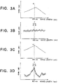
- Figs. 3A to 3D each showing a spectrum diagram of a semiconductor laser device, the Fabry-Perot problem will be described in more detail for facilitation of understanding of the present invention.
- gain of the laser device is plotted on ordinate against the wavelength of the laser plotted an abscissa.
- Fig. 3A shows a spectrum diagram for a conventional laser device of 750 ⁇ m in length having no non-current area into which current is not injected, wherein the spectrum is measured under a bias current of 0.9 times the threshold current of the laser device.
- the spectrum has a moderate mound in the vicinity of 976nm (shown as "A axis") and falls toward both sides of the mound, reflecting the gain profile of the laser active layer.
- Fig. 3B is an partially enlarged profile of Fig. 3A in the vicinity 976nm wavelength. The enlarged profile clearly shows a plurality of Fabry-Perot modes having a wavelength interval "d" of 0.18nm between the adjacent modes, which is shown as the length A-B in Fig. 3B. The wavelength interval is determined by the laser active length of 750 ⁇ m.
- FIG. 3C another spectrum diagram is shown for a conventional laser device having a total length of 800 ⁇ m and comprising a pair of non-current areas, into which current is not injected, in the vicinity of the facets of the laser device.
- Each of the non-current areas has a 25 ⁇ m length in the direction of the optical axis of the laser device, wherein the spectrum is measured under a bias current of 0.9 times the threshold current.
- the spectrum has a mound at a wavelength of 972nm roughly reflecting the gain profile of the active layer, a plurality of ripples are superimposed on the Fabry-Perot modes, such as observed in Fig. 3A.
- Fig. 3D showing an enlarged profile of Fig. 3C
- Fig. 3B in the vicinity of 972nm wavelength, a plurality of ripples are observed, which have a longer wavelength interval than the interval 0.17nm of the Fabry-Perot modes defined by the laser active length of 800 ⁇ m, in addition to the Favbry-Perot modes similar to those in Fig. 3C.
- the gain profile shifts toward the smaller wavelength, and lasing selectively at one of the Fabry-Perot modes which is nearest to the peak gain wavelength in the direction of lower wavelength.
- the wavelength interval of the hopping modes is 0.18nm which is determined by the laser active length of 750 ⁇ m.
- a semiconductor laser device having a non-current area into which current is not injected, when the injected current is increased after the start of the lasing operation, although the gain profile shifts toward the lower wavelength, lasing wavelength does not change until the peak gain wavelength approaches to the mode peak adjacent to the moderate ripple, and does change at that peak suddenly.
- the average length of the non-current area is roughly 25 ⁇ m as viewed in the direction of the optical axis of the laser device.
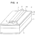
- the laser device of Fig. 4 can be fabricated as follows. First, an n-AlGaAs lower cladding layer 12, a first AlGaAs separate-confinement-heterostructure (SCH) layer not shown, an InGaAs quantum well active layer 13, a second AlGaAs SCH layer not shown, a p-AlGaAs upper cladding layer 14, and a p-GaAs contact layer 15 are consecutively formed on an n-GaAs substrate 11.
- SCH separate-confinement-heterostructure
- a ridge stripe 16 extending in the direction of the optical axis of the laser device is formed.
- top and bottom electrodes 17 and 18 were selectively deposited on the top surface and bottom surface, respectively, of the resultant wafer, followed by selectively etching the contact layer 15 of the ridge structure 16, whereby the contact layer 15 exposed from the top electrode 17 is entirely removed, to obtain the laser device 10 of Fig. 4.
- both the end surfaces 17A and 17B of the top electrode 17, as viewed in the direction of the optical axis, are slanted from the plane normal to the stripe 16 by an angle of about 10° for defining the interfaces between the current injection area, in which current is injected, and the non-current area, into which current is not injected, by the end surface 17A and 17B.
- the end surfaces 17A and 17B extend parallel to each other.
- the laser device was actually fabricated as samples which had a length of 800 ⁇ m.
- Fig. 5 the detail of the spectrum of the samples of the semiconductor laser device of Fig. 4 is shown under a bias current of 0.9 times the threshold, similarly to Figs. 3B and 3D.
- the curve of the Fabry-Perot modes is improved to be flat as compared to Fig. 4D and the moderate ripples are removed in the curve, which is due to the structure of the present embodiment wherein the boundary of the current injection area and the non-current area is slanted by about 10° from the plane normal to the stripe within the active layer.
- the wavelength interval "d" of the mode hopping after the start of the lasing operation was 0.17nm, which coincided with the interval determined by the length 800 ⁇ m of the laser device.
- the fabricated laser device exhibited a high resistance against the COD failure, and maintained the advantages of the laser device having a non-current area into which current is not injected.
- the non-current areas are formed by removing the top electrode in the vicinities of the facets of the laser device.
- the non-current areas can be formed in the present invention by other structures, such as shown in Fig. 6 which shows a modification of the first embodiment.
- the laser device of Fig. 6 is fabricated by forming a ridge stripe 16, and forming a pair of dielectric film patterns 21 on both the end portions of the ridge stripe 16, each of the film patterns 21 having a proximal end surface slanted from the plane normal to the ridge stripe 16.
- the slanted end surfaces of the dielectric film patterns 21 define the slanted interfaces 17A and 17B between the current injection area and the non-current areas.
- the top electrode may be formed on the entire surface of the ridge stripe.
- both the interfaces between the current injection area and the non-current area extend parallel to each other.
- both the interfaces need not extend parallel to each other, and may be disposed in symmetry with each other with respect to a transverse center line of the ridge stripe, as shown in the another modification of Fig. 7, or else, the interfaces may have different angle from the plane normal to the ridge stripe.
- the non-current area may be disposed at one of the facets of the ridge stripe, and preferably at the output facet of the ridge stripe.
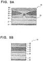
- Fig. 8 shows a top plan view of a semiconductor laser device according to a second embodiment
- Figs. 9A and 9B are sectional views taken along line A-A' and B-B', respectively, in Fig. 8.
- the laser device 30 of the present embodiment is of a buried structure having a pair of end areas in which a portion of the active layer is not formed, to obtain a window-type active layer.
- the laser device of the present embodiment is fabricated as follows. First, an n-AlGaAs lower cladding layer 32, a first SCH layer not shown, an InGaAs quantum well active layer 33, a second SCH layer not shown, a p-AlGaAs cladding layer 34, and a p-GaAs cap layer are consecutively formed or an n-GaAs substrate 31. Subsequently, layers from a top portion of the lower cladding layer 32 to the cap layer are selectively etched using a SiN mask etc, as shown in Fig.
- Samples of the semiconductor laser device of the present embodiment were fabricated and subjected to tests for the characteristics thereof.
- the samples showed the wavelength interval of the mode hopping defined by the length of the laser device, and accordingly, a stable lasing operation can be obtained, although conventional laser devices of the window type having interfaces normal to the optical axis showed larger wavelength interval of the mode hopping.
- materials for the semiconductor laser device of the present invention are not limited to the specific examples as recited above, and may be materials such as InP, GaP, GaN, and compound semiconductors containing these materials. In laser devices having either of the materials as recited above has a high resistance against a COD failure and operates in a stable lasing mode.
Landscapes
- Physics & Mathematics (AREA)
- Condensed Matter Physics & Semiconductors (AREA)
- General Physics & Mathematics (AREA)
- Electromagnetism (AREA)
- Optics & Photonics (AREA)
- Semiconductor Lasers (AREA)
Applications Claiming Priority (3)
| Application Number | Priority Date | Filing Date | Title |
|---|---|---|---|
| JP31930996 | 1996-11-29 | ||
| JP8319309A JPH10163563A (ja) | 1996-11-29 | 1996-11-29 | 半導体レーザ |
| JP319309/96 | 1996-11-29 |
Publications (3)
| Publication Number | Publication Date |
|---|---|
| EP0845841A2 true EP0845841A2 (fr) | 1998-06-03 |
| EP0845841A3 EP0845841A3 (fr) | 1999-02-17 |
| EP0845841B1 EP0845841B1 (fr) | 2003-02-26 |
Family
ID=18108764
Family Applications (1)
| Application Number | Title | Priority Date | Filing Date |
|---|---|---|---|
| EP97121320A Expired - Lifetime EP0845841B1 (fr) | 1996-11-29 | 1997-11-28 | Dispositif laser à semi-conducteur |
Country Status (3)
| Country | Link |
|---|---|
| US (1) | US5953358A (fr) |
| EP (1) | EP0845841B1 (fr) |
| JP (1) | JPH10163563A (fr) |
Cited By (2)
| Publication number | Priority date | Publication date | Assignee | Title |
|---|---|---|---|---|
| WO2002060023A1 (fr) * | 2001-01-23 | 2002-08-01 | The University Court Of The University Of Glasgow | Ameliorations apportees a des lasers a semiconducteurs |
| EP1198042A3 (fr) * | 2000-10-12 | 2004-04-28 | Fuji Photo Film Co., Ltd. | Laser à semi-conducteur avec région sans injection de courant à proximité d'une face de resonateur et son procédé de fabrication |
Families Citing this family (7)
| Publication number | Priority date | Publication date | Assignee | Title |
|---|---|---|---|---|
| RO116694B1 (ro) * | 1997-06-09 | 2001-04-30 | Iulian Basarab Petrescu-Prahova | Dispozitiv cu efect laser de tip diodă, de mare putere, şi procedeu de obţinere |
| TW413958B (en) * | 1999-07-19 | 2000-12-01 | Ind Tech Res Inst | Semiconductor laser structure |
| JP2002261379A (ja) * | 2001-03-02 | 2002-09-13 | Mitsubishi Electric Corp | 半導体デバイスおよびそれを応用した光半導体デバイス |
| US6782024B2 (en) * | 2001-05-10 | 2004-08-24 | Bookham Technology Plc | High power semiconductor laser diode |
| JP3878868B2 (ja) * | 2002-03-01 | 2007-02-07 | シャープ株式会社 | GaN系レーザ素子 |
| US7649921B2 (en) * | 2002-05-08 | 2010-01-19 | The Furukawa Electric Co., Ltd. | Laser module |
| US7687291B2 (en) | 2005-03-25 | 2010-03-30 | Trumpf Photonics Inc. | Laser facet passivation |
Family Cites Families (6)
| Publication number | Priority date | Publication date | Assignee | Title |
|---|---|---|---|---|
| JPS58141587A (ja) * | 1982-02-18 | 1983-08-22 | Toshiba Corp | 半導体レ−ザ装置 |
| US4722088A (en) * | 1984-09-14 | 1988-01-26 | Siemens Aktiengesellschaft | Semiconductor laser for high optical output power with reduced mirror heating |
| US4815084A (en) * | 1987-05-20 | 1989-03-21 | Spectra Diode Laboratories, Inc. | Semiconductor laser with integrated optical elements |
| JP3017869B2 (ja) * | 1991-12-25 | 2000-03-13 | 株式会社東芝 | 半導体光増幅器 |
| JPH07202263A (ja) * | 1993-12-28 | 1995-08-04 | Ricoh Co Ltd | 端面発光型発光ダイオード、アレイ状光源、側面受光型受光素子、受発光素子、端面発光型発光ダイオードアレイ状光源 |
| JP2944438B2 (ja) * | 1994-12-21 | 1999-09-06 | 日本電気株式会社 | 光半導体素子 |
-
1996
- 1996-11-29 JP JP8319309A patent/JPH10163563A/ja active Pending
-
1997
- 1997-11-28 EP EP97121320A patent/EP0845841B1/fr not_active Expired - Lifetime
- 1997-12-01 US US08/980,750 patent/US5953358A/en not_active Expired - Lifetime
Cited By (3)
| Publication number | Priority date | Publication date | Assignee | Title |
|---|---|---|---|---|
| EP1198042A3 (fr) * | 2000-10-12 | 2004-04-28 | Fuji Photo Film Co., Ltd. | Laser à semi-conducteur avec région sans injection de courant à proximité d'une face de resonateur et son procédé de fabrication |
| US6888866B2 (en) | 2000-10-12 | 2005-05-03 | Fuji Photo Film Co., Ltd. | Semiconductor laser device with a current non-injection region near a resonator end face, and fabrication method thereof |
| WO2002060023A1 (fr) * | 2001-01-23 | 2002-08-01 | The University Court Of The University Of Glasgow | Ameliorations apportees a des lasers a semiconducteurs |
Also Published As
| Publication number | Publication date |
|---|---|
| EP0845841B1 (fr) | 2003-02-26 |
| JPH10163563A (ja) | 1998-06-19 |
| US5953358A (en) | 1999-09-14 |
| EP0845841A3 (fr) | 1999-02-17 |
Similar Documents
| Publication | Publication Date | Title |
|---|---|---|
| CA1325670C (fr) | Lasers a semiconducteur a guide a gradient d'index et a guide a gain combines | |
| US6816527B2 (en) | Surface emitting semiconductor laser | |
| US6014396A (en) | Flared semiconductor optoelectronic device | |
| US4615032A (en) | Self-aligned rib-waveguide high power laser | |
| KR19980019159A (ko) | 반도체 레이저 | |
| US5920586A (en) | Semiconductor laser | |
| EP0845841B1 (fr) | Dispositif laser à semi-conducteur | |
| US6487225B2 (en) | Surface-emitting laser device | |
| US20040042523A1 (en) | Optically pumped semiconductor laser device | |
| EP0149563B1 (fr) | Laser à semi-conducteur | |
| KR20010007396A (ko) | 반도체 레이저 | |
| US6549553B1 (en) | Vertical-cavity surface-emitting semiconductor laser | |
| US20020136255A1 (en) | Semiconductor laser, optical element provided with the same and optical pickup provided with the optical element | |
| US7257139B2 (en) | Semiconductor laser device and optical pickup apparatus using the same | |
| US20040264532A1 (en) | Semiconductor laser diode with higher-order mode absorption layers | |
| EP0905837B1 (fr) | Dispositif laser à semiconducteur | |
| JPH0461514B2 (fr) | ||
| KR20060038057A (ko) | 반도체 레이저 소자 및 그 제조 방법 | |
| US6778573B2 (en) | Fundamental-transverse-mode index-guided semiconductor laser device having upper optical waveguide layer thinner than lower optical waveguide layer | |
| JPH1197793A (ja) | 半導体レーザ | |
| EP0284684B1 (fr) | Laser à semi-conducteur avec canal inverse et substrat plan | |
| US20070053397A1 (en) | Angled faceted emitter | |
| EP0306315B1 (fr) | Dispositif de laser semi-conducteur | |
| US20040081214A1 (en) | Narrow lateral waveguide laser | |
| US20010038657A1 (en) | Semiconductor laser device |
Legal Events
| Date | Code | Title | Description |
|---|---|---|---|
| PUAI | Public reference made under article 153(3) epc to a published international application that has entered the european phase |
Free format text: ORIGINAL CODE: 0009012 |
|
| AK | Designated contracting states |
Kind code of ref document: A2 Designated state(s): CH FR LI |
|
| AX | Request for extension of the european patent |
Free format text: AL;LT;LV;MK;RO;SI |
|
| PUAL | Search report despatched |
Free format text: ORIGINAL CODE: 0009013 |
|
| AK | Designated contracting states |
Kind code of ref document: A3 Designated state(s): AT BE CH DE DK ES FI FR GB GR IE IT LI LU MC NL PT SE |
|
| AX | Request for extension of the european patent |
Free format text: AL;LT;LV;MK;RO;SI |
|
| 17P | Request for examination filed |
Effective date: 19990728 |
|
| AKX | Designation fees paid |
Free format text: CH FR LI |
|
| REG | Reference to a national code |
Ref country code: DE Ref legal event code: 8566 |
|
| 17Q | First examination report despatched |
Effective date: 20000619 |
|
| RIC1 | Information provided on ipc code assigned before grant |
Free format text: 7H 01S 5/16 A |
|
| GRAG | Despatch of communication of intention to grant |
Free format text: ORIGINAL CODE: EPIDOS AGRA |
|
| RIC1 | Information provided on ipc code assigned before grant |
Free format text: 7H 01S 5/16 A |
|
| GRAG | Despatch of communication of intention to grant |
Free format text: ORIGINAL CODE: EPIDOS AGRA |
|
| GRAH | Despatch of communication of intention to grant a patent |
Free format text: ORIGINAL CODE: EPIDOS IGRA |
|
| GRAH | Despatch of communication of intention to grant a patent |
Free format text: ORIGINAL CODE: EPIDOS IGRA |
|
| GRAA | (expected) grant |
Free format text: ORIGINAL CODE: 0009210 |
|
| AK | Designated contracting states |
Designated state(s): CH FR LI |
|
| PG25 | Lapsed in a contracting state [announced via postgrant information from national office to epo] |
Ref country code: LI Free format text: LAPSE BECAUSE OF FAILURE TO SUBMIT A TRANSLATION OF THE DESCRIPTION OR TO PAY THE FEE WITHIN THE PRESCRIBED TIME-LIMIT Effective date: 20030226 Ref country code: FR Free format text: LAPSE BECAUSE OF NON-PAYMENT OF DUE FEES Effective date: 20030226 Ref country code: CH Free format text: LAPSE BECAUSE OF FAILURE TO SUBMIT A TRANSLATION OF THE DESCRIPTION OR TO PAY THE FEE WITHIN THE PRESCRIBED TIME-LIMIT Effective date: 20030226 |
|
| REG | Reference to a national code |
Ref country code: CH Ref legal event code: EP |
|
| PLBE | No opposition filed within time limit |
Free format text: ORIGINAL CODE: 0009261 |
|
| STAA | Information on the status of an ep patent application or granted ep patent |
Free format text: STATUS: NO OPPOSITION FILED WITHIN TIME LIMIT |
|
| EN | Fr: translation not filed | ||
| 26N | No opposition filed |
Effective date: 20031127 |