EP0845859A2 - Piezoelektrischer Resonator und elektronisches Bauelement unter Verwendung derselben Resonator - Google Patents
Piezoelektrischer Resonator und elektronisches Bauelement unter Verwendung derselben Resonator Download PDFInfo
- Publication number
- EP0845859A2 EP0845859A2 EP97105678A EP97105678A EP0845859A2 EP 0845859 A2 EP0845859 A2 EP 0845859A2 EP 97105678 A EP97105678 A EP 97105678A EP 97105678 A EP97105678 A EP 97105678A EP 0845859 A2 EP0845859 A2 EP 0845859A2
- Authority
- EP
- European Patent Office
- Prior art keywords
- base member
- resonator
- piezoelectric
- piezoelectric resonator
- electrodes
- Prior art date
- Legal status (The legal status is an assumption and is not a legal conclusion. Google has not performed a legal analysis and makes no representation as to the accuracy of the status listed.)
- Granted
Links
Images






Classifications
-
- H—ELECTRICITY
- H03—ELECTRONIC CIRCUITRY
- H03H—IMPEDANCE NETWORKS, e.g. RESONANT CIRCUITS; RESONATORS
- H03H9/00—Networks comprising electromechanical or electro-acoustic elements; Electromechanical resonators
- H03H9/15—Constructional features of resonators consisting of piezoelectric or electrostrictive material
- H03H9/17—Constructional features of resonators consisting of piezoelectric or electrostrictive material having a single resonator
- H03H9/178—Constructional features of resonators consisting of piezoelectric or electrostrictive material having a single resonator of a laminated structure of multiple piezoelectric layers with inner electrodes
-
- H—ELECTRICITY
- H03—ELECTRONIC CIRCUITRY
- H03H—IMPEDANCE NETWORKS, e.g. RESONANT CIRCUITS; RESONATORS
- H03H9/00—Networks comprising electromechanical or electro-acoustic elements; Electromechanical resonators
- H03H9/02—Details
- H03H9/02007—Details of bulk acoustic wave devices
- H03H9/02157—Dimensional parameters, e.g. ratio between two dimension parameters, length, width or thickness
-
- H—ELECTRICITY
- H03—ELECTRONIC CIRCUITRY
- H03H—IMPEDANCE NETWORKS, e.g. RESONANT CIRCUITS; RESONATORS
- H03H9/00—Networks comprising electromechanical or electro-acoustic elements; Electromechanical resonators
- H03H9/02—Details
- H03H9/05—Holders or supports
- H03H9/10—Mounting in enclosures
- H03H9/1007—Mounting in enclosures for bulk acoustic wave [BAW] devices
- H03H9/1014—Mounting in enclosures for bulk acoustic wave [BAW] devices the enclosure being defined by a frame built on a substrate and a cap, the frame having no mechanical contact with the BAW device
-
- H—ELECTRICITY
- H03—ELECTRONIC CIRCUITRY
- H03H—IMPEDANCE NETWORKS, e.g. RESONANT CIRCUITS; RESONATORS
- H03H9/00—Networks comprising electromechanical or electro-acoustic elements; Electromechanical resonators
- H03H9/46—Filters
- H03H9/54—Filters comprising resonators of piezoelectric or electrostrictive material
- H03H9/58—Multiple crystal filters
- H03H9/60—Electric coupling means therefor
- H03H9/605—Electric coupling means therefor consisting of a ladder configuration
Definitions
- the present invention relates to a piezoelectric resonator which uses the mechanical resonance of a piezoelectric member, and more particularly, to a piezoelectric resonator comprising a base member having a longitudinal direction, an active section composed of polarized piezoelectric member and constituting at least a part of the base member, and a pair of external electrodes provided with the active section.
- the present invention also relates to electronic components for use with the piezoelectric resonator, such as an oscillator, a discriminator, and a filter.
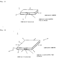
- Fig. 15 is a perspective view of a typical known type of piezoelectric resonator.
- a piezoelectric resonator generally indicated by 1 has a piezoelectric substrate 2 having, for example, a rectangularly planar shape, as viewed from the top.
- the substrate 2 is polarized in the thickness direction.
- Electrodes 3 are formed on both surfaces of the substrate 2.
- a signal is input between the electrodes 3, 3 so as to apply an electric field to the substrate 2 along its thickness, causing the substrate 2 to vibrate in the longitudinal direction.
- Fig. 16 there is shown a piezoelectric resonator 1 in which electrodes 3 are formed on both surfaces of a piezoelectric substrate 2 having a square planar shape, as viewed from the top.
- the piezoelectric substrate 2 is polarized in the thickness direction.
- a signal is input between the electrodes 3, 3 of the resonator 1 so as to apply an electric field to the substrate 2 along its thickness, thereby causing the substrate 2 to vibrate in the square-type vibration mode.
- These piezoelectric resonators 1, 1 are of an unstiffened type, in which the direction of vibration differs from the direction of polarization and the electric field.
- the electromechanical coupling coefficient of such an unstiffened piezoelectric resonator is lower than that of a stiffened piezoelectric resonator, in which the direction of vibration, the direction of polarization, and the direction in which an electric field is applied, are the same. Accordingly, an unstiffened resonator has a relatively small frequency difference ⁇ F between the resonant frequency and the anti-resonant frequency. This leads to a drawback in which a bandwidth in use is narrow when an unstiffened frequency resonator is used as a filter of an oscillator. Thus, flexibility in designing the characteristics is low in the above type of piezoelectric resonator and electronic components using such a resonator.
- the piezoelectric resonator 1 shown in Fig. 15 utilizes the first-order (basic) resonance in the longitudinal mode. At the same time, however, the resonator 1 also generates due to its structure large spurious resonances in the odd-number-order higher harmonic modes, such as the third-order and fifth-order modes, and in the width mode. Some measures to suppress these spurious resonances may be considered, such as polishing, increasing mass, and changing the shape of the electrode. These measures, however, increase the manufacturing cost. Additionally, since the piezoelectric substrate is formed in a rectangular planar shape as viewed from the top, the substrate cannot be made too thin due to restrictions in strength. Accordingly, the distance between the electrodes cannot be reduced and a capacitance between terminals cannot be made large.
- this type of resonator needs a large size as compared with a piezoelectric resonator using longitudinal vibration in order to obtain the same resonant frequency, it is difficult to reduce the size of the former type of resonator.
- the resonators connected in series are made thick, and electrodes are formed only on part of a piezoelectric substrate to decrease the capacitance as well. In this case, since the electrodes are only partially formed, not only the capacitance, but also the difference ⁇ F between the resonant frequency and the anti-resonant frequency, are reduced.
- the resonators connected in parallel are accordingly required to have a small frequency difference ⁇ F.
- the piezoelectricity of the piezoelectric substrate cannot be effectively used, and the pass bandwidth of the filter cannot be increased.
- a laminated piezoelectric resonator was proposed by the present inventor, for example, in Japanese Patent Application No. 8-122725. This resonator is a stiffened type, in which the direction of vibration and the direction in which an electric field is applied are the same.
- the resonator has more factors that contribute to filter characteristics, such as the width and thickness of the resonator, and the number of laminated layers used in the resonator, as compared with a known type of piezoelectric resonator formed of only a single substrate. Then, an examination was made whether good filter characteristics would be obtained by adjusting the above-described factors when this type of laminated piezoelectric resonator is applied to an electronic component, such as a ladder filter. Through this study it was revealed that the frequency difference ⁇ F is seriously decreased, and spurious resonances are increased, depending on the dimensions, such as the length, width and thickness, of the resonator. This further proves that the determination of the dimensions of the resonator is an important factor.
- the present invention provides a piezoelectric resonator of the above mentioned kind, which is characterized in that at least one pair of internal electrodes disposed in the active section such that the internal electrodes are perpendicular to the longitudinal direction of the base member and are connected to the pair of external electrodes respectively, the active section is polarized in the longitudinal direction of the base member, said base member excites a longitudinal mode basic vibration when an electric field is applied to the longitudinal direction of the base member via the internal electrodes, and the piezoelectric resonator has a rectangular planar shape viewed from the top thereof, and satisfies the conditions of L ⁇ 2W and L ⁇ 2T when L, W, T indicate the length, width, and thickness of said piezoelectric resonator, respectively.
- ends of the internal electrodes may be exposed at a side face of the base member, a first insulating film may be provided to cover exposed portions of internal electrodes among the internal electrodes at one end of the side face of the base member, a second insulating film may be provided to cover exposed portions of internal electrodes among the internal electrodes which are not covered by the first insulating film at the other end of the side face of the base member, the pair of external electrodes may be respectively extended in the longitudinal direction at said one and the other ends of the side face of the base member and connected to said internal electrodes which are not covered by said first and second insulating films at each end of the side face of said base member.
- ends of the internal electrodes may be partially exposed at a side face of the base member such that the exposed portions of the internal electrodes adjacent to each other are electrically connected to the pair of external electrodes respectively.
- an inactive section in which vibration is not excited when the electric field is applied, may constitute the other part of the base member.
- a support member may be provided at a center of the base member in the longitudinal direction.
- This invention also provides an electronic component for use with the above described piezoelectric resonator, which is characterized in that the support member is provided on a insulating substrate, and a pattern electrode is provided on the insulating substrate and connected to the external electrodes of the piezoelectric resonator.
- the above described electronic component may be a ladder filter in which the plurality of pattern electrodes are provided on the insulating substrate and connected to the external electrodes of the plurality of piezoelectric resonators such that the piezoelectric resonators are connected each other in a ladder shape.
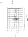
- ⁇ F/F a is increased (a difference between the resonant frequency and the anti-resonant frequency, ⁇ F, is increased), and spurious resonances are decreased.
- Fig. 4 shows that ⁇ F/F a is sharply decreased if L is smaller than two times W i.e., L/W ⁇ 2.
- Fig. 5 indicates that ⁇ F/F a sharply drops if L is smaller than two times T i.e., L/T ⁇ 2.
- the capacitance of the resonator is adjustable, it is easy to achieve impedance matching with an external circuit in a case when the resonator is mounted on, for example, a circuit board.
- ⁇ F and the capacitance are adjustable, and thus, a piezoelectric resonator having high flexibility in designing the characteristics and an electronic component for use with such a resonator can be provided.
- an electronic component such as a filter, a discriminator, or an oscillator using the above type of piezoelectric resonator can be produced by the following process.
- the resonator is mounted on a support substrate on which pattern electrodes are formed, and preferably the resonator is then covered with a cap.
- a chip-type electronic component can be completed.
- the resonator can be mounted on the pattern electrodes disposed on the support substrate without needing to use a lead wire by virtue of the face bonding structure.
- support members have been formed at the center of the base member, and thus, the node of the resonator can be positively supported when the resonator is mounted on the pattern electrodes.
- an electronic component using this resonator can be produced with reduced cost because the resonator can be connected via support members to the pattern electrodes formed on a support substrate without needing to use a lead wire.
- the support members have been provided for the piezoelectric resonator, so that vibrations of the resonator are not impeded, thereby obtaining piezoelectric components having good characteristics.
- a ladder filter exhibiting good characteristics can be produced with reduced cost. Since a chip-type electronic component can be made by the use of the above piezoelectric resonator, it can be readily mounted on a circuit board.
- the capacitance can be regulated by constructing the resonator with a laminated structure, and it is easy to achieve impedance matching between such a component and an external circuit.
- a piezoelectric resonator generally designated by 10 formed in a rectangular planar shape as viewed from the top, has a base member 12 formed, for example, in a rectangular-prism shape.
- the base member 12 is made from, for example, a piezoelectric ceramic material.
- a plurality of internal electrodes 14 are formed in the base member 12 in such a manner that the surfaces of the electrodes 14 are perpendicular to a longitudinal direction of the base member 12.
- the base member 12 is longitudinally polarized so that the directions of polarization are opposite to each other at both ends of one electrode 14, as indicated by the arrows in Fig. 2.
- the dimensions of the base member 12 are determined in the following manner. When the length, width, and thickness of the base member 12 are indicated by L, W and T, respectively, the dimensions of the base member 12 are set to satisfy the conditions of L 3 2W and L 3 2T. Namely, the dimensions of the base member 12 are formed to satisfy the conditions of L/W 3 2 and L/T 3 2. Formed on one lateral surface of the base member 12 is a groove 15 extending in the longitudinal direction of the base member 12.
- the groove 15 is formed in the central portion of the base member 12 in a widthwise direction so as to divide one lateral surface of the base member 12 into two portions. Further, a first insulating film 16 and a second insulating film 18 are provided, as illustrated in Fig. 3, for the lateral surface divided by the groove 15. On one side face of the divided lateral surface of the base member 12, the first insulating film 16 covers the exposed sections of every other electrode 14. On the other side face of the base member 12, the second insulating film 18 covers the exposed sections of every other electrode 14 which are not covered by the first insulating film 16. It should be noted that both ends of the base member 12 are not polarized.
- external electrodes 20 and 22 are disposed on the lateral surface on which the first and second insulating films 16 and 18 are formed, i.e., on both sides of the groove 15.
- the electrode 20 is connected to the internal electrodes 14 which are not covered with the first insulating film 16, while the electrode 22 is connected to the internal electrodes 14 which are not covered with the second insulating film 18.
- two adjacent electrodes 14 are connected to the external electrodes 20 and 22, respectively.
- the exposed sections of the internal electrodes 14 are covered with the first and second insulating films 16 and 18, and the external electrodes 20 and 22 are further formed on the films 16 and 18, respectively.
- the base member 12 is not necessarily grooved, as illustrated in Fig. 1B.
- the insulating films 16 and 18 may alternately cover the exposed sections of the internal electrodes 14 at both ends of the base member 12 in the widthwise direction, and the external electrodes 20 and 22 may be disposed in two rows to extend along the base member 12 in the longitudinal direction.
- the base member 12 is not grooved, adjacent internal electrodes 14 are connected to the external electrodes 20 and 22, respectively.
- the internal electrodes 14 may be configured such that only part of the electrodes 14 connected to the external electrodes 20 and 22 may be exposed from the surface of a laminated block of the piezoelectric resonator 10, and the other portions may not be exposed.
- the above-constructed resonator 10 uses the external electrodes 20 and 22 as input and output electrodes.
- the base member 12 except for both the ends, becomes piezoelectrically active because an electric field is applied between adjacent internal electrodes 14.
- the member 12 is, however, piezoelectrically inactive at both the ends because it is not polarized therein and also because an electric field is not applied because of the absence of electrodes.
- an active section 26, which is responsive to input signals is formed at the center of the base member 12 while inactive sections 28, which is unresponsive to input signals, are formed at both ends of the member 12.
- the inactive sections 28 do not generate driving force by input signals.
- an electric field may be applied between the internal electrodes 14 as long as they are not polarized.
- the inactive portions 28 may be constructed in such a manner that the piezoelectric layers may be polarized as long as an electric field is not applied.
- a signal is input to the external electrodes 20 and 22 so as to apply opposite voltages to the piezoelectric layers of the active section 26 polarized in the opposite directions. This causes the piezoelectric layers to expand and contract in the same direction as a whole.
- the overall piezoelectric resonator 10 vibrates in the longitudinal direction in the basic mode in which the center of the base member 12 serves as a node.
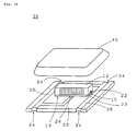
- an electronic component generally indicated by 30 has an insulating substrate 32. At each of the opposing end portions of the substrate 32, two indentations 34 are formed. Disposed on one surface of the substrate 32 are two pattern electrodes 36 and 38. One pattern electrode 36 is formed between opposing indentations 34 and extends in an L" shape from a point near one end of the electrode 36 toward the center of the substrate 32.
- the other electrode 38 is disposed between the other opposing indentations 34 and extends in an L" shape from a point near one end of the electrode 38 (opposite to the one end of the electrode 36) toward the center of the substrate 32.
- the pattern electrodes 36 and 38 are disposed to opposedly face each other with a spacing.
- the electrodes 36 and 38 are formed to be routed in a roundabout fashion from the ends of the substrate 32 to the reverse surface of the substrate 32.
- the piezoelectric resonator 10 is mounted on the insulating substrate 32 by support members 24.
- the support members 24 are formed at the central portions of the respective external electrodes 20 and 22 in the longitudinal direction.
- the support members 24 are formed so that they can become conductive.
- the support members 24 may be made from a conductive material, such as conductive adhesive. Alternatively, an insulator coated with an electrode film may adhere to each of the external electrodes 20 and 22 through a conductive material. Then, the support members 24 formed as noted above are, as illustrated in Fig. 11, connected through, for example, conductive adhesive (not shown), to the ends of the respective pattern electrodes 36 and 38 disposed at the center of the substrate 32. Thus, the external electrodes 20 and 22 of the resonator 10 can be securely mounted on the insulating substrate 32 and also electrically connected to the pattern electrodes 36 and 38, respectively. Referring back to Fig. 10, a metallic cap 40 is placed on the substrate 32 to complete the electronic component 30.
- a metallic cap 40 is placed on the substrate 32 to complete the electronic component 30.
- insulating resin is applied to the insulating substrate 32 and the pattern electrodes 36 and 38 in advance.
- the pattern electrodes 36 and 38 which are formed to be routed in a roundabout manner from the ends of the substrate 32 to the reverse surface of the substrate 32, are used as input and output terminals for connecting the resonator 10 to external circuits.
- the dimensions of the piezoelectric resonator 10 are determined to satisfy the conditions of L 3 2W and L 3 2T. Accordingly, a difference between the resonant frequency and the anti-resonant frequency, i.e., ⁇ F, can be increased. Thus, in this electronic component 30, a large frequency difference ⁇ F/F a and small spurious resonances can be achieved. Also, in this component 30, since the piezoelectric resonator 10 is held by the support members 24 formed at the central portion of the longitudinal substrate 12, the ends of the resonator 10 can be disposed separately from the substrate 32, so that vibrations are not impeded.
- the central portion of the resonator 10, which serves as a node, can be secured by the support members 24, and the external electrodes 20 and 22 are electrically connected to the pattern electrodes 36 and 38, respectively. Since the support members 24 have been formed on the resonator 10, they can be correctly positioned to the node of the resonator 10. Thus, the node can be supported more correctly by the support members 24 arranged as described above as compared with, for example, the following arrangement of support members. That is, support members in the form of, for example, projections, are formed on the pattern electrodes 36 and 38, and the piezoelectric resonator 10 is mounted on the support members. As a consequence, vibration leakage of the resonator 10 can be avoided, thereby obtaining good characteristics.
- the electronic component 30 can be manufactured with reduced cost.
- the electronic component 30, together with IC chips, can be mounted on a substrate to form an oscillator or a discriminator. Since the electronic component 30 constructed as described above is sealed and protected by the metallic cap 40, it can be used as a chip-type (surface mount) component which is mountable by reflow soldering.
- this electronic component 30 using the above type of resonator 10 is employed in an oscillator, spurious vibrations can be suppressed to a low level, which would otherwise cause unusual vibrations. It is also easy to achieve impedance matching with an external circuit since any desired level of capacitance can be set. Particularly when the electronic component 30 is used in an oscillator for voltage-controlled oscillation, a wide frequency variable range can be obtained due to a large frequency difference ⁇ F, which cannot be conventionally accomplished. Moreover, when this electronic component 30 is used in a discriminator, a wide peak-separation range can be provided due to a large ⁇ F of the resonator.
- a ladder filter may be produced using a plurality of piezoelectric resonators 10.
- Fig. 12 is a plan view of the essential portion of an electronic component used as a ladder filter having a ladder-shaped circuit.
- Fig. 13 is an exploded perspective view of the electronic component shown in Fig. 12.
- an electronic component generally designated by 50 shown in Fig. 13 four pattern electrodes 56, 58, 60 and 62 are formed on an insulating substrate 52. Five lands are provided for these pattern electrodes 56 through 62 in such a manner that they are disposed in a row with intervals.
- the first land from one end of the substrate 52 is provided for the pattern electrodes 56; the second and fifth lands are formed at the electrode 58; the third land is disposed at the electrode 60; and the fourth land is provided for the electrode 62.
- Fixed to these lands are support members 24 mounted on the external electrodes 20 and 22 of the individual piezoelectric resonators 10a, 10b, 10c and 10d.
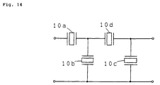
- the resonators 10a through 10d are mounted on the substrate 52 in such a manner that the ladder-shaped circuit illustrated in Fig. 14 can be obtained.
- a metallic cap (not shown) is placed on the substrate 52.
- the electronic component 50 constructed as described above can thus be used as a ladder filter having a ladder-shaped circuit shown in Fig. 14.
- Two resonators 10a and 10d may be used as series piezoelectric resonators, while the other two resonators 10b and 10c may serve as parallel piezoelectric resonators.
- This type of ladder filter is designed so that the capacitance of the parallel resonators 10b and 10c is much larger than the capacitance of the series resonators 10a and 10d. Attenuation in the ladder filter is determined by the capacitance ratio between the series resonators and the parallel resonators.
- L, W and T the lengths, widths, and thicknesses of the resonators 10a through 10d are represented by L, W and T, respectively, this electronic component 50, as well as the previous electronic component 30, is designed to satisfy the conditions of L ⁇ 2W and L ⁇ 2T.
- the frequency difference ⁇ F can be increased.
- the electronic component 50 can exhibit large ⁇ F/F a and small spurious resonances.
- the capacitance can be adjusted by changing the number of laminated layers used in the piezoelectric resonators 10a through 10d.
- a ladder filter having a larger attenuation with fewer piezoelectric resonators can be implemented by changing the capacitance of the resonators 10a through 10d, as compared with a case where conventional unstiffened piezoelectric resonators are employed.
- the resonators 10a through 10d have a larger ⁇ F than known piezoelectric resonators, a wider pass bandwidth of a resulting ladder filter can be achieved as compared with a filter using conventional resonators.
- the dimensions of the resonator 10 are determined, in particular, to satisfy the conditions of L ⁇ 2W and L ⁇ 2T. Accordingly, the characteristics of the resonator 10, such as the capacitance, can be regulated. As a consequence, a resonator 10 having a high level of flexibility in designing the characteristics can be obtained.
- the electronic components 30 and 50 using the resonator 10 can be attained.
Landscapes
- Physics & Mathematics (AREA)
- Acoustics & Sound (AREA)
- Chemical & Material Sciences (AREA)
- Crystallography & Structural Chemistry (AREA)
- Piezo-Electric Or Mechanical Vibrators, Or Delay Or Filter Circuits (AREA)
Applications Claiming Priority (4)
| Application Number | Priority Date | Filing Date | Title |
|---|---|---|---|
| JP334521/96 | 1996-11-28 | ||
| JP33452196A JP3271538B2 (ja) | 1996-11-28 | 1996-11-28 | 圧電共振子およびそれを用いた電子部品 |
| JP33452196 | 1996-11-28 | ||
| US08/846,295 US5962956A (en) | 1996-11-28 | 1997-04-30 | Piezoelectric resonator and electronic component containing same |
Publications (3)
| Publication Number | Publication Date |
|---|---|
| EP0845859A2 true EP0845859A2 (de) | 1998-06-03 |
| EP0845859A3 EP0845859A3 (de) | 1998-09-02 |
| EP0845859B1 EP0845859B1 (de) | 2002-07-31 |
Family
ID=26574862
Family Applications (1)
| Application Number | Title | Priority Date | Filing Date |
|---|---|---|---|
| EP97105678A Expired - Lifetime EP0845859B1 (de) | 1996-11-28 | 1997-04-07 | Piezoelektrischer Resonator und elektronisches Bauelement unter Verwendung derselben Resonator |
Country Status (5)
| Country | Link |
|---|---|
| US (1) | US5962956A (de) |
| EP (1) | EP0845859B1 (de) |
| JP (1) | JP3271538B2 (de) |
| CN (1) | CN1100383C (de) |
| NO (1) | NO971936L (de) |
Cited By (1)
| Publication number | Priority date | Publication date | Assignee | Title |
|---|---|---|---|---|
| EP0874456B1 (de) * | 1997-04-25 | 2004-04-07 | Murata Manufacturing Co., Ltd. | Piezoelektrischer Resonator und elektronisches Bauteil damit |
Families Citing this family (2)
| Publication number | Priority date | Publication date | Assignee | Title |
|---|---|---|---|---|
| JP3399415B2 (ja) * | 1999-09-27 | 2003-04-21 | 株式会社村田製作所 | センサアレイ、センサアレイの製造方法および超音波診断装置 |
| JP3538709B2 (ja) | 2000-06-14 | 2004-06-14 | 株式会社村田製作所 | 圧電共振部品 |
Family Cites Families (55)
| Publication number | Priority date | Publication date | Assignee | Title |
|---|---|---|---|---|
| US2157665A (en) * | 1935-10-16 | 1939-05-09 | Telefunken Gmbh | Crystal mounting with temperature compensation |
| US2998535A (en) * | 1958-04-29 | 1961-08-29 | Acoustica Associates Inc | Composite electro-acoustic transducer configuration |
| US3187207A (en) * | 1960-08-08 | 1965-06-01 | Giannini Controls Corp | Transducers |
| US3185869A (en) * | 1961-12-01 | 1965-05-25 | Endevco Corp | Transducer |
| US3297889A (en) * | 1964-01-15 | 1967-01-10 | Breskend Sam | Clock driver |
| CH429228A (de) * | 1964-12-10 | 1967-01-31 | Kistler Instrumente Ag | Piezoelektrischer Einbaukörper zum Einbau in einen piezoelektrischen Wandler |
| US3378704A (en) * | 1966-01-05 | 1968-04-16 | Bourns Inc | Piezoelectric multilayer device |
| US3401275A (en) * | 1966-04-14 | 1968-09-10 | Clevite Corp | Composite resonator |
| GB1207974A (en) * | 1966-11-17 | 1970-10-07 | Clevite Corp | Frequency selective apparatus including a piezoelectric device |
| CH607336A5 (de) * | 1975-09-22 | 1978-12-15 | Siemens Ag | |
| US4193009A (en) * | 1976-01-26 | 1980-03-11 | Durley Benton A Iii | Ultrasonic piezoelectric transducer using a rubber mounting |
| GB2044527B (en) * | 1978-12-27 | 1983-05-25 | Murata Manufacturing Co | Piezoelectric unit and device |
| US4398117A (en) * | 1981-03-23 | 1983-08-09 | Sperry Corporation | Bellows support for surface acoustic wave device |
| JPS59117814A (ja) * | 1982-12-24 | 1984-07-07 | Murata Mfg Co Ltd | 圧電磁器共振子 |
| US4532451A (en) * | 1982-12-28 | 1985-07-30 | Murata Manufacturing Co., Ltd. | Terminals and mounting for piezoelectric resonators |
| JPS601877A (ja) * | 1983-06-20 | 1985-01-08 | Nippon Soken Inc | 積層型圧電体 |
| US4564782A (en) * | 1983-09-02 | 1986-01-14 | Murata Manufacturing Co., Ltd. | Ceramic filter using multiple thin piezoelectric layers |
| JPS6074709A (ja) * | 1983-09-29 | 1985-04-27 | Murata Mfg Co Ltd | 圧電装置 |
| JPS6086880A (ja) * | 1983-10-19 | 1985-05-16 | Nec Corp | 電歪効果素子 |
| JPS60124108A (ja) * | 1983-12-08 | 1985-07-03 | Murata Mfg Co Ltd | 圧電共振子および圧電共振部品 |
| JPS60169927U (ja) * | 1984-04-17 | 1985-11-11 | 株式会社村田製作所 | ラダ−型フイルタ |
| JPS60174312U (ja) * | 1984-04-27 | 1985-11-19 | 京セラ株式会社 | 水晶発振器 |
| US4542315A (en) * | 1984-05-15 | 1985-09-17 | Murata Manufacturing Co., Ltd. | Chip-shaped piezoelectric vibrator mount |
| JPS61133715A (ja) * | 1984-12-03 | 1986-06-21 | Murata Mfg Co Ltd | 周波数調整可能な圧電素子 |
| JPS61139112A (ja) * | 1984-12-10 | 1986-06-26 | Murata Mfg Co Ltd | 周波数調整可能な積層型圧電素子 |
| US4752712A (en) * | 1985-06-10 | 1988-06-21 | Nippon Soken, Inc. | Piezoelectric laminate stack |
| US4885498A (en) * | 1985-06-19 | 1989-12-05 | Ngk Spark Plug Co., Ltd. | Stacked type piezoelectric actuator |
| JPH0732273B2 (ja) * | 1986-05-22 | 1995-04-10 | 日本電気株式会社 | 電歪効果素子 |
| US5045744A (en) * | 1988-12-23 | 1991-09-03 | Murata Mfg. Co. | Energy-trapping-by-frequency-lowering-type piezoelectric-resonance device |
| US5118982A (en) * | 1989-05-31 | 1992-06-02 | Nec Corporation | Thickness mode vibration piezoelectric transformer |
| JP3041952B2 (ja) * | 1990-02-23 | 2000-05-15 | セイコーエプソン株式会社 | インクジェット式記録ヘッド、圧電振動体、及びこれらの製造方法 |
| JP2965602B2 (ja) * | 1990-02-26 | 1999-10-18 | 日立金属株式会社 | 積層型変位素子 |
| US5126618A (en) * | 1990-03-06 | 1992-06-30 | Brother Kogyo Kabushiki Kaisha | Longitudinal-effect type laminar piezoelectric/electrostrictive driver, and printing actuator using the driver |
| JPH04214686A (ja) * | 1990-10-05 | 1992-08-05 | Nec Corp | 電歪効果素子 |
| DE4201937C2 (de) * | 1991-01-25 | 1997-05-22 | Murata Manufacturing Co | Piezoelektrisches laminiertes Stellglied |
| JP3185226B2 (ja) * | 1991-01-30 | 2001-07-09 | 株式会社村田製作所 | 圧電バイモルフ素子の駆動方法及び圧電バイモルフ素子 |
| JP3064458B2 (ja) * | 1991-04-02 | 2000-07-12 | 日本電気株式会社 | 厚み縦振動圧電磁器トランスとその駆動方法 |
| JPH04333295A (ja) * | 1991-05-09 | 1992-11-20 | Nec Corp | 電歪効果素子およびその製造方法 |
| US5225731A (en) * | 1991-06-13 | 1993-07-06 | Southwest Research Institute | Solid body piezoelectric bender transducer |
| JPH05160459A (ja) * | 1991-12-09 | 1993-06-25 | Hitachi Metals Ltd | 積層型変位素子 |
| JPH05264391A (ja) * | 1992-03-19 | 1993-10-12 | Unisia Jecs Corp | 圧力センサ |
| US5250870A (en) * | 1992-03-25 | 1993-10-05 | Motorola, Inc. | Ultra-thin surface mount crystal package |
| JPH06209228A (ja) * | 1993-01-12 | 1994-07-26 | Murata Mfg Co Ltd | ラダー型フィルタ |
| US5381067A (en) * | 1993-03-10 | 1995-01-10 | Hewlett-Packard Company | Electrical impedance normalization for an ultrasonic transducer array |
| US5648746A (en) * | 1993-08-17 | 1997-07-15 | Murata Manufacturing Co., Ltd. | Stacked diezoelectric resonator ladder-type filter with at least one width expansion mode resonator |
| JPH07106905A (ja) * | 1993-10-06 | 1995-04-21 | Matsushita Electric Ind Co Ltd | 発振子 |
| US5585687A (en) * | 1994-02-23 | 1996-12-17 | Citizen Watch Co., Ltd. | Piezolelectric oscillator |
| JPH07240660A (ja) * | 1994-02-25 | 1995-09-12 | Murata Mfg Co Ltd | ラダー型フィルタ |
| JPH0818382A (ja) * | 1994-06-27 | 1996-01-19 | Murata Mfg Co Ltd | 圧電部品 |
| JP3221253B2 (ja) * | 1994-09-13 | 2001-10-22 | 株式会社村田製作所 | 複合電子部品の製造方法 |
| JP3114526B2 (ja) * | 1994-10-17 | 2000-12-04 | 株式会社村田製作所 | チップ型圧電共振部品 |
| US5572082A (en) * | 1994-11-14 | 1996-11-05 | Sokol; Thomas J. | Monolithic crystal strip filter |
| JP2986706B2 (ja) * | 1995-03-03 | 1999-12-06 | 日立金属株式会社 | 圧電素子及びそれを用いた圧電アクチュエータ |
| JP3141723B2 (ja) * | 1995-04-11 | 2001-03-05 | 株式会社村田製作所 | 幅モードを利用した共振子及び共振部品 |
| JP3271517B2 (ja) * | 1996-04-05 | 2002-04-02 | 株式会社村田製作所 | 圧電共振子およびそれを用いた電子部品 |
-
1996
- 1996-11-28 JP JP33452196A patent/JP3271538B2/ja not_active Expired - Lifetime
-
1997
- 1997-04-07 EP EP97105678A patent/EP0845859B1/de not_active Expired - Lifetime
- 1997-04-25 NO NO971936A patent/NO971936L/no not_active Application Discontinuation
- 1997-04-28 CN CN97110878A patent/CN1100383C/zh not_active Expired - Lifetime
- 1997-04-30 US US08/846,295 patent/US5962956A/en not_active Expired - Lifetime
Cited By (1)
| Publication number | Priority date | Publication date | Assignee | Title |
|---|---|---|---|---|
| EP0874456B1 (de) * | 1997-04-25 | 2004-04-07 | Murata Manufacturing Co., Ltd. | Piezoelektrischer Resonator und elektronisches Bauteil damit |
Also Published As
| Publication number | Publication date |
|---|---|
| NO971936L (no) | 1998-05-29 |
| CN1100383C (zh) | 2003-01-29 |
| CN1184377A (zh) | 1998-06-10 |
| NO971936D0 (no) | 1997-04-25 |
| EP0845859B1 (de) | 2002-07-31 |
| US5962956A (en) | 1999-10-05 |
| JPH10163794A (ja) | 1998-06-19 |
| JP3271538B2 (ja) | 2002-04-02 |
| EP0845859A3 (de) | 1998-09-02 |
Similar Documents
| Publication | Publication Date | Title |
|---|---|---|
| EP0823781B1 (de) | Piezoelektrischer Resonator, Verfahren zu seiner Herstellung, und elektronisches Bauelement mit diesem Resonator | |
| EP0800269B1 (de) | Piezoelektrischer Resonator und elektronisches Bauelement unter Verwendung derselben | |
| US5892416A (en) | Piezoelectric resonator and electronic component containing same | |
| EP0829957B1 (de) | Piezoelektrischer Resonator und elektronisches Bauelement damit | |
| EP0820144B1 (de) | Piezoelektrischer Resonator und elektrisches Bauteil unter Verwendung derselben | |
| EP0827273B1 (de) | Piezoelektrischer Resonator und elektronisches Bauteil mit diesem Resonator | |
| EP0845859B1 (de) | Piezoelektrischer Resonator und elektronisches Bauelement unter Verwendung derselben Resonator | |
| EP0874456B1 (de) | Piezoelektrischer Resonator und elektronisches Bauteil damit | |
| KR100280072B1 (ko) | 압전공진자및이를구비한전자부품 | |
| JP3262050B2 (ja) | 電子部品およびラダーフィルタ | |
| JP3271541B2 (ja) | 圧電共振子およびそれを用いた電子部品 | |
| EP0800268B1 (de) | Piezoelektrischer Resonator | |
| KR100301717B1 (ko) | 전자부품및래더필터 | |
| JP3262021B2 (ja) | 圧電共振子およびそれを用いた電子部品 | |
| JP2000165181A (ja) | 圧電共振子、電子部品および通信機器 | |
| JPH10303694A (ja) | 圧電共振子およびそれを用いた電子部品 | |
| JPH10107577A (ja) | 電子部品およびラダーフィルタ | |
| JPH11168347A (ja) | 圧電共振子、電子部品および通信機器 |
Legal Events
| Date | Code | Title | Description |
|---|---|---|---|
| PUAI | Public reference made under article 153(3) epc to a published international application that has entered the european phase |
Free format text: ORIGINAL CODE: 0009012 |
|
| AK | Designated contracting states |
Kind code of ref document: A2 Designated state(s): DE FI FR SE |
|
| PUAL | Search report despatched |
Free format text: ORIGINAL CODE: 0009013 |
|
| AK | Designated contracting states |
Kind code of ref document: A3 Designated state(s): AT BE CH DE DK ES FI FR GB GR IE IT LI LU MC NL PT SE |
|
| 17P | Request for examination filed |
Effective date: 19981217 |
|
| AKX | Designation fees paid |
Free format text: DE FI FR SE |
|
| RBV | Designated contracting states (corrected) |
Designated state(s): DE FI FR SE |
|
| GRAG | Despatch of communication of intention to grant |
Free format text: ORIGINAL CODE: EPIDOS AGRA |
|
| GRAG | Despatch of communication of intention to grant |
Free format text: ORIGINAL CODE: EPIDOS AGRA |
|
| GRAH | Despatch of communication of intention to grant a patent |
Free format text: ORIGINAL CODE: EPIDOS IGRA |
|
| 17Q | First examination report despatched |
Effective date: 20010905 |
|
| GRAH | Despatch of communication of intention to grant a patent |
Free format text: ORIGINAL CODE: EPIDOS IGRA |
|
| GRAA | (expected) grant |
Free format text: ORIGINAL CODE: 0009210 |
|
| AK | Designated contracting states |
Kind code of ref document: B1 Designated state(s): DE FI FR SE |
|
| PG25 | Lapsed in a contracting state [announced via postgrant information from national office to epo] |
Ref country code: FI Free format text: LAPSE BECAUSE OF FAILURE TO SUBMIT A TRANSLATION OF THE DESCRIPTION OR TO PAY THE FEE WITHIN THE PRESCRIBED TIME-LIMIT Effective date: 20020731 |
|
| REF | Corresponds to: |
Ref document number: 69714389 Country of ref document: DE Date of ref document: 20020905 |
|
| PG25 | Lapsed in a contracting state [announced via postgrant information from national office to epo] |
Ref country code: SE Free format text: LAPSE BECAUSE OF FAILURE TO SUBMIT A TRANSLATION OF THE DESCRIPTION OR TO PAY THE FEE WITHIN THE PRESCRIBED TIME-LIMIT Effective date: 20021031 |
|
| ET | Fr: translation filed | ||
| PLBE | No opposition filed within time limit |
Free format text: ORIGINAL CODE: 0009261 |
|
| STAA | Information on the status of an ep patent application or granted ep patent |
Free format text: STATUS: NO OPPOSITION FILED WITHIN TIME LIMIT |
|
| 26N | No opposition filed |
Effective date: 20030506 |
|
| REG | Reference to a national code |
Ref country code: FR Ref legal event code: PLFP Year of fee payment: 20 |
|
| PGFP | Annual fee paid to national office [announced via postgrant information from national office to epo] |
Ref country code: DE Payment date: 20160421 Year of fee payment: 20 |
|
| PGFP | Annual fee paid to national office [announced via postgrant information from national office to epo] |
Ref country code: FR Payment date: 20160421 Year of fee payment: 20 |
|
| REG | Reference to a national code |
Ref country code: DE Ref legal event code: R071 Ref document number: 69714389 Country of ref document: DE |