EP0847049A2 - Support d'enregistrement d'information optique - Google Patents
Support d'enregistrement d'information optique Download PDFInfo
- Publication number
- EP0847049A2 EP0847049A2 EP97109498A EP97109498A EP0847049A2 EP 0847049 A2 EP0847049 A2 EP 0847049A2 EP 97109498 A EP97109498 A EP 97109498A EP 97109498 A EP97109498 A EP 97109498A EP 0847049 A2 EP0847049 A2 EP 0847049A2
- Authority
- EP
- European Patent Office
- Prior art keywords
- layer
- optical information
- thickness
- recording
- recording medium
- Prior art date
- Legal status (The legal status is an assumption and is not a legal conclusion. Google has not performed a legal analysis and makes no representation as to the accuracy of the status listed.)
- Withdrawn
Links
Images


Classifications
-
- G—PHYSICS
- G11—INFORMATION STORAGE
- G11B—INFORMATION STORAGE BASED ON RELATIVE MOVEMENT BETWEEN RECORD CARRIER AND TRANSDUCER
- G11B7/00—Recording or reproducing by optical means, e.g. recording using a thermal beam of optical radiation by modifying optical properties or the physical structure, reproducing using an optical beam at lower power by sensing optical properties; Record carriers therefor
- G11B7/24—Record carriers characterised by shape, structure or physical properties, or by the selection of the material
- G11B7/241—Record carriers characterised by shape, structure or physical properties, or by the selection of the material characterised by the selection of the material
- G11B7/252—Record carriers characterised by shape, structure or physical properties, or by the selection of the material characterised by the selection of the material of layers other than recording layers
- G11B7/257—Record carriers characterised by shape, structure or physical properties, or by the selection of the material characterised by the selection of the material of layers other than recording layers of layers having properties involved in recording or reproduction, e.g. optical interference layers or sensitising layers or dielectric layers, which are protecting the recording layers
- G11B7/2578—Record carriers characterised by shape, structure or physical properties, or by the selection of the material characterised by the selection of the material of layers other than recording layers of layers having properties involved in recording or reproduction, e.g. optical interference layers or sensitising layers or dielectric layers, which are protecting the recording layers consisting essentially of inorganic materials
-
- G—PHYSICS
- G11—INFORMATION STORAGE
- G11B—INFORMATION STORAGE BASED ON RELATIVE MOVEMENT BETWEEN RECORD CARRIER AND TRANSDUCER
- G11B7/00—Recording or reproducing by optical means, e.g. recording using a thermal beam of optical radiation by modifying optical properties or the physical structure, reproducing using an optical beam at lower power by sensing optical properties; Record carriers therefor
- G11B7/004—Recording, reproducing or erasing methods; Read, write or erase circuits therefor
- G11B7/006—Overwriting
- G11B7/0062—Overwriting strategies, e.g. recording pulse sequences with erasing level used for phase-change media
-
- G—PHYSICS
- G11—INFORMATION STORAGE
- G11B—INFORMATION STORAGE BASED ON RELATIVE MOVEMENT BETWEEN RECORD CARRIER AND TRANSDUCER
- G11B7/00—Recording or reproducing by optical means, e.g. recording using a thermal beam of optical radiation by modifying optical properties or the physical structure, reproducing using an optical beam at lower power by sensing optical properties; Record carriers therefor
- G11B7/12—Heads, e.g. forming of the optical beam spot or modulation of the optical beam
- G11B7/125—Optical beam sources therefor, e.g. laser control circuitry specially adapted for optical storage devices; Modulators, e.g. means for controlling the size or intensity of optical spots or optical traces
- G11B7/126—Circuits, methods or arrangements for laser control or stabilisation
-
- G—PHYSICS
- G11—INFORMATION STORAGE
- G11B—INFORMATION STORAGE BASED ON RELATIVE MOVEMENT BETWEEN RECORD CARRIER AND TRANSDUCER
- G11B7/00—Recording or reproducing by optical means, e.g. recording using a thermal beam of optical radiation by modifying optical properties or the physical structure, reproducing using an optical beam at lower power by sensing optical properties; Record carriers therefor
- G11B7/24—Record carriers characterised by shape, structure or physical properties, or by the selection of the material
- G11B7/2407—Tracks or pits; Shape, structure or physical properties thereof
- G11B7/24073—Tracks
- G11B7/24079—Width or depth
-
- G—PHYSICS
- G11—INFORMATION STORAGE
- G11B—INFORMATION STORAGE BASED ON RELATIVE MOVEMENT BETWEEN RECORD CARRIER AND TRANSDUCER
- G11B7/00—Recording or reproducing by optical means, e.g. recording using a thermal beam of optical radiation by modifying optical properties or the physical structure, reproducing using an optical beam at lower power by sensing optical properties; Record carriers therefor
- G11B7/24—Record carriers characterised by shape, structure or physical properties, or by the selection of the material
- G11B7/241—Record carriers characterised by shape, structure or physical properties, or by the selection of the material characterised by the selection of the material
- G11B7/242—Record carriers characterised by shape, structure or physical properties, or by the selection of the material characterised by the selection of the material of recording layers
- G11B7/243—Record carriers characterised by shape, structure or physical properties, or by the selection of the material characterised by the selection of the material of recording layers comprising inorganic materials only, e.g. ablative layers
-
- G—PHYSICS
- G11—INFORMATION STORAGE
- G11B—INFORMATION STORAGE BASED ON RELATIVE MOVEMENT BETWEEN RECORD CARRIER AND TRANSDUCER
- G11B7/00—Recording or reproducing by optical means, e.g. recording using a thermal beam of optical radiation by modifying optical properties or the physical structure, reproducing using an optical beam at lower power by sensing optical properties; Record carriers therefor
- G11B7/24—Record carriers characterised by shape, structure or physical properties, or by the selection of the material
- G11B7/241—Record carriers characterised by shape, structure or physical properties, or by the selection of the material characterised by the selection of the material
- G11B7/252—Record carriers characterised by shape, structure or physical properties, or by the selection of the material characterised by the selection of the material of layers other than recording layers
- G11B7/257—Record carriers characterised by shape, structure or physical properties, or by the selection of the material characterised by the selection of the material of layers other than recording layers of layers having properties involved in recording or reproduction, e.g. optical interference layers or sensitising layers or dielectric layers, which are protecting the recording layers
-
- G—PHYSICS
- G11—INFORMATION STORAGE
- G11B—INFORMATION STORAGE BASED ON RELATIVE MOVEMENT BETWEEN RECORD CARRIER AND TRANSDUCER
- G11B7/00—Recording or reproducing by optical means, e.g. recording using a thermal beam of optical radiation by modifying optical properties or the physical structure, reproducing using an optical beam at lower power by sensing optical properties; Record carriers therefor
- G11B7/24—Record carriers characterised by shape, structure or physical properties, or by the selection of the material
- G11B7/241—Record carriers characterised by shape, structure or physical properties, or by the selection of the material characterised by the selection of the material
- G11B7/252—Record carriers characterised by shape, structure or physical properties, or by the selection of the material characterised by the selection of the material of layers other than recording layers
- G11B7/258—Record carriers characterised by shape, structure or physical properties, or by the selection of the material characterised by the selection of the material of layers other than recording layers of reflective layers
-
- G—PHYSICS
- G11—INFORMATION STORAGE
- G11B—INFORMATION STORAGE BASED ON RELATIVE MOVEMENT BETWEEN RECORD CARRIER AND TRANSDUCER
- G11B7/00—Recording or reproducing by optical means, e.g. recording using a thermal beam of optical radiation by modifying optical properties or the physical structure, reproducing using an optical beam at lower power by sensing optical properties; Record carriers therefor
- G11B7/24—Record carriers characterised by shape, structure or physical properties, or by the selection of the material
- G11B7/241—Record carriers characterised by shape, structure or physical properties, or by the selection of the material characterised by the selection of the material
- G11B7/242—Record carriers characterised by shape, structure or physical properties, or by the selection of the material characterised by the selection of the material of recording layers
- G11B7/243—Record carriers characterised by shape, structure or physical properties, or by the selection of the material characterised by the selection of the material of recording layers comprising inorganic materials only, e.g. ablative layers
- G11B2007/24302—Metals or metalloids
- G11B2007/24304—Metals or metalloids group 2 or 12 elements (e.g. Be, Ca, Mg, Zn, Cd)
-
- G—PHYSICS
- G11—INFORMATION STORAGE
- G11B—INFORMATION STORAGE BASED ON RELATIVE MOVEMENT BETWEEN RECORD CARRIER AND TRANSDUCER
- G11B7/00—Recording or reproducing by optical means, e.g. recording using a thermal beam of optical radiation by modifying optical properties or the physical structure, reproducing using an optical beam at lower power by sensing optical properties; Record carriers therefor
- G11B7/24—Record carriers characterised by shape, structure or physical properties, or by the selection of the material
- G11B7/241—Record carriers characterised by shape, structure or physical properties, or by the selection of the material characterised by the selection of the material
- G11B7/242—Record carriers characterised by shape, structure or physical properties, or by the selection of the material characterised by the selection of the material of recording layers
- G11B7/243—Record carriers characterised by shape, structure or physical properties, or by the selection of the material characterised by the selection of the material of recording layers comprising inorganic materials only, e.g. ablative layers
- G11B2007/24302—Metals or metalloids
- G11B2007/24306—Metals or metalloids transition metal elements of groups 3-10
-
- G—PHYSICS
- G11—INFORMATION STORAGE
- G11B—INFORMATION STORAGE BASED ON RELATIVE MOVEMENT BETWEEN RECORD CARRIER AND TRANSDUCER
- G11B7/00—Recording or reproducing by optical means, e.g. recording using a thermal beam of optical radiation by modifying optical properties or the physical structure, reproducing using an optical beam at lower power by sensing optical properties; Record carriers therefor
- G11B7/24—Record carriers characterised by shape, structure or physical properties, or by the selection of the material
- G11B7/241—Record carriers characterised by shape, structure or physical properties, or by the selection of the material characterised by the selection of the material
- G11B7/242—Record carriers characterised by shape, structure or physical properties, or by the selection of the material characterised by the selection of the material of recording layers
- G11B7/243—Record carriers characterised by shape, structure or physical properties, or by the selection of the material characterised by the selection of the material of recording layers comprising inorganic materials only, e.g. ablative layers
- G11B2007/24302—Metals or metalloids
- G11B2007/24308—Metals or metalloids transition metal elements of group 11 (Cu, Ag, Au)
-
- G—PHYSICS
- G11—INFORMATION STORAGE
- G11B—INFORMATION STORAGE BASED ON RELATIVE MOVEMENT BETWEEN RECORD CARRIER AND TRANSDUCER
- G11B7/00—Recording or reproducing by optical means, e.g. recording using a thermal beam of optical radiation by modifying optical properties or the physical structure, reproducing using an optical beam at lower power by sensing optical properties; Record carriers therefor
- G11B7/24—Record carriers characterised by shape, structure or physical properties, or by the selection of the material
- G11B7/241—Record carriers characterised by shape, structure or physical properties, or by the selection of the material characterised by the selection of the material
- G11B7/242—Record carriers characterised by shape, structure or physical properties, or by the selection of the material characterised by the selection of the material of recording layers
- G11B7/243—Record carriers characterised by shape, structure or physical properties, or by the selection of the material characterised by the selection of the material of recording layers comprising inorganic materials only, e.g. ablative layers
- G11B2007/24302—Metals or metalloids
- G11B2007/2431—Metals or metalloids group 13 elements (B, Al, Ga, In)
-
- G—PHYSICS
- G11—INFORMATION STORAGE
- G11B—INFORMATION STORAGE BASED ON RELATIVE MOVEMENT BETWEEN RECORD CARRIER AND TRANSDUCER
- G11B7/00—Recording or reproducing by optical means, e.g. recording using a thermal beam of optical radiation by modifying optical properties or the physical structure, reproducing using an optical beam at lower power by sensing optical properties; Record carriers therefor
- G11B7/24—Record carriers characterised by shape, structure or physical properties, or by the selection of the material
- G11B7/241—Record carriers characterised by shape, structure or physical properties, or by the selection of the material characterised by the selection of the material
- G11B7/242—Record carriers characterised by shape, structure or physical properties, or by the selection of the material characterised by the selection of the material of recording layers
- G11B7/243—Record carriers characterised by shape, structure or physical properties, or by the selection of the material characterised by the selection of the material of recording layers comprising inorganic materials only, e.g. ablative layers
- G11B2007/24302—Metals or metalloids
- G11B2007/24314—Metals or metalloids group 15 elements (e.g. Sb, Bi)
-
- G—PHYSICS
- G11—INFORMATION STORAGE
- G11B—INFORMATION STORAGE BASED ON RELATIVE MOVEMENT BETWEEN RECORD CARRIER AND TRANSDUCER
- G11B7/00—Recording or reproducing by optical means, e.g. recording using a thermal beam of optical radiation by modifying optical properties or the physical structure, reproducing using an optical beam at lower power by sensing optical properties; Record carriers therefor
- G11B7/24—Record carriers characterised by shape, structure or physical properties, or by the selection of the material
- G11B7/241—Record carriers characterised by shape, structure or physical properties, or by the selection of the material characterised by the selection of the material
- G11B7/242—Record carriers characterised by shape, structure or physical properties, or by the selection of the material characterised by the selection of the material of recording layers
- G11B7/243—Record carriers characterised by shape, structure or physical properties, or by the selection of the material characterised by the selection of the material of recording layers comprising inorganic materials only, e.g. ablative layers
- G11B2007/24302—Metals or metalloids
- G11B2007/24316—Metals or metalloids group 16 elements (i.e. chalcogenides, Se, Te)
-
- G—PHYSICS
- G11—INFORMATION STORAGE
- G11B—INFORMATION STORAGE BASED ON RELATIVE MOVEMENT BETWEEN RECORD CARRIER AND TRANSDUCER
- G11B7/00—Recording or reproducing by optical means, e.g. recording using a thermal beam of optical radiation by modifying optical properties or the physical structure, reproducing using an optical beam at lower power by sensing optical properties; Record carriers therefor
- G11B7/24—Record carriers characterised by shape, structure or physical properties, or by the selection of the material
- G11B7/241—Record carriers characterised by shape, structure or physical properties, or by the selection of the material characterised by the selection of the material
- G11B7/242—Record carriers characterised by shape, structure or physical properties, or by the selection of the material characterised by the selection of the material of recording layers
- G11B7/243—Record carriers characterised by shape, structure or physical properties, or by the selection of the material characterised by the selection of the material of recording layers comprising inorganic materials only, e.g. ablative layers
- G11B2007/24318—Non-metallic elements
- G11B2007/2432—Oxygen
-
- G—PHYSICS
- G11—INFORMATION STORAGE
- G11B—INFORMATION STORAGE BASED ON RELATIVE MOVEMENT BETWEEN RECORD CARRIER AND TRANSDUCER
- G11B7/00—Recording or reproducing by optical means, e.g. recording using a thermal beam of optical radiation by modifying optical properties or the physical structure, reproducing using an optical beam at lower power by sensing optical properties; Record carriers therefor
- G11B7/24—Record carriers characterised by shape, structure or physical properties, or by the selection of the material
- G11B7/241—Record carriers characterised by shape, structure or physical properties, or by the selection of the material characterised by the selection of the material
- G11B7/242—Record carriers characterised by shape, structure or physical properties, or by the selection of the material characterised by the selection of the material of recording layers
- G11B7/243—Record carriers characterised by shape, structure or physical properties, or by the selection of the material characterised by the selection of the material of recording layers comprising inorganic materials only, e.g. ablative layers
- G11B2007/24318—Non-metallic elements
- G11B2007/24324—Sulfur
-
- G—PHYSICS
- G11—INFORMATION STORAGE
- G11B—INFORMATION STORAGE BASED ON RELATIVE MOVEMENT BETWEEN RECORD CARRIER AND TRANSDUCER
- G11B7/00—Recording or reproducing by optical means, e.g. recording using a thermal beam of optical radiation by modifying optical properties or the physical structure, reproducing using an optical beam at lower power by sensing optical properties; Record carriers therefor
- G11B7/007—Arrangement of the information on the record carrier, e.g. form of tracks, actual track shape, e.g. wobbled, or cross-section, e.g. v-shaped; Sequential information structures, e.g. sectoring or header formats within a track
-
- G—PHYSICS
- G11—INFORMATION STORAGE
- G11B—INFORMATION STORAGE BASED ON RELATIVE MOVEMENT BETWEEN RECORD CARRIER AND TRANSDUCER
- G11B7/00—Recording or reproducing by optical means, e.g. recording using a thermal beam of optical radiation by modifying optical properties or the physical structure, reproducing using an optical beam at lower power by sensing optical properties; Record carriers therefor
- G11B7/24—Record carriers characterised by shape, structure or physical properties, or by the selection of the material
- G11B7/2407—Tracks or pits; Shape, structure or physical properties thereof
- G11B7/24073—Tracks
- G11B7/24082—Meandering
-
- G—PHYSICS
- G11—INFORMATION STORAGE
- G11B—INFORMATION STORAGE BASED ON RELATIVE MOVEMENT BETWEEN RECORD CARRIER AND TRANSDUCER
- G11B7/00—Recording or reproducing by optical means, e.g. recording using a thermal beam of optical radiation by modifying optical properties or the physical structure, reproducing using an optical beam at lower power by sensing optical properties; Record carriers therefor
- G11B7/24—Record carriers characterised by shape, structure or physical properties, or by the selection of the material
- G11B7/241—Record carriers characterised by shape, structure or physical properties, or by the selection of the material characterised by the selection of the material
- G11B7/242—Record carriers characterised by shape, structure or physical properties, or by the selection of the material characterised by the selection of the material of recording layers
- G11B7/243—Record carriers characterised by shape, structure or physical properties, or by the selection of the material characterised by the selection of the material of recording layers comprising inorganic materials only, e.g. ablative layers
- G11B7/2433—Metals or elements of Groups 13, 14, 15 or 16 of the Periodic Table, e.g. B, Si, Ge, As, Sb, Bi, Se or Te
-
- G—PHYSICS
- G11—INFORMATION STORAGE
- G11B—INFORMATION STORAGE BASED ON RELATIVE MOVEMENT BETWEEN RECORD CARRIER AND TRANSDUCER
- G11B7/00—Recording or reproducing by optical means, e.g. recording using a thermal beam of optical radiation by modifying optical properties or the physical structure, reproducing using an optical beam at lower power by sensing optical properties; Record carriers therefor
- G11B7/24—Record carriers characterised by shape, structure or physical properties, or by the selection of the material
- G11B7/241—Record carriers characterised by shape, structure or physical properties, or by the selection of the material characterised by the selection of the material
- G11B7/252—Record carriers characterised by shape, structure or physical properties, or by the selection of the material characterised by the selection of the material of layers other than recording layers
- G11B7/258—Record carriers characterised by shape, structure or physical properties, or by the selection of the material characterised by the selection of the material of layers other than recording layers of reflective layers
- G11B7/2585—Record carriers characterised by shape, structure or physical properties, or by the selection of the material characterised by the selection of the material of layers other than recording layers of reflective layers based on aluminium
-
- G—PHYSICS
- G11—INFORMATION STORAGE
- G11B—INFORMATION STORAGE BASED ON RELATIVE MOVEMENT BETWEEN RECORD CARRIER AND TRANSDUCER
- G11B7/00—Recording or reproducing by optical means, e.g. recording using a thermal beam of optical radiation by modifying optical properties or the physical structure, reproducing using an optical beam at lower power by sensing optical properties; Record carriers therefor
- G11B7/24—Record carriers characterised by shape, structure or physical properties, or by the selection of the material
- G11B7/26—Apparatus or processes specially adapted for the manufacture of record carriers
Definitions
- the present invention relates to an optical disk capable of high density recording utilizing a rewritable phase-change medium. Particularly, it relates to a phase-change medium whereby groove signals compatible with CD (compact disk) standards, can be obtained in spite of low reflectance, and deterioration during repeated overwriting of data is little, while maintaining high contrast.
- CD compact disk
- Optical disks include a write-once type disk capable of recording only for once and a rewritable-type disk capable of recording and erasing many times.
- a magneto-optical medium utilizing a magneto-optical effect or a phase-change medium utilizing the change in reflectance due to the reversible change in the crystal state, may be mentioned.
- the phase-change medium has a merit that it is capable of recording/erasing simply by modulating the power of a laser beam without requiring an external magnetic field, and the size of a recording and retrieving device can be made small.
- a high density recording can be attained by a shorter wavelength light source without any particular alteration of the material of e.g. the recording layer from the currently predominantly employed medium capable of recording and erasing at a wavelength of about 800 nm.
- a thin film of a chalcogenic alloy is often used as the material for the recording layer of such a phase-change medium.
- a thin film of a chalcogenic alloy is often used.
- an alloy of GeSbTe type, InSbTe type, GeSnTe type or AgInSbTe type may be mentioned.
- an unrecorded or erased state is a crystalline state
- recording is carried out by forming an amorphous bit.
- the amorphous bit is formed by heating the recording layer to a temperature higher than the melting point, followed by quenching.
- it is common to sandwich the recording layer with heat resistant and chemically stable dielectric protective layers. In the recording step, these protective layers facilitate heat dissipation from the recording layer to realize overcooled state, and thus contribute to formation of the amorphous bit.
- a metal reflective layer is formed on the above described sandwich structure to obtain a quadri-layer structure, whereby the heat dissipation is further facilitated so that the amorphous bit will be formed under a stabilized condition.
- Erasing is carried out by heating the recording layer to a temperature higher than the crystallization temperature and lower than the melting point of the recording layer.
- the above-mentioned dielectric protective layers serve as heat accumulating layers for keeping the recording layer at a temperature sufficiently high for solid phase crystallization.
- phase-change medium which is capable of carrying out the erasing and rewriting steps solely by intensity modulation of one focused light beam, is called a l-beam overwritable phase-change medium (Jpn. J. Appl. Phys., 26 (1987), suppl. 27-4, pp. 61-66).
- CD-Rewritable, CD-RW rewritable compact disks
- rows of pits with length modulated by data sequence, formed on a substrate with a pitch of 1.6 ⁇ 0.1 ⁇ m are scanned by a focused laser beam having a wavelength of 780 ⁇ 30 nm from the rear side of the substrate to read out the recorded information.
- the reflectance at a non-pitted portion is stipulated to be at least 70%.
- compatibility with CD it is difficult to accomplish compatibility with CD if such a high reflectance as at least 70% is included.
- compatibility with CD can be secured with respect to the record signals and groove signals, and by adding an amplifying system to cover the low reflectance to the retrieving system, compatibility can be secured within the range of the existing CD drive technology.
- CD-RW grooves are used as recording tracks, and recording is carried out in the grooves, and wobbling is used for these grooves to include address information (JP-A-5-210849).
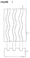
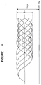
- Figure 1 shows a schematic view illustrating wobbling grooves 2 formed on the surface of a substrate 1.
- the wobbling is called “wobble” and frequency-modulated (FM) by a carrier frequency of 22.05 kHz, and its amplitude (Wobble Amplitude) is very small at a level of 30 nm as compared with the pitch of grooves 2 (i.e. the distance between the imaginary center lines of grooves 2: usually about 1.6 ⁇ 0.1 ⁇ m).
- Such a wobble frequency-modulated by absolute time information or address information is called ATIP (Absolute Time In Pre-groove) or ADIP (Address In Pre-groove), which has already been used in a recordable compact disk (CD-Recordable, CD-R) or in a mini disk ("CD family", coauthored by Heitaro Nakajima, Takao Inohashi and Hiroshi Ogawa, Ohm-sha (1996) chapter 4 and Proceedings of the IEEE, vol. 82 (1994) p. 1490).
- the recording process of the above phase-change medium involves a drastic heat cycle such that the recording layer is melted and then quenched to a temperature lower than the melting point within a few tens nano seconds. Therefore, even if the recording layer is sandwiched by dielectric protective layers, microscopic deformations and segregations will be accumulated by repetitive overwriting for a few thousands to a few tens thousands times, and will eventually lead to an increase of optically recognizable noises or formation of local defects of micron order (J. Appl. Phys., 78 (1995), pp 6980-6988).
- the groove geometry is required to secure the compatibility of groove signals with the CD standards, rather lowers the repetitive overwriting durability of the phase-change medium. Namely, within a range of the groove geometry (depth: 20 to 100 nm, width: 0.2 to 0.8 ⁇ m) where there will be no trouble in tracking servo (a push-pull method or a 3 beam method) with a focused light having a wavelength of 780 nm ⁇ 30 nm, the groove depth is required to be less than 60 nm, and the groove width is required to be within a range of from 0.3 to 0.6 ⁇ m in order to bring push-pull signals after recording to the same level as ROM standards (about 0.04 to 0.09) to secure the compatibility with CD-ROM (JP-A-8-21550, but this patent concerns nothing about the repetitive overwriting durability).
- This relation is a parameter determined substantially solely by the groove geometry, which does not substantially depend on the multilayer structure of the phase-change medium.
- the overwriting durability has to be sacrificed to some extent, but it is desired to minimize such a sacrifice.
- the lower protective layer has a function of not only suppressing the temperature rise of the substrate surface by the heat insulating effect but also mechanically suppressing the deformation of the substrate. Accordingly, a ZnS-SiO 2 mixture film or the like is widely used from the viewpoint of the thermal conductivity and mechanical properties.
- the present inventors have found the following solutions to the above-mentioned problems encountered in the course of developing CD-RW employing a phase-change medium, and the present invention has been accomplished on the basis of such solutions.
- the present invention provides an optical information recording medium comprising a substrate provided with periodically wobbling guide grooves with a track pitch of 1.6 ⁇ 0.1 ⁇ m, and a lower protective layer, a phase-change type recording layer, an upper protective layer and a reflective layer formed in this sequence on the substrate, for recording, retrieving and erasing amorphous marks in the guide grooves by modulation of light intensity of at least two levels by means of a focused light having a wavelength of 780 ⁇ 30 nm applied from the side of the substrate opposite to the recording layer side so that a crystalline state with a reflectance of from 15 to 25% is an unrecorded state, and an amorphous state with a reflectance of less than 10% is a recorded state, wherein the recording layer is a thin film of an alloy of My y (Sb x Te 1-X ) 1-y where 0 ⁇ y ⁇ 0.3, 0.5 ⁇ x ⁇ 0.9, and My is at least one member selected from the group consisting of In, Ga, Zn,
- the present invention provides an optical information recording medium comprising a substrate provided with periodically wobbling guide grooves with a track pitch of 1.6 ⁇ 0.1 ⁇ m, and a first lower protective layer, a second lower protective layer, a phase-change type recording layer, an upper protective layer and a reflective layer formed in this sequence on the substrate, for recording, retrieving and erasing amorphous marks in the guide grooves by modulation of light intensity of at least two levels by means of a focused light having a wavelength of 780 ⁇ 30 nm applied from the side of the substrate opposite to the recording layer side so that a crystalline state with a reflectance of from 15 to 25% is an unrecorded state, and an amorphous state with a reflectance of less than 10% is a recorded state, wherein the recording layer is a thin film of an alloy of My y (Sb x Te 1-x ) 1-y where 0 ⁇ y ⁇ 0.3, 0.5 ⁇ x ⁇ 0.9, and My is at least one member selected from the group consisting of In
- the present invention provides an optical information recoding medium which is a rewritable optical information recording medium comprising a substrate and a phase-change type recording layer comprising Sb x Te 1-x , where 0.6 ⁇ x ⁇ 0.85, as the main component, formed on the substrate, wherein a readily crystallizable crystallization accelerating layer is formed between the substrate and the recording layer in contact with the recording layer in a thickness of from 0.2 to 5 nm, and the recording layer is treated for initial crystallization by irradiation with light energy.
- a rewritable optical information recording medium comprising a substrate and a phase-change type recording layer comprising Sb x Te 1-x , where 0.6 ⁇ x ⁇ 0.85, as the main component, formed on the substrate, wherein a readily crystallizable crystallization accelerating layer is formed between the substrate and the recording layer in contact with the recording layer in a thickness of from 0.2 to 5 nm, and the recording layer is treated for initial crystallization by irradiation with light energy.
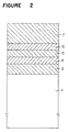
- the optical information recording medium used in the present invention has a structure of substrate 1/dielectric lower protective layer 3/recording layer 4/dielectric upper protective layer 5/reflective layer 6. It is preferred that the top is coated with an ultraviolet-curable or thermosetting resin (protective coating layer 7).
- a transparent resin such as polycarbonate, acrylic resin or polyolefin, or glass
- a polycarbonate resin is most preferred, since it is inexpensive and has been most commonly practically used in CD.
- the recording layer 4, the protective layers 3 and 5 and the reflective layer 6 are formed by e.g. a sputtering method. With a view to preventing oxidation or contamination among the respective layers, it is preferred to carry out the film formation in an in-line apparatus wherein the target for the recording layer, the targets for the protecting layers and, if necessary, the target for the reflective layer, are disposed in the same vacuum chamber.
- the lower protective layer 3 is provided on the surface of the substrate 1, and the upper protective layer 5 is provided on the recording layer 4, usually in a thickness of from 10 to 500 nm.
- such a protective layer made of e.g. a dielectric material is less than 10 nm, the effect for preventing deformation of the substrate l or the recording layer 4 tends to be inadequate, and such a layer tends to be useless as a protective layer. If the thickness exceeds 500 nm, the internal stress of the dielectric material itself or the difference in the elastic property from the substrate 1 tends to be distinctive, whereby cracking is likely to occur.
- the materials for the upper and lower protective layers are determined taking into consideration the refractive indices, the thermal conductivities, the chemical stability, the mechanical strength, the adhesion, etc.
- an oxide, sulfide or nitride of e.g. Mg, Ca, Sr, Y, La, Ce, Ho, Er, Yb, Ti, Zr, Hf, V, Nb, Ta, Zn, Al, Si, Ge or Pb, or a fluoride of Ca, Mg or Li having high transparency and high melting point, can be used.
- oxides, sulfides, nitrides and fluorides may not necessarily take stoichiometrical compositions.
- a dielectric mixture is preferred. More specifically, a mixture of ZnS or a rare earth sulfide with a heat resistant compound such as an oxide, nitride or carbonate, may be mentioned.
- a particularly preferred structure may, for example, be such that the portion of the lower protective layer in a thickness of from 1 to 10 nm on the side which is in contact with the recording layer, is made of a mixture comprising a chalcogen compound and a heat resistant compound having a decomposition temperature or melting point of at least 1,000°C, which is not a chalcogen compound, and the remaining portion is made of a heat resistant compound of the type which is the same or different from the above heat resistant compound.
- the chalcogen compound may, for example, be, in addition to ZnS and ZnSe, a sulfide of a Group IIa element such as MgS, CaS, SrS or BaS, a sulfide of a rare earth, such as La 2 S 3 or Ce 2 S 3 , a selenium compound of a Group IIa element such as MgSe, CaSe, SrSe or BaSe, or a selenium compound of a rare earth such as La 2 Se 3 or Ce 2 Se 3 . Further, a sulfide or a selenium compound of Ta or Nb may also be used.
- a sulfide or a selenium compound of Ta or Nb may also be used.
- the above sulfides or selenium compounds contain chalcogen elements and thus have good adhesion with chalcogen elements mainly contained in the phase-change type recording layer and with the surrounding elements. Thus, a substantial improvement in the repetitive recording characteristic is observed as compared with a case where a dielectric layer made merely of an oxide is employed.
- the heat resistant compound other than the chalcogen compound may, for example, be an oxide of Al, Si, Ge, Y, Zr, Ba, Ta, Nb, V, W, Hf, Sc or a lanthanoid, a nitride of Al, Si, Ge, Ta or B, a fluoride of Mg, Ca, Nd, Tb or La or a carbide of Si or B.
- silicon dioxide yttrium oxide, barium oxide, tantalum oxide, LaF 3 , NdF 3 , TbF 3 , SiC, Si 3 N 4 or AlN.
- the total amount of the above chalcogen compound and the heat resistant compound other than a chalcogen compound in the protective layer is preferably at least 50 mol%, more preferably at least 80 mol%. If their content is less than 50 mol%, the effect for preventing deformation of the substrate or the recording layer tends to be inadequate, and the layer tends to be useless as a protective layer.
- the content of the chalcogen compound is preferably from 10 to 95 mol% of the entire protective layer. If the content is less than 10 mol%, the desired property tends to be hardly obtainable. On the other hand, if it exceeds 95 mol%, the optical absorption coefficient tends to be large, such being undesirable.
- the content is more preferably from 15 to 90 mol%.
- the content of the above heat resistant compound is preferably from 5 to 90 mol% in the entire protective layer, more preferably at least 10 mol%. If the content is outside this range, the desired property may not sometimes be obtained.
- the heat resistant compound is required to have a heat resistance of at least 1,000°C, and at the same time, required to be optically adequately transparent to the laser beam to be used for recording and retrieving. Namely, in a thickness of 50 nm, the imaginary part of the complex refractive index in a wavelength region of at least about 600 nm is desired to be at most 0.1.
- S or Se in a sulfide or a selenium compound has a high vapor pressure, and a part thereof tends to evaporate or undergo decomposition during the sputtering. If such deficiency of S or Se in a protective layer becomes substantial, the optical absorptivity tends to be defective, and the protective layer tends to be chemically unstable. Addition of oxygen or nitrogen to the sputtering gas as mentioned above, is intended to replace such deficiency with oxygen or nitrogen.
- an oxide or nitride of the metal element of the above chalcogen compound will be formed partially in the film, but such an oxide or nitride serves as a part of the heat resistant compound, whereby the properties of the film will not be impaired.
- the film density of these protective layers is preferably at least 80% of the bulk density from the viewpoint of mechanical strength (Thin Solid Films, vol., 278, (1996), p. 74-81).
- the recording layer of the medium of the present invention is a phase-change type recording layer, and its thickness is usually preferably within a range of from 10 to 100 nm. If the thickness of the recording layer is thinner than 10 nm, no adequate contrast tends to be obtained, and the crystallization speed tends to be slow, whereby it tends to be difficult to erase the recorded information in a short time. On the other hand, if it exceeds 100 nm, an optical contrast tends to be hardly obtainable, and cracking is likely to occur, such being undesirable. Further, in order to obtain a contrast sufficient for the compatibility with CD, the thickness of the recording layer is limited within a range of from 15 to 30 nm. If the thickness is less than 15 nm, the reflectance tends to be too low, and if it exceeds 30 nm, the heat capacity tends to be large, whereby the recording sensitivity tends to be poor.
- mark length recording is applied as in the case of CD-RW
- a thin film of an alloy comprising, as the main component, a SbTe alloy close to the Sb 70 Te 30 eutectic point, for the recording layer, from the viewpoint of the after-mentioned optical properties and crystallizability.
- an alloy material close to a eutectic composition has been believed to be unsuitable as a recording layer for a rewritable optical recording medium, since it undergoes phase separation during crystallization although its amorphous forming ability is high, and it can not be crystallized by heating in such a short period of time as less than 100 nano seconds (Appl. Phys. Lett., vol., 49 (1986), p. 502).
- US Patent 5,015,548 discloses that the in the vicinity of the Sb 70 Te 30 eutectic composition, a Sb x Te 1-x (0.58 ⁇ x ⁇ 0.75) binary alloy is useful for repeated recording and erasing between the crystalline and amorphous states, although the method is quite primitive wherein only the change in reflectance is monitored.
- a composition having a third element, particularly Ge, added to Sb 70 Te 30 JP-A-1-115685, JP-A-1-251342, JP-A-1-303643 and JP-A-4-28587 may, for example, be mentioned.
- phase-change media in the vicinity of the SbTe eutectic composition, there has been no practical progress since then. Especially, there has been a serious problem that the initialization operation to crystallize the recording layer after film formation, is difficult, and the productivity is too low for practical application.
- the present inventors have paid a particular attention to a binary alloy composed of SbTe for simplification and have conducted a review of the crystallization/amorphous conversion characteristics in the vicinity of the eutectic composition from the viewpoint of applicability to mark length recording by means of an optical disk evaluating machine more suitable for high density recording, without being influenced by the conventional theories.
- a recording layer comprising, as the main component, a SbTe alloy close to the Sb 70 Te 30 eutectic composition is hardly susceptible to initial crystallization, but once it has been initially crystallized, the subsequent writing and erasing by the phase change between the amorphous and crystalline states can be carried out at an extremely high speed.
- a thin layer of an alloy of the formula My y (Sb x Te 1-x ) 1-y (0 ⁇ y ⁇ 0.3, 0.5 ⁇ x ⁇ 0.9, and My is at least one member selected from the group consisting of In, Ga, Zn, Ge, Sn, Si, Cu, Au, Ag, Pd, Pt, V, Nb, Ta, Pb, Cr, Co, O, S and Se), is used.
- In, Ga, Ge, Sn, Cu, Pb, V, Nb, Ta, O, Se and S are effective to increase the crystallization temperature of the SbTe eutectic alloy and thus to improve the stability with time. Further, they are effective for fine adjustment of the optical constant (complex refractive index).
- Au, Ag, Pd, Pt and Zn are effective to facilitate crystallization (initialization) of an amorphous film in the state immediately after the film formation (as-deposited state).
- the most important merit of employing the material for the recording layer of the present invention is that coarse grains having a reflectance different from the initialized state, scarcely form in the periphery of an amorphous mark or in the erased mark. This is a phenomenon specific to an alloy close to the eutectic point, wherein the crystal growth is controlled by the phase separation.
- this recording layer has a characteristic such that if the crystallization speed in a solid phase is increased, the recrystallization speed during resolidification at the time of forming an amorphous mark also tends to be extremely high, whereby the periphery of the molten region tends to undergo recrystallization, whereby formation of an amorphous mark tends to be inadequate.
- this recording layer has a composition close to the eutectic point
- the crystallization speed is governed by the diffusing speed of atoms for phase separation, whereby high speed erasing by crystallization can not be accomplished unless heating is carried out to a level immediately below the melting point, where the diffusing speed becomes maximum.
- the temperature range within which a high crystallization speed is obtainable is narrow and shifted to a high temperature side.
- the optical information recording medium of the present invention a phenomenon has been utilized such that the recording layer material undergoes phase separation basically into a Sb phase and a Sb 2 Te 3 phase on the line where the Sb 70 Te 30 ratio is constant.
- the recording characteristic of the medium of the present invention i.e. the reversible process of amorphous conversion and crystallization, is primarily determined by the Sb/Te ratio, that is, the excess Sb amount contained in the matrix Sb 70 Te 30 eutectic composition. If Sb increases, sites of Sb clusters which precipitate in the super-cooled state will increase, whereby formation of crystal nuclei will be promoted. This means that even when the same crystal growing rate from the respective crystal nuclei is assumed, the time required until the space is filled with grown crystal particles will be shortened, and consequently, the time required for crystallization of the amorphous mark can be shortened. Accordingly, this is advantageous when erasing is carried out at a high linear velocity by irradiation of a laser beam in a short period of time.
- the cooling rate of the recording layer depends also on the linear velocity during recording. Namely, even with the same multilayer structure, the cooling rate lowers as the linear velocity is low. Accordingly, as the linear velocity is low, it is preferred to employ a composition whereby the critical cooling rate for the formation of an amorphous state is small i.e. a composition in which the excess Sb amount is small.
- Addition of In and Ge is particularly effective to improve the thermal stability of the amorphous state and to improve the archival stability of the amorphous recording bit.
- the crystallization time can be shortened in the after-mentioned initialization operation. Both of them may be used in combination.
- the linear velocity dependency as the entire My-SbTe alloy of the present invention is determined by the excess Sb amount contained in the Sb 70 Te 30 composition as the base.
- the excess Sb amount may be increased as described above. However, if it is increased too much, the stability of the amorphous bit tends to be impaired. Therefore, with respect to the Sb x Te 1-x ratio, 0.60 ⁇ x ⁇ 0.85, preferably 0.65 ⁇ x ⁇ 0.80.
- compositional range of the recording layer of the present invention itself is partly disclosed in e.g. JP-A-4-191089, JP-A-4-232779, JP-A-6-166268, and JP-A-8-22644 (especially in JP-A-8-22644), but it is different from the ranges specifically disclosed in Examples of these publications.
- the linear velocity dependency is determined by Sb and Te as the main components. Also with a AgInSbTe system, if Sb is contained in an amount of at least 65 atomic%, amorphous mark formation at a low linear velocity tends to be difficult, and if it is less than 55 atomic%, the crystallization speed tends to be too slow, and no adequate erasing can be accomplished.
- the optimum composition is chosen taking into consideration the heat distribution determined by the multilayer structure.
- Addition of In is effective to raise the crystallization temperature and thus to improve the archival stability of the amorphous recording bit. To secure the storage stability at room temperature, it is required to be at least 3 atomic%. However, if it is contained more than 8 atomic%, the phase separation is likely to take place, and segregation is likely to result by repetitive overwriting, such being undesirable.
- Ag is used to facilitate initialization of the amorphous film immediately after the film formation. However, if it is added in an amount of not more than 3 atomic%, no adequate effects can be obtained. On the other hand, the addition in an amount of less than 10 atomic% is usually sufficient, although the amount may vary depending upon the method for initialization. If the amount is too much, the archival stability will be impaired.
- an alloy having a composition of Mw w Ge z (Sb x Te 1-x ) 1-z-w , where Mw is at least one member of Ag and Zn, 0.60 ⁇ x ⁇ 0.85, 0.01 ⁇ z ⁇ 0.20, 0.01 ⁇ w ⁇ 0.15, and 0.02 ⁇ z+w ⁇ 0.30 , may be mentioned.
- an intermetallic compound composition such as Ge 1 Sb 4 Te 7 , Ge 1 Sb 2 Te 4 , Ge 2 Sb 2 Te 5 or GeTe, tends to undergo significant phase separation, which in turn tends to cause the compositional change by repetitive overwriting, such being undesirable. More preferably, the amount is at most 15 atomic%. Further, if it is less than 1 atomic%, no substantial effects of the addition will be obtained.
- the amount of Ag and Zn singly or in combination is from 1 to 15 atomic%. If the amount is less than 1 atomic%, no adequate effects of the addition will be obtained, and if it exceeds 15 atomic%, the effects for stabilizing the amorphous bits by the addition of Ge tend to be lost. Further, the jitter of the recorded mark edge deteriorates probably due to precipitation of a new alloy phase, such being undesirable. Preferably, the amount is at most 10 atomic%. If the total amount of Ag or Zn and Ge is 30 atomic% or more, segregation is likely to result during repetitive overwriting, such being undesirable.
- the crystallization is slow, and the productivity is not good. It is believed necessary that the recording layer composition is once subjected to phase separation from the amorphous state immediately after the film formation (as-deposited state) to form a stable crystalline state, and for this phase separation, heating in a solid phase (at a temperature of not higher than melting point) for at least one ⁇ sec., is usually required.
- initial crystallization of a medium using e.g. Ge 10 Sb 66 Te 24 as the recording layer is attempted under such a condition that when Ge 2 Sb 2 Te 5 is employed as a recording layer, the medium in as-deposited state can be crystallized at a sufficiently high speed, substantial portions tend to remain in an amorphous state without being crystallized. If this operation is repeated a few tens times, the phase separation may be completed, and the initialization may thus be accomplished. However, such is not practical, as the productivity is low. However, once initialization has been done, subsequent crystallization (erasing) can be carried out at a high speed.
- subsequent crystallization erasing
- Initialization is most practically carried out usually by irradiation of a laser beam focused to a size of from a few tens to a few hundreds ⁇ m (bulk erase).
- the substrate is made of a plastic, it is not possible to carry out crystallization by raising the temperature of the entire substrate to a level of the crystallization temperature (usually at least 150°C) of the recording layer, because the substrate is likely to be softened and deformed at such a high temperature.
- a level of the crystallization temperature usually at least 150°C
- melt initialization is effective for the recording layer of the present invention. This is effective to remarkably increase the crystal growth rate.
- Ag, Au, Pd, Pt, Zn or the like functions as crystal nuclei.
- the recording medium will not immediately be destroyed even when the recording layer is melted.
- the recording medium will not be destroyed, if melting is limited to the center portion of a beam by local heating by means of a light beam (gas laser beam or a semiconductor laser beam) focused in e.g. an oval shape with a long axis of from 10 to 100 ⁇ m and a short axis of from 1 to 10 ⁇ m.
- a light beam gas laser beam or a semiconductor laser beam
- the melted portion is heated by remaining heat along the periphery of the beam, whereby the cooling rate tends to be slow, and good recrystallization will be carried out.
- the melt initialization itself is a known method.
- the present inventors have found that this method is particularly effective for the recording medium of the present invention. Namely, by this method, the time for initialization can be shortened to one tenth as compared with conventional solid phase crystallization, whereby the productivity is increased to a large extent.
- melt initialization provides an effect of preventing a change in the crystallizability during erasing after overwriting.
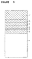
- the present inventors have found it effective to provide a certain specific crystallization accelerating layer 8 on the lower protective layer side 3 in contact with the recording layer 4, as shown in Figure 3, whereby the initial crystallization can be completed in a short period of time.
- the crystallization accelerating layer serves as crystal nuclei to promote the crystallization, or that the structure in the as-deposited state of the recording layer formed on the crystallization accelerating layer is different from the case where no crystallization accelerating layer is present, whereby crystallization readily proceeds.
- the initial crystallization can be facilitated when the crystallization accelerating layer is formed below the recording layer, but the effect tends to be small when the crystallization accelerating layer is formed on the recording layer. This indicates that the effect of the latter reason is predominant.
- the crystallization accelerating layer may be made of a readily crystallizable metal such as Au, Ag, Cu or Al, but is preferably the one having a refractive index which is close to the recording layer. Therefore, for the recording layer of the composition of the present invention, the crystallization accelerating layer is preferably of a composition close to Sb 2 Te 3 .
- composition close to Sb 2 Te 3 is, in many cases, crystalline even in the as-deposited state and likely to form crystal nuclei during the initial crystallization, and it also has a merit that it makes the as-deposited state of the recording layer formed thereon a readily crystallizable state.
- compositional range of the crystallization accelerating layer of Sb x Te 1-x is preferably 0.3 ⁇ x ⁇ 0.5, more preferably 0.35 ⁇ x ⁇ 0.45. Further, an additional element may be incorporated in an amount of at most 10 atomic%. For example, Ge 1 Sb 4 Te 7 or the like is useful for the crystallization accelerating layer.
- the effect of providing the crystallization accelerating layer is particularly effective for a recording layer of Ge y (Sb x Te 1-x ) 1-y , where 0.60 ⁇ x ⁇ 0.85 and 0.01 ⁇ y ⁇ 0.20, which contains no crystallization accelerating additional element.
- the crystallization accelerating layer provided at the time of forming the recording layer is considered to be mixed with other portions of the recording layer.
- the thickness of the crystallization accelerating layer is usually from 0.2 to 5 nm, preferably at least 1 nm.
- the crystallization accelerating layer has a composition which is different from the average composition of the recording layer, and the refractive index is different from the recording layer. Accordingly, if it is too thick, the reflectance after the initial crystallization will be different from a case where no crystallization accelerating layer is present. Likewise, the reflectance will be different as between after the initial crystallization and after repetitive overwriting for e.g. ten times.
- composition-adjusting layer in contact with the crystallization accelerating layer to bring the composition obtained by averaging the compositions of the crystallization accelerating layer and the composition-adjusting layer.
- composition and the multilayer structure of the medium of the present invention represent indispensable improvements to make the alloy close to the Sb 70 Te 30 eutectic composition useful for a practical phase-change medium.
- the present invention is very important also from the viewpoint that the composition which used to be considered difficult to initialize and impractical as a recording layer, has been found to be suitable for high density recording once it has been initialized.
- the reflective layer is provided to positively utilize the optical interference effect to increase the signal amplitude and to let it function as a heat dissipating layer to readily attain a super-cooling state required for forming amorphous marks.
- a metal having a high reflectance and a high thermal conductivity is preferred for the reflective layer.
- Au, Ag or Al may, for example, be mentioned.
- a semiconductor such as Si or Ge may sometimes be used.
- an Al alloy having e.g. Ta, Ti, Cr, Mo, Mg, Zr, V or Nb added to Al in an amount of from 0.5 to 10 atomic%, is preferred. Particularly preferred is Ta or Ti.
- the thermal conductivity can be controlled.
- a characteristic such that the thermal conductivity usually decreases as the amount of impurities in Al is large the thermal conductivity can be controlled.
- a highly corrosion resistant material can be obtained (JP-A-1-16975).
- the thermal conductivity can be controlled within a wide range of from 1/3 to 1/4 of pure Al.
- composition and the thickness of the reflective layer is optimized with a view to controlling the cooling rate of the recording layer via the upper protective layer for forming amorphous marks.
- the thickness is preferably at most 200 nm. However, if it is too thin, the cooling effect tends to be inadequate. Accordingly, the thickness is preferably at least 50 nm.
- the thickness of the upper protective layer is preferably from 10 to 30 nm.
- the thickness of the upper protective layer is rather thick at a level of from 25 to 30 nm, and the reflective layer is made of Al 1-b Ta b (0.01 ⁇ b ⁇ 0.02) having high thermal conductivity in a thickness of from 50 to 150 nm.
- the thicknesses of the recording layer and the protective layers will be described in further detail.
- the thicknesses are selected so that the laser beam absorption efficiency in the recording layer is good and the amplitude of the recorded signals i.e. the contrast between the recorded stated and the unrecorded state, is large.
- the thickness of the upper protective layer is preferably from 10 to 30 nm. The most important reason is that heat dissipation to the reflective layer is most efficiently be carried out.
- a high erasing ratio can be accomplished by high speed crystallization while avoiding problems involved in recrystallization.
- the thickness of the upper protective layer is thicker than 30 nm, the time until the heat of the recording layer reaches the reflective layer, tends to be long, whereby the heat dissipating effect by the reflective layer will hardly be obtainable.
- the reflective layer serves as a pump for pumping out heat
- the upper protective layer serves as a piping to transfer the heat current to the pump.
- the protective layer being thick means the piping being long, whereby even if the performance of the pump is high (even if the thermal conductivity of the reflective layer is high), the performance does not effectively function. Especially when the thickness of the protective layer exceeds 25 nm, it will be required to secure the heat dissipating effect by the reflective layer. For this purpose, it will be necessary to employ a reflective layer having a high thermal conductivity and a thickness of at least 100 nm.
- an Al alloy having an impurity content of less than 2.0 atomic% may be mentioned. Further, Au or Ag is preferred from the viewpoint of the high thermal conductivity.
- the flow rate of a piping may also depend upon the thickness of the piping i.e. upon the thermal conductivity of the upper protective layer.
- the thermal conductivity of a thin film of less than 100 nm is usually smaller by from 2 to 3 figures than the thermal conductivity of the bulk of the same material. Accordingly, the difference due to the material will be small, and the thickness will be an important factor.
- the upper protective layer is thinner than 10 nm, it is likely to break due to e.g. deformation during melting of the recording layer, such being undesirable. This is undesirable also from such a viewpoint that the heat dissipating effect tends to be too large and the power required for recording tends to be unnecessarily large.
- the multilayer structure proposed here is called "rapid cooling structure" for a phase-change medium and is per se known (JP-A-2-56746 and Jpn. J. Appl. Phys., vol. 28 (1989), suppl. 28-3, p 123).
- this rapid cooling structure is used in combination with the following recording method to accurately control the cooling rate during resolidification of the recording layer, whereby it is possible to fully attain the feature of the recording layer material of the present invention suitable for mark length recording.
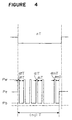
- Figure 4 is a view illustrating one embodiment of the irradiation pattern of a laser power during optical recording in the mark length modulation recording.
- the Figure illustrates an embodiment wherein an amorphous mark having a length nT, where T is a clock period, and n is a natural number of at least 2, is formed so that nT represents a mark length obtainable in the mark length modulation recording.
- bias power Pb of 0 ⁇ Pb ⁇ 0.5Pe is applied, (provided that when 2 ⁇ i ⁇ m-1 , ⁇ i ⁇ i ).
- the laser application period can be adjusted as follows:
- the medium of the present invention it is preferred to carry out recording/erasing by a three power level modulation wherein the above-mentioned off pulse period is provided for bias power Pb, rather than by a two power level modulation with writing power Pw and erasing power Pe as heretofore employed in a conventional GeTe-Sb 2 Te 3 pseudo binary alloy system.
- Overwriting by the two power level modulation may be used, but by employing the three power level modulation system, the power margin and the linear velocity margin for recording can be broadened.
- bias power Pb for the off pulse period it is particularly preferred to adjust bias power Pb for the off pulse period to a sufficiently low level so that 0 ⁇ Pb ⁇ 0.5Pe .
- erasing power Pe is a power which is capable of accomplishing recrystallization of amorphous mark portions with irradiation of less than 100 nano seconds
- writing power Pw is a power which is sufficient for melting the recording layer in a time of ⁇ i T and Pw>Pe.
- Figure 5 is a schematic graph illustrating the temperature change of the recording layer when optical recording is carried out on the medium of the present invention.
- Pb during the off pulse period is substantially 0, whereby the lowest temperature T L ' will be sufficiently lower than the melting point, and the cooling rate is high.
- the amorphous mark is melted during irradiation of the first recording pulse and then is formed by quenching during the subsequent off pulse period.
- the recording layer shows a high crystallization speed only in the vicinity of the melting point.
- the off pulse is suitable, but such off pulse is not necessarily suitable when applied to conventional GeTe-Sb 2 Te 3 type recording layer or when the recording layer of the present invention is applied to the mark position recording as shown in Examples of JP-A-1-303643.
- the modulation is defined by a ratio of I ll /I top , where I top is the top signal level of an EFM signal and I ll is the signal amplitude in the DC retrieving signal (the retrieving signal containing a direct current component) when EFM signal is recorded as shown in Figure 6.
- I top corresponds to the reflectance in the groove of an unrecorded inter-mark portion (crystalline state).
- I ll depends on the intensity difference and the phase difference of reflected lights from the crystalline portion and the amorphous portion of a phase-change medium.
- the intensity difference of the reflected lights is determined basically by the difference in reflectance between the crystalline state and the amorphous state.
- ⁇ negative means that the phase of the amorphous state is progressing, and ⁇ being positive means that the phase of the crystalline state is progressing.
- the land From the beam incident to the substrate surface, the land is located far, and the phase accordingly advances, whereby ⁇ 0. If ⁇ is added to ⁇ , a local interference of a plane wave takes place in the focused laser beam, whereby the reflectance of the amorphous portion recorded in the groove decreases, and a contrast greater than a mere difference in the reflectance between the crystalline state and the amorphous state, may sometimes be obtained.
- the condition for this is: - ⁇ 0
- phase can be irreducible in a cycle of 2 ⁇ . (i.e. eq (4) can be replaced by ⁇ 2 ⁇ )
- Figure 8 illustrates an example of calculation of the reflectance and the phase difference ⁇ between the crystalline and amorphous states in the typical quadri-layer structure.
- Figure 8(a) represents a case of an Ag 5 In 6 Sb 60 Te 29 recording layer as an example of the recording layer material of the present invention
- Figure 8(b) represents a case of Ge 22 Sb 25 Te 43 recording layer which is a prospective phase-change medium material but unsuitable for the present invention.
- the recording layer, the upper protective layer and the refractive layer were 20 nm, 22.5 nm and 200 nm, respectively.
- the change in the amplitude is usually small, and the modulation strongly depends on I top as the denominator i.e. the reflectance in the crystalline state.
- the reflectance in the crystalline state is desired to be as low as possible.
- the thickness of the lower protective layer at which the reflectance in the crystalline state becomes minimum is determined substantially solely by the refractive index of the protective layer in the case of a recording layer having a high reflectance. This is apparent from the fact that in each of Figure 8(a) and 8(b), the minimum points are substantially the same.
- the thickness at the minimum point with other refractive index n can be obtained.
- n is usually from 1.8 to 2.3
- d 1 is only at a level of 85 nm at most. If the refractive index of the lower protective layer is smaller than 1.8, the reflectance at the minimum point increases, whereby the modulation degree substantially decreases to a level of lower than 0.5, such being undesirable.
- the refractive index exceeds 2.3, the reflectance at the minimum point tends to be too low to accomplish 15%, whereby focusing or tracking servo tends to be difficult, such being undesirable.
- phase difference ⁇ it is desired that the phase of the amorphous state progresses, as mentioned above.
- servo tends to be unstable, since the same effect as a change of the groove geometry which takes place simultaneously with recording, will form.
- a push-pull signal tends to be hardly obtainable, such being undesirable.
- the phase difference ⁇ due to the groove depth is only at a level of 0.35 ⁇ at the highest.
- between the crystalline and amorphous states is preferably less than 0.5 ⁇ .
- phase difference ⁇ abruptly changes as the thickness of the lower protective layer changes.
- Ge 22 Sb 25 Te 43 recording layer is not suitable for the recording medium of the present invention utilizing the minimum point in reflectance, although it is close to the Ge 2 Sb 2 Te 5 composition which is prospective as a phase-change medium.
- the deposition rate by sputtering is very slow and less than one third as compared with a metal film. Therefore, the film thickness at the second minimum value in the Figure is not desirable, since it takes a long time for film forming.
- the thickness of the lower protective layer is preferably less than 150 nm. Because, currently, the film forming speed by sputtering for a dielectric protective layer is at a level of 15 nm/sec, and if it takes more than 10 seconds for the film forming, the cost will increase.
- the thickness distribution difference for the practical production is determined by a percentage (%) relative to d 0 , and usually d 0 ⁇ 2 to 3% is the limit for uniformity.
- the smaller d 0 the smaller the variation width ⁇ d in the film thickness, and such is advantageous, since the variation in the reflectance in the disk plane or among disks can be suppressed.
- a film thickness of at least 200 nm may be employed.
- durability of at least 1,000 times is considered to be adequate, and a thickness in the vicinity of d 1 is usually selected from the viewpoint of the cost performance.
- the lower protective layer is required to have a certain thickness.
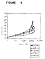
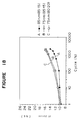
- Figure 9 shows the dependency of the repetitive overwriting durability on the thickness of the lower protective layer.
- the groove width was substantially constant at 0.55 ⁇ m.
- the thickness of the lower protective layer becomes less than 70 nm, the durability abruptly deteriorates. Especially, the jitter abruptly increases at the initial stage where the number of repetitive overwriting is less than a few hundreds times. The deterioration of the jitter during the initial stage of the repetitive overwriting depends largely on the thickness of the lower protective layer.
- the protective layer is required to have a thickness sufficient for a heat insulating effect not to transmit the heat generation of the recording layer and sufficient to mechanically suppress the deformation. It is evident that to attain the durability of at least 1,000 times required for a medium of this type, the thickness is required to be at least 70 nm, preferably at least 80 nm.
- a thickness of at least 70 nm is preferred which is a thickness where the reflectance becomes minimum. More preferably, the thickness is at least 80 nm. Further, in order to minimize the change in reflectance due to a change in the film thickness, the thickness is preferably at most 90 nm.
- phase difference ⁇ adversely affects, whereby an amplitude expected from the difference in reflectance can not be obtained.
- the requirement in this respect is to employ a film thickness thicker by more than 0 nm and not more than 30 nm than d 1 at the first minimum point of reflectance.
- a medium which positively utilizes the above phase difference ⁇ may be mentioned. Optically, this is preferred in that the modulation can be made larger with the same difference in reflectance.
- a lower protective layer thinner by more than 0 nm and not more than 30 nm than the thickness at the minimum point of reflectance.
- Designing of the multilayer structure except the first lower protective layer 3' is made preferentially taking the optical properties into consideration, and the thickness of the second lower protective layer 3'' is adjusted to be thinner by more than 0 nm and not more than 30 nm, preferably from 2 to 30 nm, than the thickness at the minimum point of reflectance.
- the thickness of the lower protective layer is at least 70 nm in the total of the first lower protective layer 3' and the second lower protective layer 3''. This structure is used to increase the mechanical strength and to improve the repetitive overwriting durability.
- n 1 and n sub are exactly the same, or the difference is less than 0.05. However, there is no practical problem so far as the difference is less than 0.1.
- a typical polycarbonate resin substrate has n sub of 1.55. Accordingly, it is advisable to use a dielectric material having n 1 of from 1.5 to 1.6.
- a mixture of SiO 2 , SiC and Y 2 O 3 , or a mixture of ZnS, SiO 2 and MgF 2 or CaF 2 is preferred, since such a mixture itself is excellent in durability.
- the compatibility with CD can substantially be maintained except that the recording signal quality is of a low reflectance.
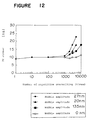
- a groove was formed in a spiral form with a groove pitch of 1.6 ⁇ m, a groove width of about 0.5 ⁇ m and a depth of about 40 nm.
- the groove had a wobble formed in a transverse direction with a frequency of 22.05 kHz.
- the wobble applitudes were four types of 27 nm, 20 nm, 13.5 nm and 0 nm (no wobble).
- the wobble applitudes were measured by a measuring method provided for in the CD-RW standards (Orange Book part 3), but the absolute values themselves are merely values for reference and not critical so long as the relative relations can be controlled.
- Recoding was carried out in the groove to form amorphous marks in the crystalline region.
- the signal quality was evaluated by the severest 3 T jitter.
- the jitter is required to be smaller than 17.5 nsec at the double speed (2.8 m/s).
- the groove wall 10 is susceptible to deterioration by heat damage during repetitive overwriting for such a reason that a stress is likely to collect at the groove wall portion or at the groove corner portion where the adhesion of the thin film is poor, and if a laser beam is applied even slightly to such a groove wall, the deterioration may be accelerated.
- the initial jitter was about 10 nsec in each case.
- the groove width is preferably from 0.4 to 0.6 ⁇ m, more preferably from 0.45 to 0.55 ⁇ m.
- the groove geometry specifically disclosed as preferred in this publication is such that the groove depth is from 50 to 60 nm, and the groove width is from 0.3 to 0.6 ⁇ m.
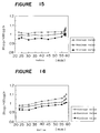
- RC 2(I L -I G )/(I L +I G )
- I L and I G are the intensities of the reflected lights from the land portion and the groove portion, respectively.
- the reflected light intensity is a sum signal I 1 +I 2 of light detectors disposed on both sides of the track center.
- the radial contrast is defined before and after recording.
- the radial contrast after recording is calculated by using the intensity obtained by averaging the signal intensities of the reflection-reduced portions by a low pass filter.
- the push-pull value PPa after recording is defined likewise by using an average value of the difference signal
- as follows: PPa
- this is a push-pull signal output after passing through a low pass filter having a cut off frequency of from 5 to 10 kHz.
- JP-A-8-212550 defines e.g. the groove signal relating to the drive design.
- the thickness of the lower protective layer used in Examples is 200 nm, and the recommended value for the groove depth specifically exemplified is as deep as from 50 to 60 nm.
- the recommended value for the groove depth being large in the above publication is considered to be due to the fact that the lower protective layer is far thick beyond the range of the present invention. Namely, if the lower protective layer is thick, the groove is embedded therewith so that the groove as observed on the recording layer surface will be substantially shallow. Accordingly, it may have been required to set the groove to be rather deep.
- the present invention is substantially different in the overall design concept from the above publication in that not only optical properties, but also the balance of reliability and productivity, is taken into consideration to design the multilayer structure and the groove geometry of the recording medium. Accordingly the effective ranges are different.
- the groove depth is set to be too shallow, production of the stamper or molding of the substrate tends to be difficult, or the radial contrast signal or the push-pull signal tends to be lower than the lower limit of the standards. Therefore, the groove can not be made shallower than 25 nm.
- the groove depth is more preferably from 30 to 40 nm.
- the groove width is preferably at least 0.5 ⁇ m from the viewpoint of the radial contrast and preferably at most 0.6 ⁇ m from the viewpoint of the overwriting durability related to the wobble and the groove geometry.
- the width is wider than 0.6 ⁇ m, deterioration of the overwriting durability tends to be remarkable as a general phenomenon of a phase-change medium.
- the groove width is narrower than 0.4 ⁇ m, deterioration of the overwriting durability due to the presence of a wobble tends to be remarkable, such being undesirable.
- the groove width is from 0.45 to 0.55 ⁇ m.
- the present invention is based on a discovery of a specific means to overcome various restrictions resulting from an attempt to produce a rewritable medium compatible with CD although the reflectance is low and to take a balance among trade off factors beyond a mere optimization procedure.
- Tables 1 and 2 are the repetitive overwriting durability, the optical properties and the groove signal properties when the groove width and the groove depth were changed while maintaining the wobble amplitude to be constant.
- Table 1 shows Examples within the scope of the present invention, and Table 2 shows Comparative Examples outside the scope of the present invention.
- the multilayer structure employed in the experiments was such that the lower protective layer of (ZnS) 80 (SiO 2 ) 20 was 80 nm, the recording layer of Ag 5 In 5 Sb 60 Te 30 was 20 nm, the upper protective layer of (ZnS) 80 (SiO 2 ) 20 was 23 nm, and the reflective layer of Al 98 Ta 2 was 100 nm.
- the film density of the protective layers of (ZnS) 80 (SiO 2 ) 20 was 3.5 g/cm 3 , which was 94% of the theoretical bulk density of 3.72 g/cm 3 . All of the thin films in the multilayer structure were prepared by sputtering without breaking a vacuumed condition.
- the substrate was prepared by injection molding.
- compositions of the layers were confirmed by a combination of fluorescent X-ray analysis, atomic absorption analysis and X-ray excitation photoelectron spectrometry.
- the recording layer in the as-deposited state was amorphous, and the entire area was crystallized to an initial (unrecorded) state by irradiating the disk surface with an elliptic laser diode beam having a long axis of 70 ⁇ m and a short axis of about 2 ⁇ m with an initialization power of 500 mW at a linear velocity of 3 m/s by a bulk eraser (POP 120, tradename, manufacture by Hitachi Computer Kiki).
- POP 120 tradename, manufacture by Hitachi Computer Kiki
- the recording layer is considered to have once melted and crystallized during resolidification.
- Writing power Pw, erasing power Pe and bias power Pb were 12 mW, 6mW and 0.8 mW, respectively. Retrieving power was usually the same as the bias power.
- Measurement of push-pull signal after recording PPa was carried out with respect to the signal passed through a low pass filter with a cut off frequency of 5 kHz.
- the number of times for overwriting durability is the number of times within which a jitter of 3 T mark is maintained at a level of not higher than 17.5 nsec which is the upper limit stipulated by the CD standards, when repetitive overwriting is carried out at the double speed.
- the radial contrast values RCb and RCa after recording are also indicated. If the groove depth exceeds 45 nm, RCa tends to exceed 0.6 such being undesirable.
- the groove depth exceeds 50 nm, the push-pull PPa after recording tends to exceed 0.1, such being undesirable.
- the reflectance in the groove decreased to a level of 15% or lower, whereby the tracking servo was unstable.
- the groove width should be within a range of from 0.4 to 0.6 ⁇ m. Otherwise, repetitive overwriting for 1,000 times can not be accomplished.
- the groove depth is less than 25 nm, the radial contrast ratio between before and after recording becomes substantially lower than 0.3, and the number of times of overwriting will be less than from 500 to 600 times, such being undesirable.
- Example 2 disks were prepared so that the respective lower protective layers have different thicknesses of 80 nm (Example 2) and 260 nm (Comparative Example 2) which are in the vicinity of the minimum points (75 nm and 250 nm) of reflectance. Each disk was prepared in the same sputtering apparatus.
- the film density of each protective layer was about 93% of the bulk density.
- the thickness of the recording layer of Ag 5 In 6 Sb 59 Te 30 was 20 nm
- the thickness of the upper protective layer was 23 nm
- the thickness of the reflective layer was 100 nm.
- Figures 15 and 16 show the distribution in a radial direction of the reflectance of the disks of Example 2 and Comparative Example 2, respectively.
- center bent line shows average values at the respective radii
- upper and lower bent lines show the maximum and minimum values at the respective radii.
- Example 2 Including the distribution in circumferential direction, in Comparative Example 2, the variation was within a range of the average value + 11% and the average value - 7%. On the other hand, in Example 2, the variation was within the average value ⁇ 6%.
- the distribution of reflectance in the same disk plane is desired to be within a range of ⁇ 10 to 12% for an optical disk. From this viewpoint and from the fact that the film deposition time and the cost for materials can be reduced to about 1/3, it is evidently preferred also from the viewpoint of the productivity to employ the thickness of the lower protective layer in the vicinity of the first minimum point of reflectance.
- composition of a lower protective layer of ZnS:SiO 2 and the dependency on the film thickness were studied by using a substrate of Example 1 (b) and a multilayer structure being such that a recording layer of Ag 5 In 5 Sb 59 Te 31 was 20 nm, an upper protective layer of (ZnS) 80 (SiO 2 ) 20 was 23 nm and a reflective layer of Al 98 Ta 2 was 100 nm.
- the groove depth was 35 nm, and the groove width was 0.53 ⁇ m.
- the modulation were 0.699, 0.737, 0.703, 0.656 and 0.631 at points A, B, C, D and E in the Figure, respectively.
- Figure 18 shows the results of evaluation in which repetitive overwriting durability with the lower protective layer shown at A, B or C in Figure 17 was evaluated in the same manner as in Figure 11.
- the same composition may be used for the upper and lower protective layers, or a some compositional difference (difference in the refractive index) may be made, for example by setting 0.13 ⁇ a ⁇ 0.17 for the lower protective layer and 0.18 ⁇ a ⁇ 0.22 for the upper protective layer. Such a choice is suitably determined depending upon the optical requirements.
- Example 1 (b) By using the substrate and the multilayer structure of Example 1 (b), a disk was prepared in the same manner except that the recording layer was changed to an alloy layer of Zn 3 Ge 8 Sb 61 Te 28 .
- the disk was initialized by a bulk eraser and then subjected to overwriting at the double speed of CD in accordance with the recording pulse strategy shown in Figure 11.
- Example 1 (b) On the substrate of Example 1 (b), 80 nm of a (ZnS) 80 (SiO 2 ) 20 layer, 20 nm of an Ag 6 Ge 5 Sb 70 Te 19 layer as a recording layer, 20 nm of a (ZnS) 80 (SiO 2 ) 20 layer and 200 nm of an Al 97.5 Ta 2.5 alloy layer were sequentially deposited by magnetron sputtering, and 4 ⁇ m of an ultraviolet-curable resin layer was further formed thereon to obtain an optical disk.
- a (ZnS) 80 (SiO 2 ) 20 layer On the substrate of Example 1 (b), 80 nm of a (ZnS) 80 (SiO 2 ) 20 layer, 20 nm of an Ag 6 Ge 5 Sb 70 Te 19 layer as a recording layer, 20 nm of a (ZnS) 80 (SiO 2 ) 20 layer and 200 nm of an Al 97.5 Ta 2.5 alloy layer were sequentially deposited by magnetron s
- This optical disk was subjected to melt initial crystallization by means of another optical disk initializing apparatus using an elliptic beam with a wavelength of 810 nm and with a long axis of 50 ⁇ m and a short axis of about 2 ⁇ m, at a linear velocity of 4.5 m/s, a beam radial transferring speed of 5 ⁇ m/rotation with a laser power of 250 mW, whereby initial crystallization was possible.
- the jitter value showing the actual signal characteristic was less than 10% of the clock period for the shortest mark length, and thus a good characteristic was obtained. Further, this characteristic was maintained even after repetitive overwriting for 1,000 times.
- the recorded signal was left to stand for 1,000 hours in an environment at a temperature of 80°C under a relative humidity of 80%, whereby no deterioration was observed in the recorded signal.
- Example 1 (b) On the substrate of Example 1 (b), 80 nm of a (ZnS) 80 (SiO 2 ) 20 layer, 20 nm of a Ge 7 Sb 60 Te 27 Zn 6 layer as a recording layer, 20 nm of a (ZnS) 80 (SiO 2 ) 20 layer and 200 nm of an Al 97.5 Ta 2.5 alloy layer, were sequentially deposited by magnetron sputtering, and 4 ⁇ m of an ultraviolet-curable resin layer was further formed thereon to obtain an optical disk.
- a (ZnS) 80 (SiO 2 ) 20 layer On the substrate of Example 1 (b), 80 nm of a (ZnS) 80 (SiO 2 ) 20 layer, 20 nm of a Ge 7 Sb 60 Te 27 Zn 6 layer as a recording layer, 20 nm of a (ZnS) 80 (SiO 2 ) 20 layer and 200 nm of an Al 97.5 Ta 2.5 alloy layer, were sequentially deposited
- This optical disk was subjected to melt initial crystallization by means of another optical disk initializing apparatus using an elliptic beam with a wavelength of 810 nm and with a long axis of 50 ⁇ m and a short axis of about 2 ⁇ m, at a linear velocity of 4.5 m/s, a beam radial transferring speed of 5 ⁇ m/rotation with a laser power of 250 mW, whereby initial crystallization was possible.
- the jitter value showing the actual signal characteristic was less than 10% of the clock period for the shortest mark length, and thus a good characteristic was obtained. Further, this characteristic was maintained even after repetitive overwriting for 1,000 times.
- the recorded signal was left to stand for 1,000 hours in an environment at a temperature of 80°C under a relative humidity of 80%, whereby no deterioration was observed in the recorded signal.
- Example 1 (b) On the substrate of Example 1 (b), 80 nm of a (ZnS) 80 (SiO 2 ) 20 layer, 1 nm of a Sb 2 Te 3 layer as a crystallization accelerating layer, 1 nm of a Sb layer as a composition-adjusting layer, 18 nm of a Ge 10 Sb 67 Te 23 layer as a recording layer, 20 nm of a (ZnS) 80 (SiO 2 ) 20 layer and 100 nm of an Al 97.5 Ta 2.5 alloy layer, were sequentially deposited by magnetron sputtering, and 4 ⁇ m of an ultraviolet-curable resin layer was further formed thereon to obtain an optical disk.
- a (ZnS) 80 (SiO 2 ) 20 layer On the substrate of Example 1 (b), 80 nm of a (ZnS) 80 (SiO 2 ) 20 layer, 1 nm of a Sb 2 Te 3 layer as a crystallization accelerating layer, 1 nm
- This disk was subjected to melt initial crystallization by means of another optical disk initializing apparatus using an elliptic beam with a wavelength of 810 nm and with a long axis of 50 ⁇ m, at a disk rotational speed of 2,700 rpm at a beam radial transferring speed of 5 ⁇ m/rotation, with a laser power of 400 mW, with a radius of 64 mm and a laser power of 170 mW with a radius of 27 mm, whereby initial crystallization was possible.
- the jitter value showing the actual signal characteristic was less than 10% of the clock period for the shortest mark length, and thus a good characteristic was obtained. This characteristic was maintained even after repetitive overwriting for 1,000 times.
- the recorded signal was left to stand for 2,000 hours in an environment at a temperature of 80°C under a relative humidity of 80%, whereby no deterioration was observed in the recorded signal.
- Example 1 (b) On the substrate of Example 1 (b), a first lower protective layer, a second lower protective layer, a recording layer, an upper protective layer and a reflective layer were formed to obtain a recording medium having a 5-layer structure.
- the thicknesses of the respective layers were such that the first lower protective layer was 25 nm, the second lower protective layer was 65 nm, the recording layer was 20 nm, the upper protective layer was 22.5 nm, and the reflective layer was 200 nm.
- the film density was 3.4 g/cc, which was substantially 100% of the theoretical density.
- the refractive index n of this film was 1.50.
- (ZnS) 80 (SiO 2 ) 20 was used, and film forming was carried out by a high frequency (13.56 MHz) sputtering.
- the film density was 3.5 g/cm 3 , which was 94% of the theoretical density.
- the refractive index of this film was 2.07.
- the composition of the recording layer was Ag 5 In 6 Sb 59 Te 30 , and for the reflective layer, an Al 98 Ta 2 alloy was used.
- the recording layer and the reflective layer were formed by direct current sputtering under an Ar gas pressure of 0.7 Pa. Further, an ultraviolet curable resin having a thickness of about 5 ⁇ m was formed thereon.
- the first lower protective layer was optically the same as the substrate and thus negligible.
- the thickness of the second lower protective layer is slightly thinner than the thickness at the minimum value of reflectance, and the phase difference ⁇ was advantageous for groove recording.
- the modulation was at least 0.75 with Pw of at least 11 mW.
- Example 1 (b) On the substrate of Example 1 (b), a lower protective layer, a recording layer, an upper protective layer and a reflective layer were formed to obtain recording medium having a quadri-layer structure.
- the thicknesses of the respective layers were such that the lower dielectric layer was 65 nm, the recording layer was 20 nm, the upper dielectric layer was 22.5 nm, and the reflective layer was 200 nm.
- (ZnS) 80 (SiO 2 ) 20 was formed into a film by high frequency (13.56 MHz) sputtering.
- the composition of the recording layer was Ag 5 In 6 Sb 59 Te 30 , and for the reflective layer, an Al 98 Ta 2 alloy was used.
- the recording layer and the reflective layer were deposited by direct sputtering under an Ar gas pressure of 0.7 Pa. Further, an ultraviolet curable resin having a thickness of about 5 ⁇ m was formed thereon.
- a phase-change medium which provides groove signals compatible with the CD format although the reflectance is low, and which provides a high contrast and undergoes little deterioration by rewriting of data in many times.
Landscapes
- Physics & Mathematics (AREA)
- Optics & Photonics (AREA)
- Chemical & Material Sciences (AREA)
- Inorganic Chemistry (AREA)
- Thermal Transfer Or Thermal Recording In General (AREA)
- Optical Record Carriers And Manufacture Thereof (AREA)
Applications Claiming Priority (3)
| Application Number | Priority Date | Filing Date | Title |
|---|---|---|---|
| JP32520796 | 1996-12-05 | ||
| JP32520796A JP3255051B2 (ja) | 1996-12-05 | 1996-12-05 | 光学的情報記録用媒体 |
| JP325207/96 | 1996-12-05 |
Publications (2)
| Publication Number | Publication Date |
|---|---|
| EP0847049A2 true EP0847049A2 (fr) | 1998-06-10 |
| EP0847049A3 EP0847049A3 (fr) | 2001-08-08 |
Family
ID=18174229
Family Applications (1)
| Application Number | Title | Priority Date | Filing Date |
|---|---|---|---|
| EP97109498A Withdrawn EP0847049A3 (fr) | 1996-12-05 | 1997-06-11 | Support d'enregistrement d'information optique |
Country Status (3)
| Country | Link |
|---|---|
| US (2) | US6115352A (fr) |
| EP (1) | EP0847049A3 (fr) |
| JP (1) | JP3255051B2 (fr) |
Cited By (16)
| Publication number | Priority date | Publication date | Assignee | Title |
|---|---|---|---|---|
| EP0883116A3 (fr) * | 1997-06-03 | 1999-02-10 | Nec Corporation | Support d'enregistrement optique |
| EP0945860A3 (fr) * | 1998-03-26 | 2000-01-19 | Matsushita Electric Industrial Co., Ltd. | Support optique d'enregistrement d'information et procédé d'enregistrement et de reproduction d'information optique |
| WO2000014735A1 (fr) | 1998-09-09 | 2000-03-16 | Mitsubishi Chemical Corporation | Support et procede d'enregistrement optique |
| EP1028421A3 (fr) * | 1999-02-12 | 2000-11-29 | Sony Corporation | Disque optique multi-couche |
| EP1065663A3 (fr) * | 1999-06-30 | 2002-02-06 | Sony Corporation | Support d'enregistrement optique |
| EP1143432A3 (fr) * | 1997-03-27 | 2002-04-24 | Mitsubishi Chemical Corporation | Support d'enregistrement optique |
| EP1182649A4 (fr) * | 1999-05-19 | 2003-01-22 | Mitsubishi Chem Corp | Procede d'enregistrement optique et support d'enregistrement optique |
| US6511788B1 (en) * | 1999-02-12 | 2003-01-28 | Sony Corporation | Multi-layered optical disc |
| EP1143431A3 (fr) * | 2000-03-27 | 2003-03-12 | Sony Corporation | Support d'enregistrement optique |
| EP1286345A3 (fr) * | 2001-07-02 | 2005-08-31 | Ricoh Company, Ltd. | Support d'enregistrement d'informations optiques |
| SG118130A1 (en) * | 2001-05-02 | 2006-01-27 | Samsung Electronics Co Ltd | Optical disc having uniform structure |
| EP1143430A3 (fr) * | 2000-03-31 | 2006-04-19 | Sony Corporation | Support d'enregistrement optique |
| EP1150288A3 (fr) * | 2000-03-31 | 2006-04-19 | Sony Corporation | Support d'enregistrement optique |
| EP1223577A3 (fr) * | 2001-01-10 | 2006-05-24 | Ricoh Company, Ltd. | Support d'enregistrement optique à base de changement de phase |
| EP1486965A3 (fr) * | 2003-06-13 | 2006-07-26 | Matsushita Electric Industrial Co., Ltd. | Support d' enregistrement optique et procédé pour sa fabrication |
| CN101055740B (zh) * | 1998-09-09 | 2010-10-13 | 三菱化学媒体株式会社 | 光学信息记录媒体 |
Families Citing this family (42)
| Publication number | Priority date | Publication date | Assignee | Title |
|---|---|---|---|---|
| US6143468A (en) | 1996-10-04 | 2000-11-07 | Mitsubishi Chemical Corporation | Optical information recording medium and optical recording method |
| ES2201474T3 (es) * | 1997-04-16 | 2004-03-16 | Asahi Kasei Kabushiki Kaisha | Procedimiento para la produccion de un medio de registro de informacion optica y medio de registro de informacion optica producido por el proceso. |
| US20030075778A1 (en) * | 1997-10-01 | 2003-04-24 | Patrick Klersy | Programmable resistance memory element and method for making same |
| JPH11259912A (ja) * | 1997-12-25 | 1999-09-24 | Tdk Corp | 光記録媒体 |
| US6426936B1 (en) | 1998-01-27 | 2002-07-30 | Ricoh Company, Ltd. | Phase-change medium usable in phase-difference tracking |
| JP2000057579A (ja) * | 1998-08-10 | 2000-02-25 | Sony Corp | 光ディスク、光ディスクの記録方法及び光ディスクの原盤の製造装置 |
| EP1128365B1 (fr) * | 1998-10-26 | 2006-06-14 | Mitsubishi Kagaku Media Co., Ltd. | Procede d'enregistrement / reproduction a plusieurs valeurs et support d'enregistrement a plusieurs valeurs et variation de phase |
| US6537721B2 (en) * | 1999-02-15 | 2003-03-25 | Tdk Corporation | Optical recording medium and method for its initialization |
| DE60034974T2 (de) * | 1999-03-15 | 2008-01-24 | Matsushita Electric Industrial Co., Ltd., Kadoma | Optisches Phasenübergangsaufzeichnungsmedium und Herstellungsverfahren |
| TW484126B (en) * | 1999-03-26 | 2002-04-21 | Matsushita Electric Industrial Co Ltd | Manufacturing and recording regeneration method for information record medium |
| JP2000322740A (ja) * | 1999-05-12 | 2000-11-24 | Ricoh Co Ltd | 光記録媒体及びその記録方法 |
| DE60027815T2 (de) | 1999-05-19 | 2006-12-21 | Mitsubishi Kagaku Media Corp., Ltd. | Wiederbeschreibbares optisches Aufzeichnungsmedium und optisches Aufzeichnungsverfahren |
| JP2000357343A (ja) * | 1999-06-11 | 2000-12-26 | Sony Corp | 光記録媒体及び光記録媒体製造用原盤 |
| CN1185642C (zh) * | 1999-08-18 | 2005-01-19 | 皇家菲利浦电子有限公司 | 可重写的光信息记录介质 |
| US6479121B1 (en) * | 1999-09-21 | 2002-11-12 | Ricoh Company, Ltd. | Optical recording medium and method of fabricating same |
| US6432502B1 (en) * | 1999-11-17 | 2002-08-13 | Matsushita Electric Industrial Co., Ltd. | Optical recording medium and method of manufacturing the same |
| US6365256B1 (en) * | 2000-02-29 | 2002-04-02 | Eastman Kodak Company | Erasable phase change optical recording elements |
| JP4112153B2 (ja) * | 2000-03-31 | 2008-07-02 | 株式会社リコー | 光記録媒体の検査方法 |
| CA2377619A1 (fr) * | 2000-04-20 | 2001-11-01 | Koninklijke Philips Electronics N.V. | Support d'enregistrement optique et utilisation d'un tel support d'enregistrement optique |
| CN1201309C (zh) | 2000-06-16 | 2005-05-11 | 三菱化学株式会社 | 光信息记录介质 |
| TWI246075B (en) | 2000-08-02 | 2005-12-21 | Mitsubishi Chem Corp | Optical recording medium and process for producing an optical recording medium |
| TWI226776B (en) * | 2000-12-18 | 2005-01-11 | Koninkl Philips Electronics Nv | Secure super distribution of user data |
| US7803471B1 (en) * | 2000-12-28 | 2010-09-28 | Hitachi Maxell, Ltd. | Magnetic tape, its cleaning method, and optical servotrack forming/cleaning apparatus |
| JP3681725B2 (ja) * | 2000-12-28 | 2005-08-10 | 日立マクセル株式会社 | 磁気テープ |
| US20020160306A1 (en) * | 2001-01-31 | 2002-10-31 | Katsunari Hanaoka | Optical information recording medium and method |
| JP4147753B2 (ja) | 2001-07-02 | 2008-09-10 | ソニー株式会社 | 光情報記録媒体、光情報記録媒体用原盤およびその製造方法 |
| CN1287362C (zh) | 2002-02-13 | 2006-11-29 | 三菱化学媒体株式会社 | 可改写光记录媒体和光记录方法 |
| US6899938B2 (en) | 2002-02-22 | 2005-05-31 | Energy Conversion Devices, Inc. | Phase change data storage device for multi-level recording |
| DE60309232T2 (de) * | 2002-03-05 | 2007-09-06 | Mitsubishi Kagaku Media Co. Ltd. | Phasenwechselaufzeichnungsmaterial für ein Informationsaufzeichnungsmedium und ein Informationsaufzeichnungsmedium dieses verwendend |
| KR100906056B1 (ko) * | 2002-03-19 | 2009-07-03 | 파나소닉 주식회사 | 정보 기록매체와 그 제조 방법 |
| AU2003244963A1 (en) * | 2002-07-04 | 2004-01-23 | Koninklijke Philips Electronics N.V. | Rewritalbe optical data storage medium and use of such a medium |
| WO2004023468A1 (fr) | 2002-09-06 | 2004-03-18 | Mitsubishi Chemical Corporation | Support d'enregistrement d'informations optiques |
| WO2004085168A1 (fr) * | 2003-03-24 | 2004-10-07 | Mitsubishi Chemical Corporation | Materiau d'enregistrement a variation de phase et support d'enregistrement d'informations |
| CN1756668B (zh) * | 2003-04-30 | 2010-05-05 | 三菱化学媒体股份有限公司 | 相变记录材料和信息记录介质 |
| JP2005044491A (ja) * | 2003-07-10 | 2005-02-17 | Ricoh Co Ltd | 光記録媒体およびその製造方法 |
| KR101049985B1 (ko) * | 2003-08-07 | 2011-07-19 | 파나소닉 주식회사 | 광학적 정보 기록 매체와 그 제조 방법, 제조 장치, 기록재생 방법 및 기록 재생 장치 |
| JP2005190642A (ja) * | 2003-12-03 | 2005-07-14 | Ricoh Co Ltd | 光記録媒体 |
| JP2006027034A (ja) * | 2004-07-15 | 2006-02-02 | Tdk Corp | 光記録媒体 |
| JP4793313B2 (ja) | 2007-04-16 | 2011-10-12 | ソニー株式会社 | 光情報記録媒体ならびにその記録および/または再生方法 |
| JP5318107B2 (ja) * | 2008-09-04 | 2013-10-16 | 株式会社東芝 | 情報記録再生装置 |
| AU2009292148A1 (en) * | 2008-09-12 | 2010-03-18 | Brigham Young University | Data storage media containing carbon and metal layers |
| CN106229408A (zh) * | 2016-09-27 | 2016-12-14 | 宁波大学 | 一种高速的伪纳米复合Mg‑Sb‑Te可逆相变薄膜及其制备方法 |
Citations (1)
| Publication number | Priority date | Publication date | Assignee | Title |
|---|---|---|---|---|
| EP0630007A1 (fr) * | 1993-06-17 | 1994-12-21 | Nec Corporation | Milieu d'enregistrement optique d'information |
Family Cites Families (21)
| Publication number | Priority date | Publication date | Assignee | Title |
|---|---|---|---|---|
| US5249175A (en) * | 1988-09-09 | 1993-09-28 | Matsushita Electric Industrial Co., Ltd. | Optical information recording medium and information recording and reproducing method therefor |
| US5156693A (en) * | 1990-02-19 | 1992-10-20 | Ricoh Company, Ltd. | Information recording medium |
| KR950003182B1 (ko) * | 1990-03-14 | 1995-04-01 | 마쯔시다덴기산교 가부시기 가이사 | 광디스크 및 광학정보의 기록방법 |
| US5274623A (en) * | 1990-07-19 | 1993-12-28 | Fuji Photo Film Co., Ltd. | Information recording medium having high modulation degree |
| JP3207230B2 (ja) * | 1992-01-08 | 2001-09-10 | 株式会社リコー | 相変化型情報記録媒体 |
| EP0564260B1 (fr) * | 1992-03-30 | 2000-09-06 | Kabushiki Kaisha Toshiba | Milieu d'enregistrement optique et appareil d'enregistrement/reproduction optique |
| DE69322443T2 (de) * | 1992-06-17 | 1999-08-05 | Matsushita Electric Industrial Co., Ltd., Kadoma, Osaka | Optisches Informationsaufzeichnungsmedium |
| US5882493A (en) * | 1993-12-13 | 1999-03-16 | Ricoh Company, Ltd. | Heat treated and sintered sputtering target |
| KR960700503A (ko) * | 1994-03-25 | 1996-01-20 | 마에다 카쯔노수케 | 광기록매체(Optical Recording Medium) |
| JP3284744B2 (ja) * | 1994-04-20 | 2002-05-20 | 松下電器産業株式会社 | 光学的情報記録媒体 |
| JPH10502202A (ja) * | 1994-06-23 | 1998-02-24 | フィリップス エレクトロニクス ネムローゼ フェンノートシャップ | 光学的情報担体 |
| US5581539A (en) * | 1994-08-12 | 1996-12-03 | Mitsubishi Chemical Corporation | Optical recording medium |
| US5641606A (en) * | 1994-10-05 | 1997-06-24 | Asahi Kasei Kogyo Kabushiki Kaisha | Phase-change optical disks and processes for preparing the same |
| US5785828A (en) * | 1994-12-13 | 1998-07-28 | Ricoh Company, Ltd. | Sputtering target for producing optical recording medium |
| EP1189212A3 (fr) * | 1995-03-28 | 2003-09-17 | Toray Industries, Inc. | Supports d'enregistrement optique et procédé d'enregistrement pour les supports d'enregistrement optique |
| DE19612823C2 (de) * | 1995-03-31 | 2001-03-01 | Mitsubishi Chem Corp | Optisches Aufzeichnungsverfahren |
| US5736657A (en) * | 1995-03-31 | 1998-04-07 | Ricoh Company, Ltd. | Sputtering target |
| DE69731411T2 (de) * | 1996-06-14 | 2006-03-02 | Mitsubishi Chemical Corp. | Optische Phasenänderungsscheibe |
| US6022605A (en) * | 1997-02-28 | 2000-02-08 | Kao Corporation | Optical recording medium and recording/erasing method therefor |
| EP1146509B1 (fr) * | 1997-03-27 | 2005-03-16 | Mitsubishi Chemical Corporation | Support d'enregistrement optique |
| JP3761287B2 (ja) * | 1997-05-29 | 2006-03-29 | Tdk株式会社 | 光記録媒体およびその製造方法 |
-
1996
- 1996-12-05 JP JP32520796A patent/JP3255051B2/ja not_active Expired - Fee Related
-
1997
- 1997-06-11 US US08/873,086 patent/US6115352A/en not_active Expired - Lifetime
- 1997-06-11 EP EP97109498A patent/EP0847049A3/fr not_active Withdrawn
-
1999
- 1999-07-14 US US09/353,288 patent/US6108295A/en not_active Expired - Lifetime
Patent Citations (1)
| Publication number | Priority date | Publication date | Assignee | Title |
|---|---|---|---|---|
| EP0630007A1 (fr) * | 1993-06-17 | 1994-12-21 | Nec Corporation | Milieu d'enregistrement optique d'information |
Cited By (29)
| Publication number | Priority date | Publication date | Assignee | Title |
|---|---|---|---|---|
| EP1143432A3 (fr) * | 1997-03-27 | 2002-04-24 | Mitsubishi Chemical Corporation | Support d'enregistrement optique |
| EP1146509A3 (fr) * | 1997-03-27 | 2002-05-02 | Mitsubishi Chemical Corporation | Support d'enregistrement optique |
| US6117511A (en) * | 1997-06-03 | 2000-09-12 | Nec Corporation | Optical recording media |
| EP0883116A3 (fr) * | 1997-06-03 | 1999-02-10 | Nec Corporation | Support d'enregistrement optique |
| EP0945860A3 (fr) * | 1998-03-26 | 2000-01-19 | Matsushita Electric Industrial Co., Ltd. | Support optique d'enregistrement d'information et procédé d'enregistrement et de reproduction d'information optique |
| US6477135B1 (en) | 1998-03-26 | 2002-11-05 | Matsushita Electric Industrial Co., Ltd. | Optical information recording medium and method for recording and reproduction information thereon |
| CN101055740B (zh) * | 1998-09-09 | 2010-10-13 | 三菱化学媒体株式会社 | 光学信息记录媒体 |
| WO2000014735A1 (fr) | 1998-09-09 | 2000-03-16 | Mitsubishi Chemical Corporation | Support et procede d'enregistrement optique |
| US7539110B2 (en) | 1998-09-09 | 2009-05-26 | Mitsubishi Kagaku Media Co., Ltd. | Optical information recording medium and optical recording method |
| US6996052B1 (en) | 1998-09-09 | 2006-02-07 | Mitsubishi Chemical Corporation | Optical information recording medium and optical recording method |
| EP1047056A4 (fr) * | 1998-09-09 | 2007-07-18 | Mitsubishi Kagaku Media Co Ltd | Support et procede d'enregistrement optique |
| EP1028421A3 (fr) * | 1999-02-12 | 2000-11-29 | Sony Corporation | Disque optique multi-couche |
| US6511788B1 (en) * | 1999-02-12 | 2003-01-28 | Sony Corporation | Multi-layered optical disc |
| USRE42786E1 (en) | 1999-05-19 | 2011-10-04 | Mitsubishi Kagaku Media Co., Ltd. | Optical recording method and optical recording medium |
| USRE45001E1 (en) | 1999-05-19 | 2014-07-08 | Mitsubishi Kagaku Media Co., Ltd. | Optical recording method and optical recording medium |
| US7050377B1 (en) | 1999-05-19 | 2006-05-23 | Mitsubishi Chemical Corporation | Optical recording method and optical recording medium |
| EP1376563A3 (fr) * | 1999-05-19 | 2004-07-14 | Mitsubishi Chemical Corporation | Milieu d'enregistrement optique et méthode d'enregistrement |
| US7085215B2 (en) | 1999-05-19 | 2006-08-01 | Mitsubishi Kagaku Media Co., Ltd. | Optical recording method and optical recording medium |
| EP1182649A4 (fr) * | 1999-05-19 | 2003-01-22 | Mitsubishi Chem Corp | Procede d'enregistrement optique et support d'enregistrement optique |
| EP1065663A3 (fr) * | 1999-06-30 | 2002-02-06 | Sony Corporation | Support d'enregistrement optique |
| US6572947B2 (en) | 2000-03-27 | 2003-06-03 | Sony Corporation | Optical recording medium |
| EP1143431A3 (fr) * | 2000-03-27 | 2003-03-12 | Sony Corporation | Support d'enregistrement optique |
| EP1150288A3 (fr) * | 2000-03-31 | 2006-04-19 | Sony Corporation | Support d'enregistrement optique |
| EP1143430A3 (fr) * | 2000-03-31 | 2006-04-19 | Sony Corporation | Support d'enregistrement optique |
| EP1223577A3 (fr) * | 2001-01-10 | 2006-05-24 | Ricoh Company, Ltd. | Support d'enregistrement optique à base de changement de phase |
| SG118130A1 (en) * | 2001-05-02 | 2006-01-27 | Samsung Electronics Co Ltd | Optical disc having uniform structure |
| US6975577B2 (en) | 2001-07-02 | 2005-12-13 | Ricoh Company, Ltd. | Optical information recording medium |
| EP1286345A3 (fr) * | 2001-07-02 | 2005-08-31 | Ricoh Company, Ltd. | Support d'enregistrement d'informations optiques |
| EP1486965A3 (fr) * | 2003-06-13 | 2006-07-26 | Matsushita Electric Industrial Co., Ltd. | Support d' enregistrement optique et procédé pour sa fabrication |
Also Published As
| Publication number | Publication date |
|---|---|
| EP0847049A3 (fr) | 2001-08-08 |
| US6115352A (en) | 2000-09-05 |
| JP3255051B2 (ja) | 2002-02-12 |
| US6108295A (en) | 2000-08-22 |
| JPH10172179A (ja) | 1998-06-26 |
Similar Documents
| Publication | Publication Date | Title |
|---|---|---|
| US6115352A (en) | Optical information recording medium capable of rewriting data at low reflectance and deterioration condition | |
| US6294310B1 (en) | Optical information recording medium and optical recording method | |
| US6996052B1 (en) | Optical information recording medium and optical recording method | |
| EP1398777A2 (fr) | Support d'enregistrement optique d'informations | |
| US7351516B2 (en) | Optical information recording medium | |
| JPH10241211A (ja) | 光記録媒体の製造方法 | |
| JP3584634B2 (ja) | 光学的情報記録用媒体 | |
| JP2002074741A (ja) | 光学的情報記録用媒体 | |
| JP3651231B2 (ja) | 光学的情報記録用媒体 | |
| JP3731372B2 (ja) | 光学的情報記録用媒体並びにその再生方法及び記録方法 | |
| JP2001056958A (ja) | 光学的情報記録用媒体及び光記録方法 | |
| JP3493913B2 (ja) | 光学的情報記録用媒体 | |
| US20030112731A1 (en) | Phase-change recording medium, recording method and recorder therefor | |
| JP2000348378A (ja) | 光記録媒体および該光記録媒体を使用した記録方法 | |
| JP3783652B2 (ja) | 光学的情報記録用媒体及び光記録方法 | |
| JP2004206851A (ja) | 光情報記録媒体およびその記録方法 | |
| JP2004276583A (ja) | 光記録媒体とその初期化方法 | |
| JP2004030923A (ja) | 光記録方法 | |
| HK1110427B (en) | Optical information recording medium | |
| KR20050024509A (ko) | 재기록 가능형 광 데이터 저장매체 및 그 매체의 용도 | |
| JP2005216487A (ja) | スタンパの製造方法 | |
| JP2005251389A (ja) | 光学的情報記録用媒体 | |
| HK1110428B (zh) | 光学信息记录媒体的光记录方法 |
Legal Events
| Date | Code | Title | Description |
|---|---|---|---|
| PUAI | Public reference made under article 153(3) epc to a published international application that has entered the european phase |
Free format text: ORIGINAL CODE: 0009012 |
|
| AK | Designated contracting states |
Kind code of ref document: A2 Designated state(s): DE |
|
| AX | Request for extension of the european patent |
Free format text: AL;LT;LV;RO;SI |
|
| PUAL | Search report despatched |
Free format text: ORIGINAL CODE: 0009013 |
|
| AK | Designated contracting states |
Kind code of ref document: A3 Designated state(s): AT BE CH DE DK ES FI FR GB GR IE IT LI LU MC NL PT SE |
|
| AX | Request for extension of the european patent |
Free format text: AL;LT;LV;RO;SI |
|
| 17P | Request for examination filed |
Effective date: 20011106 |
|
| AKX | Designation fees paid |
Free format text: DE |
|
| RAP1 | Party data changed (applicant data changed or rights of an application transferred) |
Owner name: MITSUBISHI CHEMICAL CORPORATION |
|
| RAP1 | Party data changed (applicant data changed or rights of an application transferred) |
Owner name: MITSUBISHI KAGAKU MEDIA CO., LTD. |
|
| 17Q | First examination report despatched |
Effective date: 20080328 |
|
| RAP1 | Party data changed (applicant data changed or rights of an application transferred) |
Owner name: MITSUBISHI KAGAKU MEDIA CO., LTD. |
|
| STAA | Information on the status of an ep patent application or granted ep patent |
Free format text: STATUS: THE APPLICATION IS DEEMED TO BE WITHDRAWN |
|
| 18D | Application deemed to be withdrawn |
Effective date: 20120222 |