EP0847080A1 - Améliorations dans et concernant des dispositifs semi-conducteurs - Google Patents
Améliorations dans et concernant des dispositifs semi-conducteurs Download PDFInfo
- Publication number
- EP0847080A1 EP0847080A1 EP97309908A EP97309908A EP0847080A1 EP 0847080 A1 EP0847080 A1 EP 0847080A1 EP 97309908 A EP97309908 A EP 97309908A EP 97309908 A EP97309908 A EP 97309908A EP 0847080 A1 EP0847080 A1 EP 0847080A1
- Authority
- EP
- European Patent Office
- Prior art keywords
- gates
- layer
- overlying
- forming
- metal layer
- Prior art date
- Legal status (The legal status is an assumption and is not a legal conclusion. Google has not performed a legal analysis and makes no representation as to the accuracy of the status listed.)
- Ceased
Links
Images



Classifications
-
- H—ELECTRICITY
- H10—SEMICONDUCTOR DEVICES; ELECTRIC SOLID-STATE DEVICES NOT OTHERWISE PROVIDED FOR
- H10W—GENERIC PACKAGES, INTERCONNECTIONS, CONNECTORS OR OTHER CONSTRUCTIONAL DETAILS OF DEVICES COVERED BY CLASS H10
- H10W20/00—Interconnections in chips, wafers or substrates
- H10W20/01—Manufacture or treatment
- H10W20/031—Manufacture or treatment of conductive parts of the interconnections
- H10W20/069—Manufacture or treatment of conductive parts of the interconnections by forming self-aligned vias or self-aligned contact plugs
-
- H—ELECTRICITY
- H10—SEMICONDUCTOR DEVICES; ELECTRIC SOLID-STATE DEVICES NOT OTHERWISE PROVIDED FOR
- H10D—INORGANIC ELECTRIC SEMICONDUCTOR DEVICES
- H10D64/00—Electrodes of devices having potential barriers
- H10D64/01—Manufacture or treatment
- H10D64/011—Manufacture or treatment of electrodes ohmically coupled to a semiconductor
- H10D64/0111—Manufacture or treatment of electrodes ohmically coupled to a semiconductor to Group IV semiconductors
- H10D64/0113—Manufacture or treatment of electrodes ohmically coupled to a semiconductor to Group IV semiconductors the conductive layers comprising highly doped semiconductor materials, e.g. polysilicon layers or amorphous silicon layers
-
- H—ELECTRICITY
- H10—SEMICONDUCTOR DEVICES; ELECTRIC SOLID-STATE DEVICES NOT OTHERWISE PROVIDED FOR
- H10D—INORGANIC ELECTRIC SEMICONDUCTOR DEVICES
- H10D84/00—Integrated devices formed in or on semiconductor substrates that comprise only semiconducting layers, e.g. on Si wafers or on GaAs-on-Si wafers
- H10D84/01—Manufacture or treatment
- H10D84/0123—Integrating together multiple components covered by H10D12/00 or H10D30/00, e.g. integrating multiple IGBTs
- H10D84/0126—Integrating together multiple components covered by H10D12/00 or H10D30/00, e.g. integrating multiple IGBTs the components including insulated gates, e.g. IGFETs
- H10D84/0165—Integrating together multiple components covered by H10D12/00 or H10D30/00, e.g. integrating multiple IGBTs the components including insulated gates, e.g. IGFETs the components including complementary IGFETs, e.g. CMOS devices
- H10D84/0186—Manufacturing their interconnections or electrodes, e.g. source or drain electrodes
-
- H—ELECTRICITY
- H10—SEMICONDUCTOR DEVICES; ELECTRIC SOLID-STATE DEVICES NOT OTHERWISE PROVIDED FOR
- H10D—INORGANIC ELECTRIC SEMICONDUCTOR DEVICES
- H10D84/00—Integrated devices formed in or on semiconductor substrates that comprise only semiconducting layers, e.g. on Si wafers or on GaAs-on-Si wafers
- H10D84/01—Manufacture or treatment
- H10D84/02—Manufacture or treatment characterised by using material-based technologies
- H10D84/03—Manufacture or treatment characterised by using material-based technologies using Group IV technology, e.g. silicon technology or silicon-carbide [SiC] technology
- H10D84/038—Manufacture or treatment characterised by using material-based technologies using Group IV technology, e.g. silicon technology or silicon-carbide [SiC] technology using silicon technology, e.g. SiGe
-
- H—ELECTRICITY
- H10—SEMICONDUCTOR DEVICES; ELECTRIC SOLID-STATE DEVICES NOT OTHERWISE PROVIDED FOR
- H10W—GENERIC PACKAGES, INTERCONNECTIONS, CONNECTORS OR OTHER CONSTRUCTIONAL DETAILS OF DEVICES COVERED BY CLASS H10
- H10W20/00—Interconnections in chips, wafers or substrates
- H10W20/01—Manufacture or treatment
- H10W20/031—Manufacture or treatment of conductive parts of the interconnections
- H10W20/0698—Local interconnections
Definitions
- This invention relates in general to semiconductor devices, and more specifically to semiconductor devices formed with a self-aligned contact structure and to a method of fabrication thereof.
- Semiconductor device fabrication involves the forming of different components on a substrate using a variety of techniques, such as deposition, patterning, and etching.
- One component in a semiconductor device is a contact for coupling a layer of material to the underlying substrate or another layer.
- contacts may be holes, vias, channels or other geometric structures.
- CMOS complementary metal oxide semiconductor
- a method for forming a contact to a substrate, where the contact is disposed between two gates.
- the substrate between the gates is doped to form a source/drain or current guiding region.
- a polysilicon layer overlying the source/drain region is formed.
- the polysilicon layer and the source/drain region are doped.
- the self-aligned contact incorporates a non-doped polysilicon layer substantially overlying the gates and the source/drain regions in a semiconductor device.
- the polysilicon layer may be doped as n-type, p-type, or other appropriate doping to support CMOS fabrication techniques and to offer enhanced flexibility and adaptability of the self-aligned contact.
- This structure greatly reduces alignment margin and increases the layout area of the semiconductor device using the same critical dimensions dictated by the fabrication equipment.
- the polysilicon layer acts as a buffer during ion implantation, which reduces the depth of the source/drain region to improve peripheral isolation.
- FIGURES 1A-1G illustrate process steps for forming a semiconductor device 2 that incorporates gates, source/ drain or current guiding regions, and self-aligned contacts in accordance with a preferred embodiment of the present invention.
- the contacts may be holes, channels, vias, lines or other structures that couple a layer of material to the underlying substrate or another layer.
- Device 2 represents any portion of a semiconductor device, such as a memory, microprocessor, controller, logic array, or other semiconductor device.
- device 2 may be an inverter incorporated into a dynamic random access memory (DRAM).
- DRAM dynamic random access memory
- the embodiment contemplates any structure or component in a semiconductor device that incorporates a self-aligned contact to a source/drain region.
- FIGURE 1A illustrates a starting structure that represents a number of previous process steps.
- An oxide layer 12 overlies a substrate 10 and includes a field oxide 14.
- Field oxide 14 may be formed by patterning a nitride layer, and growing field oxide 14 in areas where the nitride layer is not present.
- device 2 undergoes ion bombardment or implantation to form tanks 16 and 18 in successive patterning and bombardment steps.
- the process may include selective boron ion bombardment to form a p-type tank 16 and selective phosphorous ion bombardment to form an n-type tank 18.
- Selective ion bombardment or implantation may include patterning, masking, and stripping of a resist, or other suitable photolithographic processes.
- gates 20 gates 20, 22, 24, and 26
- contact gate structures 28 and 30 referred to generally as contact gate structures 28
- a polysilicon layer 32, a conductive layer 34, and a stopping layer 36 are deposited, patterned, and etched to form gates 20 and contact gate structures 28.
- Sidewalls 38 on gates 20 and contact gate structures 28 are formed by depositing and etching a stopping layer, such as nitride.
- polysilicon 32 comprises n-type dopant species
- conductive layer 34 comprises tungsten disilicide (WSi 2 )
- stopping layer 36 comprises nitride.
- Gates 20 and 22 substantially overlie tank 16 and gates 24 and 26 overlie tank 18.
- contact gate structure 28 substantially overlies at least a portion of field oxide 14 and tank 16, and contact gate structure 30 substantially overlies at least a portion of field oxide 14 and tank 18. It should be noted that contact gate structures 28 do not include stopping layer 36.
- source/drain regions 40, 42, 44, and 46 (referred to generally as source/drain regions 40), in a similar manner as tanks 16 and 18.
- n-type source/drain regions 40 and 42 may be formed by placing a resist over n-type tank 18 and bombarding or implanting phosphorous, arsenic, or other appropriate ions into p-type tank 16.
- p-type source/drain regions 44 and 46 may be formed by placing a resist over p-type tank 16 and bombarding boron or other appropriate ions into n-type tank 18.
- the process contemplates ion bombardment, ion implantation, solid diffusion, or other appropriate technique to form source/drain regions 40.
- FIGURE 1B illustrates a non-doped polysilicon layer 50 formed over field oxide 14, gates 20, contact gate structures 28, and source/drain regions 40.
- Non-doped polysilicon layer 50 may be deposited using chemical vapor deposition or other appropriate technique.
- One technical advantage is the initial formation of non-doped polysilicon layer 50 without dopant species.
- the process then selectively dopes polysilicon layer 50 to form both n-type doped regions and p-type doped regions to accommodate the particular design and function of device 2.
- the selective doping of regions of polysilicon layer 50 supports CMOS fabrication techniques and offers enhanced flexibility and adaptability of the self-aligned contacts.
- FIGURE 1C illustrates the process to form a doped region 52 in non-doped polysilicon layer 50.
- a patterned resist 54 overlying tank 18 allows selective introduction of suitable dopant species into doped region 52 and source/drain regions 40 and 42.
- patterned resist 56 overlying tank 16 allows selective introduction of suitable dopant species into doped region 58 of non-doped polysilicon layer 50 and source/drain regions 44 and 46.
- an n-type doped region 52 may be formed by bombarding or implanting polysilicon layer 50 with phosphorous, arsenic, or other appropriate ions.
- a p-type doped region 58 may be formed by bombarding or implanting polysilicon layer 50 with boron or other appropriate ions.
- Source/drain regions 40 shown in FIGURE 1D comprise overlapping doped regions caused by the initial doping shown in FIGURE 1A and subsequent doping shown in FIGURES 1C and 1D. In a particular embodiment, the overlapped doped regions allow greater concentration of the dopant species in source/drain regions 40.
- the process anneals device 2 to activate the dopant species.
- device 2 is heated to 900°C for ten minutes in a nitrogen ambient to activate the dopant species.
- FIGURES 1E and 1F illustrate the patterning of doped regions 52 and 58 of polysilicon layer 50.
- a patterned resist 60 overlying source/drain regions 40 allows a selective anisotropic etch, such as an oxygen-chlorine etch, to remove portions of doped regions 52 and 58 of polysilicon layer 50. This etching process may remove portions of conductive layer 34, as indicated by region 62.
- FIGURE 1G illustrates a conductive layer 70 formed over doped regions 52 and 58 of polysilicon layer 50.
- the process forms conductive material, such as titanium, or other appropriate metallic or conductive material, using any conformal, blanket, sputtering or other suitable technique.
- the process anneals device 2 to promote formation of conductive layer 70 in all areas not contacting nitride or oxide. For example, heating at 580°C for one hour in a nitrogen ambient causes titanium contacting portions of polysilicon layer 50 to form titanium disilicide (TiSi 2 ).
- the process removes the remaining portions of conductive layer that did not transform into a disilicide using an etch, such as hydrofluoric (HF) bath.
- the resulting structure of device 2 shown in FIGURE 1G comprises self-aligned contacts 80, 82, 84, and 86 (referred to generally as contacts 80), coupled to source/drain regions 40, 42, 44, and 46, respectively, in substrate 10.
- FIGURES 2A-2G illustrate process steps for forming interconnects to contacts 80.
- the process begins by forming an oxide layer 100 overlying contacts 80.
- a stopping layer 102 such as a nitride layer, overlies oxide layer 100.
- Oxide layer 100, stopping layer 102, or both may be formed using chemical vapor deposition or other appropriate technique, and then planarized using a chemical mechanical polish (CMP) or other appropriate technique.
- CMP chemical mechanical polish
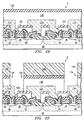
- FIGURE 2B illustrates patterning of resist 110 to form interconnects to contacts 80. Successive or simultaneous etching of nitride 102 and oxide 100 forms etch regions 112. Depending on the critical dimension dictated by the fabrication equipment, patterning of resist 110 can withstand a certain amount of degradation and alignment margin or tolerance while still forming an interconnect with suitable electrical characteristics. Referring specifically to etched region 112 overlying contact 80, a first portion of etched region 112 terminates on conductive layer 70 and a second portion of etched region 112 terminates on a non-conductive layer, such as stopping layer 36 or sidewalls 38 of gate 22. Therefore, resist 110 may be patterned to form etched region 112 to expose portions of contact 80 and portions of adjacent gates 20 or 22 while still providing an effective contact to source/drain region 40. It should be understood that resist 110 may be patterned to accomplish any particular component design in device 2.
- FIGURE 2C illustrates device 2 after forming a metal 114, such as aluminum or tungsten, in etched regions 112.
- Oxide/nitride isolation structures 116 formed above in FIGURE 2B, are disposed between contacts 80.
- a patterned resist 120 shown in FIGURE 2D allows etching of selected portions of metal layer 114. In this particular embodiment, the process forms a local interconnect by providing portions of metal layer 114 to electrically couple contacts 82 and 84. It should be understood that resist 120 may be patterned to accomplish any particular component design in device 2.
- FIGURE 2E illustrates similar process steps as FIGURE 2A to form another oxide layer 130 and stopping layer 132.
- a patterned resist 140 allows successive or simultaneous removal of portions of oxide layer 130 and stopping layer 132 to form oxide/nitride isolation structures 134. It should be understood that resist 140 may be patterned to accomplish any particular component design in device 2.
- FIGURE 2G illustrates device 2 after depositing metal layer 150.
- metal layer 114 couples source/drain regions 42 and 44 and metal layer 150 couples source/drain regions 40 and 46.
Landscapes
- Metal-Oxide And Bipolar Metal-Oxide Semiconductor Integrated Circuits (AREA)
- Semiconductor Memories (AREA)
- Internal Circuitry In Semiconductor Integrated Circuit Devices (AREA)
Applications Claiming Priority (2)
| Application Number | Priority Date | Filing Date | Title |
|---|---|---|---|
| US3280396P | 1996-12-09 | 1996-12-09 | |
| US32803P | 1996-12-09 |
Publications (1)
| Publication Number | Publication Date |
|---|---|
| EP0847080A1 true EP0847080A1 (fr) | 1998-06-10 |
Family
ID=21866886
Family Applications (1)
| Application Number | Title | Priority Date | Filing Date |
|---|---|---|---|
| EP97309908A Ceased EP0847080A1 (fr) | 1996-12-09 | 1997-12-09 | Améliorations dans et concernant des dispositifs semi-conducteurs |
Country Status (3)
| Country | Link |
|---|---|
| US (1) | US6214658B1 (fr) |
| EP (1) | EP0847080A1 (fr) |
| JP (1) | JPH10199991A (fr) |
Families Citing this family (6)
| Publication number | Priority date | Publication date | Assignee | Title |
|---|---|---|---|---|
| KR100712493B1 (ko) * | 2001-06-28 | 2007-04-27 | 삼성전자주식회사 | 반도체 소자 및 그 제조방법 |
| TW518719B (en) * | 2001-10-26 | 2003-01-21 | Promos Technologies Inc | Manufacturing method of contact plug |
| US7098114B1 (en) * | 2004-06-22 | 2006-08-29 | Integrated Device Technology, Inc. | Method for forming cmos device with self-aligned contacts and region formed using salicide process |
| CN101621030B (zh) * | 2008-07-02 | 2011-01-12 | 中芯国际集成电路制造(上海)有限公司 | 具有多晶硅接触的自对准mos结构 |
| JP5991729B2 (ja) * | 2011-10-07 | 2016-09-14 | キヤノン株式会社 | 固体撮像装置の製造方法 |
| US12218057B2 (en) * | 2021-04-27 | 2025-02-04 | Taiwan Semiconductor Manufacturing Company, Ltd. | Integrated circuit with backside interconnections and method of making same |
Citations (8)
| Publication number | Priority date | Publication date | Assignee | Title |
|---|---|---|---|---|
| JPS62291176A (ja) * | 1986-06-11 | 1987-12-17 | Hitachi Ltd | 半導体装置の製造方法 |
| EP0302383A1 (fr) * | 1987-08-05 | 1989-02-08 | Siemens Aktiengesellschaft | Procédé de fabrication de contacts avec une résistance basse, dans des dispositifs à semi-conducteur |
| EP0517408A1 (fr) * | 1991-06-03 | 1992-12-09 | STMicroelectronics, Inc. | Cellule et structure Sram avec des dispositifs de charge polycristallins à canal p |
| US5227319A (en) * | 1985-02-08 | 1993-07-13 | Kabushiki Kaisha Toshiba | Method of manufacturing a semiconductor device |
| EP0645820A2 (fr) * | 1993-09-20 | 1995-03-29 | Fujitsu Limited | Dispositif à semi-conducteur et son procédé de fabrication |
| US5432105A (en) * | 1994-09-19 | 1995-07-11 | United Microelectronics Corporation | Method for fabricating self-aligned polysilicon contacts on FET source/drain areas |
| JPH07263567A (ja) * | 1994-03-22 | 1995-10-13 | Nec Corp | 半導体装置の製造方法 |
| EP0738005A2 (fr) * | 1995-04-11 | 1996-10-16 | STMicroelectronics, Inc. | Procédé de fabrication d'un plat de contact dans un circuit intégré |
Family Cites Families (13)
| Publication number | Priority date | Publication date | Assignee | Title |
|---|---|---|---|---|
| US4966868A (en) * | 1988-05-16 | 1990-10-30 | Intel Corporation | Process for selective contact hole filling including a silicide plug |
| US5006911A (en) * | 1989-10-02 | 1991-04-09 | Motorola, Inc. | Transistor device with high density contacts |
| KR100199258B1 (ko) * | 1990-02-09 | 1999-06-15 | 가나이 쓰도무 | 반도체집적회로장치 |
| US5242847A (en) * | 1992-07-27 | 1993-09-07 | North Carolina State University At Raleigh | Selective deposition of doped silion-germanium alloy on semiconductor substrate |
| JP3771283B2 (ja) * | 1993-09-29 | 2006-04-26 | 株式会社ルネサステクノロジ | 半導体集積回路装置 |
| DE4435461C2 (de) * | 1993-10-06 | 2001-09-20 | Micron Technology Inc N D Ges | Dünnfilmtransistor und dessen Herstellverfahren |
| JP2591446B2 (ja) * | 1993-10-18 | 1997-03-19 | 日本電気株式会社 | 半導体装置およびその製造方法 |
| US5395787A (en) * | 1993-12-01 | 1995-03-07 | At&T Corp. | Method of manufacturing shallow junction field effect transistor |
| US5413957A (en) * | 1994-01-24 | 1995-05-09 | Goldstar Electron Co., Ltd. | Method for fabricating MOS transistor having source/drain region of shallow junction and silicide film |
| JP2978736B2 (ja) * | 1994-06-21 | 1999-11-15 | 日本電気株式会社 | 半導体装置の製造方法 |
| US5510296A (en) * | 1995-04-27 | 1996-04-23 | Vanguard International Semiconductor Corporation | Manufacturable process for tungsten polycide contacts using amorphous silicon |
| US5718800A (en) * | 1995-11-08 | 1998-02-17 | Micron Technology, Inc. | Self-aligned N+/P+ doped polysilicon plugged contacts to N+/P+ doped polysilicon gates and to N+/P+ doped source/drain regions |
| US5721146A (en) * | 1996-04-29 | 1998-02-24 | Taiwan Semiconductor Manufacturing Company Ltd | Method of forming buried contact architecture within a trench |
-
1997
- 1997-12-09 JP JP9339041A patent/JPH10199991A/ja active Pending
- 1997-12-09 EP EP97309908A patent/EP0847080A1/fr not_active Ceased
- 1997-12-09 US US08/987,507 patent/US6214658B1/en not_active Expired - Lifetime
Patent Citations (8)
| Publication number | Priority date | Publication date | Assignee | Title |
|---|---|---|---|---|
| US5227319A (en) * | 1985-02-08 | 1993-07-13 | Kabushiki Kaisha Toshiba | Method of manufacturing a semiconductor device |
| JPS62291176A (ja) * | 1986-06-11 | 1987-12-17 | Hitachi Ltd | 半導体装置の製造方法 |
| EP0302383A1 (fr) * | 1987-08-05 | 1989-02-08 | Siemens Aktiengesellschaft | Procédé de fabrication de contacts avec une résistance basse, dans des dispositifs à semi-conducteur |
| EP0517408A1 (fr) * | 1991-06-03 | 1992-12-09 | STMicroelectronics, Inc. | Cellule et structure Sram avec des dispositifs de charge polycristallins à canal p |
| EP0645820A2 (fr) * | 1993-09-20 | 1995-03-29 | Fujitsu Limited | Dispositif à semi-conducteur et son procédé de fabrication |
| JPH07263567A (ja) * | 1994-03-22 | 1995-10-13 | Nec Corp | 半導体装置の製造方法 |
| US5432105A (en) * | 1994-09-19 | 1995-07-11 | United Microelectronics Corporation | Method for fabricating self-aligned polysilicon contacts on FET source/drain areas |
| EP0738005A2 (fr) * | 1995-04-11 | 1996-10-16 | STMicroelectronics, Inc. | Procédé de fabrication d'un plat de contact dans un circuit intégré |
Non-Patent Citations (2)
| Title |
|---|
| PATENT ABSTRACTS OF JAPAN vol. 012, no. 187 (E - 615) 31 May 1988 (1988-05-31) * |
| PATENT ABSTRACTS OF JAPAN vol. 096, no. 002 29 February 1996 (1996-02-29) * |
Also Published As
| Publication number | Publication date |
|---|---|
| JPH10199991A (ja) | 1998-07-31 |
| US6214658B1 (en) | 2001-04-10 |
Similar Documents
| Publication | Publication Date | Title |
|---|---|---|
| US5472897A (en) | Method for fabricating MOS device with reduced anti-punchthrough region | |
| US5736419A (en) | Method of fabricating a raised source/drain MOSFET using self-aligned POCl3 for doping gate/source/drain regions | |
| US6124189A (en) | Metallization structure and method for a semiconductor device | |
| US5346836A (en) | Process for forming low resistance contacts between silicide areas and upper level polysilicon interconnects | |
| US5899719A (en) | Sub-micron MOSFET | |
| US4622735A (en) | Method for manufacturing a semiconductor device utilizing self-aligned silicide regions | |
| US5933741A (en) | Method of making titanium silicide source/drains and tungsten silicide gate electrodes for field effect transistors | |
| US5786255A (en) | Method of forming a metallic oxide semiconductor | |
| KR19980064586A (ko) | 반도체 장치 및 그 제조 방법 | |
| US5981383A (en) | Method of fabricating a salicide layer of a device electrode | |
| JPH05347273A (ja) | 集積回路の部分内部配線導体の製造法 | |
| US6214656B1 (en) | Partial silicide gate in sac (self-aligned contact) process | |
| EP0054259B1 (fr) | Procédé de fabrication d'un dispositif semiconducteur du type MIS | |
| US5882964A (en) | Process for the production of an integrated CMOS circuit | |
| US20020001935A1 (en) | Method of forming gate electrode in semiconductor device | |
| US5081065A (en) | Method of contacting silicide tracks | |
| US6100569A (en) | Semiconductor device with shared contact | |
| US6150223A (en) | Method for forming gate spacers with different widths | |
| US20030124844A1 (en) | Method to form self-aligned silicide with reduced sheet resistance | |
| US6214658B1 (en) | Self-aligned contact structure and method | |
| US5858846A (en) | Salicide integration method | |
| US6127214A (en) | Contact gate structure and method | |
| KR100212455B1 (ko) | 이중 게이트 구조의 반도체 소자 제조 방법 | |
| US5843834A (en) | Self-aligned POCL3 process flow for submicron microelectronics applications using amorphized polysilicon | |
| US6043116A (en) | Method of fabricating self-align-contact |
Legal Events
| Date | Code | Title | Description |
|---|---|---|---|
| PUAI | Public reference made under article 153(3) epc to a published international application that has entered the european phase |
Free format text: ORIGINAL CODE: 0009012 |
|
| AK | Designated contracting states |
Kind code of ref document: A1 Designated state(s): DE FR GB IT NL |
|
| AX | Request for extension of the european patent |
Free format text: AL;LT;LV;MK;RO;SI |
|
| 17P | Request for examination filed |
Effective date: 19981027 |
|
| AKX | Designation fees paid |
Free format text: DE FR GB IT NL |
|
| RBV | Designated contracting states (corrected) |
Designated state(s): DE FR GB IT NL |
|
| 17Q | First examination report despatched |
Effective date: 20031223 |
|
| 17Q | First examination report despatched |
Effective date: 20031223 |
|
| STAA | Information on the status of an ep patent application or granted ep patent |
Free format text: STATUS: THE APPLICATION HAS BEEN REFUSED |
|
| 18R | Application refused |
Effective date: 20090707 |