EP0847083A2 - Méthode de fabrication d'un condensateur pour un dispositif à semi-conducteur - Google Patents
Méthode de fabrication d'un condensateur pour un dispositif à semi-conducteur Download PDFInfo
- Publication number
- EP0847083A2 EP0847083A2 EP97306270A EP97306270A EP0847083A2 EP 0847083 A2 EP0847083 A2 EP 0847083A2 EP 97306270 A EP97306270 A EP 97306270A EP 97306270 A EP97306270 A EP 97306270A EP 0847083 A2 EP0847083 A2 EP 0847083A2
- Authority
- EP
- European Patent Office
- Prior art keywords
- layer pattern
- diffusion barrier
- barrier layer
- forming
- conductive layer
- Prior art date
- Legal status (The legal status is an assumption and is not a legal conclusion. Google has not performed a legal analysis and makes no representation as to the accuracy of the status listed.)
- Granted
Links
Images

Classifications
-
- H—ELECTRICITY
- H10—SEMICONDUCTOR DEVICES; ELECTRIC SOLID-STATE DEVICES NOT OTHERWISE PROVIDED FOR
- H10B—ELECTRONIC MEMORY DEVICES
- H10B12/00—Dynamic random access memory [DRAM] devices
-
- H—ELECTRICITY
- H10—SEMICONDUCTOR DEVICES; ELECTRIC SOLID-STATE DEVICES NOT OTHERWISE PROVIDED FOR
- H10W—GENERIC PACKAGES, INTERCONNECTIONS, CONNECTORS OR OTHER CONSTRUCTIONAL DETAILS OF DEVICES COVERED BY CLASS H10
- H10W20/00—Interconnections in chips, wafers or substrates
- H10W20/01—Manufacture or treatment
- H10W20/031—Manufacture or treatment of conductive parts of the interconnections
- H10W20/032—Manufacture or treatment of conductive parts of the interconnections of conductive barrier, adhesion or liner layers
- H10W20/033—Manufacture or treatment of conductive parts of the interconnections of conductive barrier, adhesion or liner layers in openings in dielectrics
- H10W20/037—Manufacture or treatment of conductive parts of the interconnections of conductive barrier, adhesion or liner layers in openings in dielectrics the barrier, adhesion or liner layers being on top of a main fill metal
-
- H—ELECTRICITY
- H10—SEMICONDUCTOR DEVICES; ELECTRIC SOLID-STATE DEVICES NOT OTHERWISE PROVIDED FOR
- H10D—INORGANIC ELECTRIC SEMICONDUCTOR DEVICES
- H10D1/00—Resistors, capacitors or inductors
- H10D1/60—Capacitors
- H10D1/68—Capacitors having no potential barriers
- H10D1/692—Electrodes
-
- H—ELECTRICITY
- H10—SEMICONDUCTOR DEVICES; ELECTRIC SOLID-STATE DEVICES NOT OTHERWISE PROVIDED FOR
- H10W—GENERIC PACKAGES, INTERCONNECTIONS, CONNECTORS OR OTHER CONSTRUCTIONAL DETAILS OF DEVICES COVERED BY CLASS H10
- H10W20/00—Interconnections in chips, wafers or substrates
- H10W20/01—Manufacture or treatment
- H10W20/031—Manufacture or treatment of conductive parts of the interconnections
- H10W20/032—Manufacture or treatment of conductive parts of the interconnections of conductive barrier, adhesion or liner layers
- H10W20/038—Manufacture or treatment of conductive parts of the interconnections of conductive barrier, adhesion or liner layers covering conductive structures
-
- H—ELECTRICITY
- H10—SEMICONDUCTOR DEVICES; ELECTRIC SOLID-STATE DEVICES NOT OTHERWISE PROVIDED FOR
- H10W—GENERIC PACKAGES, INTERCONNECTIONS, CONNECTORS OR OTHER CONSTRUCTIONAL DETAILS OF DEVICES COVERED BY CLASS H10
- H10W20/00—Interconnections in chips, wafers or substrates
- H10W20/01—Manufacture or treatment
- H10W20/031—Manufacture or treatment of conductive parts of the interconnections
- H10W20/032—Manufacture or treatment of conductive parts of the interconnections of conductive barrier, adhesion or liner layers
- H10W20/046—Manufacture or treatment of conductive parts of the interconnections of conductive barrier, adhesion or liner layers the barrier, adhesion or liner layers being associated with interconnections of capacitors
-
- H—ELECTRICITY
- H10—SEMICONDUCTOR DEVICES; ELECTRIC SOLID-STATE DEVICES NOT OTHERWISE PROVIDED FOR
- H10B—ELECTRONIC MEMORY DEVICES
- H10B12/00—Dynamic random access memory [DRAM] devices
- H10B12/01—Manufacture or treatment
- H10B12/02—Manufacture or treatment for one transistor one-capacitor [1T-1C] memory cells
- H10B12/03—Making the capacitor or connections thereto
- H10B12/033—Making the capacitor or connections thereto the capacitor extending over the transistor
- H10B12/0335—Making a connection between the transistor and the capacitor, e.g. plug
-
- H—ELECTRICITY
- H10—SEMICONDUCTOR DEVICES; ELECTRIC SOLID-STATE DEVICES NOT OTHERWISE PROVIDED FOR
- H10D—INORGANIC ELECTRIC SEMICONDUCTOR DEVICES
- H10D1/00—Resistors, capacitors or inductors
- H10D1/60—Capacitors
- H10D1/68—Capacitors having no potential barriers
- H10D1/692—Electrodes
- H10D1/694—Electrodes comprising noble metals or noble metal oxides
Definitions
- the present invention relates to a method for manufacturing a capacitor for a semiconductor device, and more particularly, to a method for manufacturing a lower electrode of a capacitor to which a thin film having a high dielectric constant is applied.
- the decrease of cell capacitance along with a decrease in the area of a memory cell places a serious obstacle in increasing the integration level of DRAMs.
- the decrease of cell capacitance impedes the operation of a device at a low voltage as well as lowering the reading ability of a memory cell and increasing the soft error rate.
- the capacitance should be increased.
- the effective area of a capacitor is A
- a dielectric constant in vacuum is ⁇ 0
- the relative dielectric constant of a dielectric ⁇ r is the thickness of the dielectric
- the capacitance C is given as A ⁇ 0 ⁇ r /d. Therefore, the capacitor capacitance C increases with a larger effective area A, a larger effective constant ⁇ r of a dielectric layer, and a smaller thickness d of the dielectric layer.
- three-dimensional lower electrode structures such as fin, box, and cylindrical structures have been suggested.
- a capacitor having the thin film of high dielectric constant is more preferred in terms of the high integration level of semiconductor devices as well as process simplication, because a capacitor to which a thin film having a high dielectric constant is applied can secure a sufficient capacitance with a simple two-dimensional lower electrode.
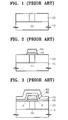
- FIGS. 1, 2, and 3 are sectional views for explaining a conventional method for manufacturing a capacitor for a semiconductor device.
- FIG. 1 illustrates the step of forming an interlayer insulating layer pattern 20 and a contact plug 30.
- the interlayer insulating layer pattern 20 is formed on a semiconductor substrate 10 to have a contact hole exposing a predetermined area of the semiconductor substrate 10.
- an impurity-doped polysilicon layer is formed on the resultant structure having the interlayer insulating layer pattern 20, to fill the contact hole.
- the contact plug 30 is formed in the contact hole by completing etching the polysilicon layer till the interlayer insulating layer pattern 20 is exposed.
- FIG. 2 illustrates the step of completing a lower electrode constituted of the contact plug 30, a diffusion barrier layer pattern 40, and a conductive layer pattern 50 by forming the diffusion barrier layer 40 and the conductive layer pattern 50.
- a diffusion barrier layer and a conductive layer are sequentially formed of a titanium nitride (TiN) and platinum (Pt), respectively, on the resultant structure having the contact plug 30 formed therein.
- the diffusion barrier layer pattern 40 and the conductive layer pattern 50 are formed to be sequentially stacked on the contact plug 30 by sequentially etching the conductive layer and the diffusion barrier layer till the interlayer insulating layer pattern 20 is exposed. That is, the lower electrode is completed, which has the contact plug 30, the diffusion barrier layer pattern 40, and the conductive layer pattern 50.
- the diffusion barrier layer pattern 40 serves to prevent the capacitance of a capacitor from decreasing due to reaction between the contact plug 30 and the conductive layer pattern 50 in a subsequent dielectric forming process.
- FIG. 3 illustrates the step of completing the capacitor by forming a dielectric layer 60 and an upper electrode 70.
- an amorphous dielectric layer containing Ba, Sr, Ti, and O is formed on the resultant having the lower electrode formed thereon by chemical vapor deposition (CVD) or sputtering.
- the resultant including the amorphous dielectric layer is heat-treated at 500-750°C so that the amorphous dielectric layer is crystallized.
- a crystalline dielectric layer 60 is formed of (Ba, Sr)TiO 2 of a perovskite structure.
- the crystalline dielectric layer 60 is referred to as the dielectric layer 60, hereinafter.
- the dielectric layer 60 can be formed in an in-situ method where materials respectively containing Ba, Sr, Ti, and O are deposited on the resultant including the lower electrode, while the resultant including the lower electrode is being heat-treated at 500-750°C. Then, the upper electrode 70 is formed on the dielectric layer 60, thus completing the capacitor.
- the dielectric forming step is necessarily accompanied by the above-described heat treatment. Since a sidewall A of the diffusion barrier layer pattern 40 makes contact with the amorphous dielectric layer containing oxygen, the oxygen penetrates into the sidewall A of the diffusion barrier layer pattern 40 during the heat treatment, thus oxidizing the diffusion barrier layer pattern 40 and the contact plug 30. That is, materials having a low dielectric constants such as TiO 2 and SiO 2 are formed.
- the diffusion barrier layer pattern 40 and the contact plug 30 are also oxidized because the sidewall of the diffusion barrier layer pattern 40 is exposed to an oxygen atmosphere.
- the diffusion barrier layer pattern 40 and the contact plug 30 are likely to be oxidized by oxygen penetrating into the diffusion barrier layer pattern 40 through the conductive layer pattern 40.
- the diffusion barrier layer pattern 40 prevents the contact plug 30 and the conductive layer pattern 50 from reacting at their interface, oxygen penetrating into the sidewall of the diffusion barrier layer pattern 40 and the conductive layer pattern 50 during the step of forming the dielectric layer 60 oxidizes the diffusion barrier layer pattern 40 and the contact plug 30, thus producing materials of low dielectric constants such as TiO 2 and SiO 2 . As a result, the capacitance of the capacitor is remarkably reduced.
- a method of manufacturing a capacitor for a semiconductor device comprises the steps of:
- the contact plug may be formed of one selected from a group consisting of impurity-doped polysilicon, tungsten (W), tungsten nitride (WN), and tungsten silicide (Wsix), and the diffusion barrier layer pattern formed of one selected from a group consisting of Ta, Co, TiN, (Ti, Al)N, (Ti, Si)N, TaN, (Ta, Si)N, TiSix, TaSix, and CoSiX.
- the conductive layer pattern may be formed of one selected from a group consisting of platinum (Pt), iridium (Ir), ruthenium (Ru), iridium dioxide (IrO 2 ), and ruthenium dioxide (RuO 2 ), and the contact plug, the diffusion barrier layer pattern, and the conductive layer pattern formed of impurity-doped polysilicon, titanium nitride (TiN), and platinum (Pt), respectively.
- a method of manufacturing a capacitor for a semmiconductor device comprises the steps of:
- the contact plug may be formed of one selected from a group consisting of impurity-doped polysilicon, tungsten (W), tungsten nitride (WN) , and tungsten silicide (Wsix), and the first diffusion barrier layer pattern formed of one selected from a group consisting of Ta, Co, TiN, (Ti, Al)N, (Ti, Si)N, TaN, (Ta, Si)N, TiSix, TaSix, and CoSix.
- the second diffusion barrier layer pattern may be formed of one selected from a group consisting of Ir, Ru, IrO 2 , and RUO 2 , and the conductive layer pattern formed of Pt.
- the second diffusion barrier layer may be formed to have a double-layer structure where Ir and IrO2 are sequentially stacted, and the conductive layer pattern is formed of Pt.
- the method of manufacturing a capacitor for a semiconductor device according to the present invention prevents reduction of the capacitance of the capacitor due to oxidation of a portion of the lower electrode by preventing oxidation of the diffusion barrier layer pattern.
- FIG. 4 illustrates the step of forming a first interlayer insulating layer pattern 120, a contact plug 130, and a diffusion barrier layer pattern 140.
- the first interlayer insulating layer pattern 120 is formed on a semiconductor substrate 110 to have a first contact hole exposing a predetermined area of the semiconductor substrate 110.
- a first conductive layer is formed on the resultant including the first interlayer insulating layer pattern 120, to fill the first contact hole.
- the first conductive layer is formed of impurity-doped polysilicon, tungsten (W), tungsten nitride (WN), or tungsten silicide (WSix).
- the contact plug 130 is formed in the first contact hole by completly etching the first conductive layer till the first interlayer insulating layer pattern 120 is exposed.
- a diffusion barrier layer is formed of Ta, Co, TiN, (Ti, Al)N, (Ti, Si)N, TaN, (Ta, Si)N, TiSix, TaSix, or CoSix on the resultant including the contact plug 130.
- the diffusion barrier layer serves to prevent reaction between the contact plug 130 and a conductive layer pattern 150 of FIG. 5.
- the diffusion barrier layer pattern 140 is formed on the contact plug 130 by etching the diffusion barrier layer till the first interlayer insulating layer pattern 120 is exposed.
- FIG. 5 illustrates the step of forming a second interlayer insulating layer pattern 145 and a conductive layer pattern 150, thus completing a lower electrode having the contact plug 130, the diffusion barrier layer pattern 140, and the conductive layer pattern 150.
- a second interlayer insulating layer is formed on the resultant including the diffusion barrier layer pattern 140. Then, the second interlayer insulating layer pattern 145 is formed to have a second contact hole by etching the second interlayer insulating layer till the diffusion barrier layer pattern 140 is exposed.
- a second conductive layer is formed of platinum (Pt), iridium (Ir), ruthenium(Ru), iridium dioxide (IrO 2 ), or ruthenium dioxide (RuO 2 ).
- the conductive layer pattern 150 is formed on the second interlayer insulating layer pattern 145 to make contact with the diffusion barrier layer pattern 140 through the second contact hole by patterning the second conductive layer till the second interlayer insulating layer pattern 145 is exposed. That is, the lower electrode having the contact plug 130, the diffusion barrier layer pattern 140, and the conductive layer pattern 150 is completed.
- FIG. 6 illustrates the step of completing the capacitor of the present invention by forming a dielectric layer 160 and an upper electrode 170.
- an amorphous dielectric layer is formed on the resultant having the completed lower electrode thereon.
- the resultant is heat-treated to crystallize the amorphous dielectric layer, thus forming a crystalline dielectric layer 160 of SrTiO 3 , (BaSr)TiO 3 , (Pb, Zr)TiO 3 , or (Pb, Zr)(Ti, La)TiO 3 .
- the crystalline dielectric layer 160 may be formed in in-situ, while the resultant including the lower electrode is heat-treated.
- the crystalline dielectric layer 160 is referred to as the dielectric layer 160, hereinafter.
- the upper electrode 170 is formed on the dielectric layer 160, thus completing the capacitor of the present invention.
- the diffusion barrier layer pattern 140 does not contact with the amorphous dielectric layer, oxygen cannot react with the diffusion barrier layer pattern 140 during the heat treatment, in contrast to the prior art. Therefore, oxidation of the diffusion barrier layer pattern 140 and the contact plug 130 is prevented.
- the dielectric layer 160 is formed in in-situ, oxidation of the diffusion barrier layer pattern 142 and the contact plug 130 can be also prevented because the diffusion barrier layer pattern 142 is not exposed to an oxygen atmosphere.
- the second interlayer insulating layer 145 is thin based on its surface, it takes a larger amount time for oxygen to reach the diffusion barrier layer pattern 140 through the conductive layer pattern 150 because the conductive layer pattern 150 contacts the diffusion barrier layer pattern 140 through the second contact hole. Accordingly, oxidation of the diffusion barrier layer pattern 140 due to oxygen introduced through the conductive layer pattern 150 can be prevented.
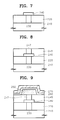
- FIGS. 7, 8, and 9 are sectional views for explaining a method for manufacturing a capacitor for a semiconductor device according to a second embodiment of the present invention.
- FIG. 7 illustrates the step of forming a first interlayer insulating layer pattern 220, a contact plug 230, and a first diffusion barrier layer pattern 140.
- the first interlayer insulating layer pattern 220 is formed on a semiconductor substrate 210 to have a first contact hole exposing a predetermined area of the semiconductor substrate 210.
- a first conductive layer is formed of impurity-dope polysilicon, tungsten (W), tungsten nitride (WN), or tungsten silicide (Wsix) to fill the first contact hole, on the resultant including the first interlayer insulating layer pattern 220.
- the contact plug 230 is formed in the first contact hole by completly etching the first conductive layer till the first interlayer insulating layer pattern 220 is exposed.
- a first diffusion barrier layer is formed of Ta, Co, TiN, (Ti, Al)N, (Ti, Si)N, TaN, (Ta, Si)N, TiSix, TaSix, or CoSix on the resultant including the contact plug 230.
- the first diffusion barrier layer serves to prevent reaction between the contact plug 230 and a second diffusion barrier layer pattern 247 of FIG. 8. Then, the first diffusion barrier layer pattern 240 is formed on the contact plug 230 by etching the first diffusion barrier layer till the interlayer insulating layer pattern 245 is exposed.
- FIG. 8 illustrates the step of forming a second interlayer insulating layer 245 and a second diffusion barrier layer pattern 247.
- a second interlayer insulating layer is formed on the resultant including the first diffusion barrier layer pattern 240. Then, the second interlayer insulating layer pattern 245 is formed to have a second contact hole by patterning the second interlayer insulating layer till the first diffusion barrier layer pattern 240 is exposed.
- a diffusion barrier layer is formed of iridium (Ir), ruthenium (Ru), iridium dioxide (IrO 2 ), or ruthenium dioxide (RuO 2 ) to fill the second contact hole, on the second interlayer insulating layer pattern 245.
- the second diffusion barrier layer can be formed to have a double-layer structure where iridium and iridium dioxide are sequentially stacked to increase the adhesiveness between the second diffusion barrier layer and a conductive layer pattern 250 of FIG 9.
- the second diffusion barrier layer pattern 247 is formed in the second contact hole by completly etching the second diffusion barrier layer till the second interlayer insulating layer pattern 245 is exposed.
- the second diffusion barrier layer pattern 247 serves to prevent oxidation of the first diffusion barrier layer pattern 240.
- FIG. 9 illustrates the steps of completing a lower electrode including the contact plug 230, the first diffusion barrier layer pattern 240, the second diffusion barrier layer pattern 247, and the conductive layer pattern 250, and completing the capacitor of the present invention by forming a dielectric layer 260 and an upper electrode 270.
- a second conductive layer is formed on the resultant including the second diffusion barrier layer pattern 247 using platinum (Pt). Then, the conductive layer pattern 250 is formed on the second diffusion barrier layer pattern 247 by patterning the second conductive layer till the second interlayer insulating layer pattern 245 is exposed. That is, the lower electrode having the contact plug 230, the first diffusion barrier layer pattern 240, the second diffusion barrier layer pattern 247, and the conductive layer pattern 250 is completed.
- an amorphous dielectric layer is formed on the resultant having the completed lower electrode thereon.
- the resultant including the amorphous dielectric layer is heat-treated to crystallize the amorphous dielectric layer, thus forming a crystalline dielectric layer 260 of SrTiO 3 , (BaSr)TiO 3 , (Pb, Zr)TiO 3 , or (Pb, Zr)(Ti, La)TiO 3 .
- the crystalline dielectric layer 160 may be formed in in-situ, while the resultant including the lower electrode is heat-treated.
- the crystalline dielectric layer 260 is referred to as the dielectric layer 260, hereinafter.
- the upper electrode 270 is formed on the dielectric layer 260, thus completing the capacitor of the present invention.
- the first diffusion barrier layer pattern 240 makes no contact with the amorphous dielectric layer, oxidation of the first diffusion barrier layer pattern 240 is prevented during the heat-treatment.
- the dielectric layer 260 is formed in in-situ, oxidation of the diffusion first barrier layer pattern 240 is prevented because the first diffusion barrier layer pattern 240 is not exposed to an oxygen atmosphere.
- reaction between oxygen introduced through the conductive layer pattern 250 and the first diffusion barrier layer pattern 240 can be prevented by forming the second diffusion barrier layer pattern 247.
Landscapes
- Semiconductor Memories (AREA)
- Semiconductor Integrated Circuits (AREA)
Applications Claiming Priority (2)
| Application Number | Priority Date | Filing Date | Title |
|---|---|---|---|
| KR9661658 | 1996-12-04 | ||
| KR1019960061658A KR100219506B1 (ko) | 1996-12-04 | 1996-12-04 | 반도체장치의 커패시터 제조방법 |
Publications (3)
| Publication Number | Publication Date |
|---|---|
| EP0847083A2 true EP0847083A2 (fr) | 1998-06-10 |
| EP0847083A3 EP0847083A3 (fr) | 1998-12-23 |
| EP0847083B1 EP0847083B1 (fr) | 2006-03-22 |
Family
ID=19485692
Family Applications (1)
| Application Number | Title | Priority Date | Filing Date |
|---|---|---|---|
| EP97306270A Expired - Lifetime EP0847083B1 (fr) | 1996-12-04 | 1997-08-19 | Méthode de fabrication d'un condensateur pour un dispositif à semi-conducteur |
Country Status (4)
| Country | Link |
|---|---|
| EP (1) | EP0847083B1 (fr) |
| KR (1) | KR100219506B1 (fr) |
| DE (1) | DE69735521T2 (fr) |
| TW (1) | TW346658B (fr) |
Cited By (5)
| Publication number | Priority date | Publication date | Assignee | Title |
|---|---|---|---|---|
| EP1018767A1 (fr) * | 1998-12-10 | 2000-07-12 | Siemens Aktiengesellschaft | Sillon étendu pour empêcher l'interaction entre parties de condensateurs empilés |
| GB2368725A (en) * | 2000-06-30 | 2002-05-08 | Hynix Semiconductor Inc | A semiconductor memory device |
| US6387748B1 (en) | 1999-02-16 | 2002-05-14 | Micron Technology, Inc. | Semiconductor circuit constructions, capacitor constructions, and methods of forming semiconductor circuit constructions and capacitor constructions |
| GB2368972A (en) * | 2000-06-19 | 2002-05-15 | Hynix Semiconductor Inc | Semiconductor memory device having plug contacted to capacitor electrode |
| WO2005086231A1 (fr) * | 2004-02-27 | 2005-09-15 | Infineon Technologies Ag | Structure a semi-conducteur |
Families Citing this family (3)
| Publication number | Priority date | Publication date | Assignee | Title |
|---|---|---|---|---|
| US20010013660A1 (en) * | 1999-01-04 | 2001-08-16 | Peter Richard Duncombe | Beol decoupling capacitor |
| KR100351451B1 (ko) * | 1999-12-30 | 2002-09-09 | 주식회사 하이닉스반도체 | 반도체메모리장치의 커패시터제조방법 |
| KR20030023143A (ko) * | 2001-09-12 | 2003-03-19 | 주식회사 하이닉스반도체 | 반도체 소자 및 그 제조 방법 |
Family Cites Families (5)
| Publication number | Priority date | Publication date | Assignee | Title |
|---|---|---|---|---|
| US5335138A (en) * | 1993-02-12 | 1994-08-02 | Micron Semiconductor, Inc. | High dielectric constant capacitor and method of manufacture |
| US5392189A (en) * | 1993-04-02 | 1995-02-21 | Micron Semiconductor, Inc. | Capacitor compatible with high dielectric constant materials having two independent insulative layers and the method for forming same |
| JP2550852B2 (ja) * | 1993-04-12 | 1996-11-06 | 日本電気株式会社 | 薄膜キャパシタの製造方法 |
| US5489548A (en) * | 1994-08-01 | 1996-02-06 | Texas Instruments Incorporated | Method of forming high-dielectric-constant material electrodes comprising sidewall spacers |
| WO1996017381A1 (fr) * | 1994-11-28 | 1996-06-06 | Hitachi, Ltd. | Dispositif a semi-conducteur et son procede de production |
-
1996
- 1996-12-04 KR KR1019960061658A patent/KR100219506B1/ko not_active Expired - Fee Related
-
1997
- 1997-08-04 TW TW086111110A patent/TW346658B/zh not_active IP Right Cessation
- 1997-08-19 EP EP97306270A patent/EP0847083B1/fr not_active Expired - Lifetime
- 1997-08-19 DE DE69735521T patent/DE69735521T2/de not_active Expired - Lifetime
Cited By (17)
| Publication number | Priority date | Publication date | Assignee | Title |
|---|---|---|---|---|
| US6222220B1 (en) | 1998-12-10 | 2001-04-24 | Siemens Aktiengesellschaft | Extended trench for preventing interaction between components of stacked capacitors |
| EP1018767A1 (fr) * | 1998-12-10 | 2000-07-12 | Siemens Aktiengesellschaft | Sillon étendu pour empêcher l'interaction entre parties de condensateurs empilés |
| US6387748B1 (en) | 1999-02-16 | 2002-05-14 | Micron Technology, Inc. | Semiconductor circuit constructions, capacitor constructions, and methods of forming semiconductor circuit constructions and capacitor constructions |
| US6555863B1 (en) | 1999-02-16 | 2003-04-29 | Micron Technology, Inc. | Semiconductor circuit constructions, capacitor constructions, and methods of forming semiconductor circuit constructions and capacitor constructions |
| US6638809B2 (en) * | 1999-02-16 | 2003-10-28 | Micron Technology, Inc. | Methods of forming semiconductor circuit constructions and capacitor constructions |
| US6780792B2 (en) | 1999-02-16 | 2004-08-24 | Micron Technology, Inc. | Semiconductor circuit constructions, capacitor constructions, and methods of forming semiconductor circuit constructions and capacitor constructions |
| GB2368972B (en) * | 2000-06-19 | 2004-10-13 | Hynix Semiconductor Inc | Semiconductor memory device having plug contacted to capacitor electrode and method for fabricating the same |
| DE10130626B4 (de) * | 2000-06-19 | 2012-03-15 | Hynix Semiconductor Inc. | Verfahren zur Herstellung eines Halbleiterspeicherelements mit einem mit einer Kondensatorelektrode verbundenen Anschluss |
| GB2368972A (en) * | 2000-06-19 | 2002-05-15 | Hynix Semiconductor Inc | Semiconductor memory device having plug contacted to capacitor electrode |
| US6461913B2 (en) | 2000-06-19 | 2002-10-08 | Hynix Semiconductor Inc. | Semiconductor memory device having plug contacted to a capacitor electrode and method for fabricating a capacitor of the semiconductor memory device |
| US6734061B2 (en) | 2000-06-30 | 2004-05-11 | Hynix Semiconductor Inc. | Semiconductor memory device having a plug contacted to a capacitor electrode and method for fabricating the capacitor |
| GB2368725B (en) * | 2000-06-30 | 2004-12-08 | Hynix Semiconductor Inc | Semiconductor memory device and fabrication |
| GB2368725A (en) * | 2000-06-30 | 2002-05-08 | Hynix Semiconductor Inc | A semiconductor memory device |
| WO2005086231A1 (fr) * | 2004-02-27 | 2005-09-15 | Infineon Technologies Ag | Structure a semi-conducteur |
| US7221034B2 (en) | 2004-02-27 | 2007-05-22 | Infineon Technologies Ag | Semiconductor structure including vias |
| US7253492B2 (en) | 2004-02-27 | 2007-08-07 | Infineon Technologies Ag | Semiconductor structure with via structure |
| CN100501984C (zh) * | 2004-02-27 | 2009-06-17 | 英飞凌科技股份公司 | 半导体结构 |
Also Published As
| Publication number | Publication date |
|---|---|
| TW346658B (en) | 1998-12-01 |
| DE69735521T2 (de) | 2007-03-08 |
| EP0847083B1 (fr) | 2006-03-22 |
| EP0847083A3 (fr) | 1998-12-23 |
| KR100219506B1 (ko) | 1999-09-01 |
| KR19980043704A (ko) | 1998-09-05 |
| DE69735521D1 (de) | 2006-05-11 |
Similar Documents
| Publication | Publication Date | Title |
|---|---|---|
| US6599806B2 (en) | Method for manufacturing a capacitor of a semiconductor device | |
| US5955774A (en) | Integrated circuit ferroelectric memory devices including resistors in periphery region | |
| US6831323B2 (en) | Semiconductor device and method for fabricating the same | |
| US6020233A (en) | Ferroelectric memory device guaranteeing electrical interconnection between lower capacitor electrode and contact plug and method for fabricating the same | |
| US6078493A (en) | Fin-shaped capacitor | |
| KR100308241B1 (ko) | 반도체장치의 제조방법 | |
| US6130124A (en) | Methods of forming capacitor electrodes having reduced susceptibility to oxidation | |
| US6798010B2 (en) | Ferroelectric memory devices | |
| KR100423906B1 (ko) | 강유전성 메모리 장치 및 그 제조방법 | |
| JP2929436B2 (ja) | 半導体メモリ装置及びその製造方法 | |
| KR100235949B1 (ko) | 반도체 소자의 캐패시터 제조 방법 | |
| EP0847083B1 (fr) | Méthode de fabrication d'un condensateur pour un dispositif à semi-conducteur | |
| US6917114B2 (en) | Semiconductor device and method of fabricating the same | |
| US7042034B2 (en) | Capacitor | |
| KR19980065687A (ko) | 커패시터의 제조방법 | |
| US20030058678A1 (en) | Ferroelectric memory device and method of fabricating the same | |
| KR20000001619A (ko) | 굴곡형 컨테이너 형상의 하부전극을 갖는 반도체장치의 커패시터 및 그 제조방법 | |
| KR100687433B1 (ko) | 캐패시터의 하부전극 형성 방법 | |
| KR19990010450A (ko) | 장벽층의 산화를 방지하는 커패시터 및 그 제조 방법 | |
| KR20040059848A (ko) | 반도체 장치의 캐패시터 제조방법 |
Legal Events
| Date | Code | Title | Description |
|---|---|---|---|
| PUAI | Public reference made under article 153(3) epc to a published international application that has entered the european phase |
Free format text: ORIGINAL CODE: 0009012 |
|
| 17P | Request for examination filed |
Effective date: 19970903 |
|
| AK | Designated contracting states |
Kind code of ref document: A2 Designated state(s): DE FR GB IT |
|
| AX | Request for extension of the european patent |
Free format text: AL;LT;LV;RO;SI |
|
| PUAL | Search report despatched |
Free format text: ORIGINAL CODE: 0009013 |
|
| AK | Designated contracting states |
Kind code of ref document: A3 Designated state(s): AT BE CH DE DK ES FI FR GB GR IE IT LI LU MC NL PT SE |
|
| AX | Request for extension of the european patent |
Free format text: AL;LT;LV;RO;SI |
|
| AKX | Designation fees paid |
Free format text: DE FR GB IT |
|
| 17Q | First examination report despatched |
Effective date: 20040825 |
|
| GRAP | Despatch of communication of intention to grant a patent |
Free format text: ORIGINAL CODE: EPIDOSNIGR1 |
|
| GRAS | Grant fee paid |
Free format text: ORIGINAL CODE: EPIDOSNIGR3 |
|
| GRAA | (expected) grant |
Free format text: ORIGINAL CODE: 0009210 |
|
| AK | Designated contracting states |
Kind code of ref document: B1 Designated state(s): DE FR GB IT |
|
| REG | Reference to a national code |
Ref country code: GB Ref legal event code: FG4D |
|
| REF | Corresponds to: |
Ref document number: 69735521 Country of ref document: DE Date of ref document: 20060511 Kind code of ref document: P |
|
| ET | Fr: translation filed | ||
| PLBE | No opposition filed within time limit |
Free format text: ORIGINAL CODE: 0009261 |
|
| STAA | Information on the status of an ep patent application or granted ep patent |
Free format text: STATUS: NO OPPOSITION FILED WITHIN TIME LIMIT |
|
| 26N | No opposition filed |
Effective date: 20061227 |
|
| PGFP | Annual fee paid to national office [announced via postgrant information from national office to epo] |
Ref country code: DE Payment date: 20110803 Year of fee payment: 15 Ref country code: FR Payment date: 20110902 Year of fee payment: 15 Ref country code: GB Payment date: 20110728 Year of fee payment: 15 |
|
| PGFP | Annual fee paid to national office [announced via postgrant information from national office to epo] |
Ref country code: IT Payment date: 20110723 Year of fee payment: 15 |
|
| GBPC | Gb: european patent ceased through non-payment of renewal fee |
Effective date: 20120819 |
|
| REG | Reference to a national code |
Ref country code: FR Ref legal event code: ST Effective date: 20130430 |
|
| PG25 | Lapsed in a contracting state [announced via postgrant information from national office to epo] |
Ref country code: IT Free format text: LAPSE BECAUSE OF NON-PAYMENT OF DUE FEES Effective date: 20120819 |
|
| PG25 | Lapsed in a contracting state [announced via postgrant information from national office to epo] |
Ref country code: GB Free format text: LAPSE BECAUSE OF NON-PAYMENT OF DUE FEES Effective date: 20120819 Ref country code: DE Free format text: LAPSE BECAUSE OF NON-PAYMENT OF DUE FEES Effective date: 20130301 |
|
| PG25 | Lapsed in a contracting state [announced via postgrant information from national office to epo] |
Ref country code: FR Free format text: LAPSE BECAUSE OF NON-PAYMENT OF DUE FEES Effective date: 20120831 |
|
| REG | Reference to a national code |
Ref country code: DE Ref legal event code: R119 Ref document number: 69735521 Country of ref document: DE Effective date: 20130301 |