EP0847116A2 - Verteiler Reflektor und Halbleiterlaser mit abstimmbarer Wellenlänge - Google Patents
Verteiler Reflektor und Halbleiterlaser mit abstimmbarer Wellenlänge Download PDFInfo
- Publication number
- EP0847116A2 EP0847116A2 EP98102645A EP98102645A EP0847116A2 EP 0847116 A2 EP0847116 A2 EP 0847116A2 EP 98102645 A EP98102645 A EP 98102645A EP 98102645 A EP98102645 A EP 98102645A EP 0847116 A2 EP0847116 A2 EP 0847116A2
- Authority
- EP
- European Patent Office
- Prior art keywords
- semiconductor laser
- wavelength
- region
- distributed reflector
- optical
- Prior art date
- Legal status (The legal status is an assumption and is not a legal conclusion. Google has not performed a legal analysis and makes no representation as to the accuracy of the status listed.)
- Granted
Links
Images


Classifications
-
- G—PHYSICS
- G02—OPTICS
- G02B—OPTICAL ELEMENTS, SYSTEMS OR APPARATUS
- G02B6/00—Light guides; Structural details of arrangements comprising light guides and other optical elements, e.g. couplings
- G02B6/10—Light guides; Structural details of arrangements comprising light guides and other optical elements, e.g. couplings of the optical waveguide type
- G02B6/12—Light guides; Structural details of arrangements comprising light guides and other optical elements, e.g. couplings of the optical waveguide type of the integrated circuit kind
- G02B6/122—Basic optical elements, e.g. light-guiding paths
- G02B6/124—Geodesic lenses or integrated gratings
-
- H—ELECTRICITY
- H01—ELECTRIC ELEMENTS
- H01S—DEVICES USING THE PROCESS OF LIGHT AMPLIFICATION BY STIMULATED EMISSION OF RADIATION [LASER] TO AMPLIFY OR GENERATE LIGHT; DEVICES USING STIMULATED EMISSION OF ELECTROMAGNETIC RADIATION IN WAVE RANGES OTHER THAN OPTICAL
- H01S5/00—Semiconductor lasers
- H01S5/06—Arrangements for controlling the laser output parameters, e.g. by operating on the active medium
- H01S5/062—Arrangements for controlling the laser output parameters, e.g. by operating on the active medium by varying the potential of the electrodes
- H01S5/0625—Arrangements for controlling the laser output parameters, e.g. by operating on the active medium by varying the potential of the electrodes in multi-section lasers
- H01S5/06255—Controlling the frequency of the radiation
- H01S5/06256—Controlling the frequency of the radiation with DBR-structure
-
- H—ELECTRICITY
- H01—ELECTRIC ELEMENTS
- H01S—DEVICES USING THE PROCESS OF LIGHT AMPLIFICATION BY STIMULATED EMISSION OF RADIATION [LASER] TO AMPLIFY OR GENERATE LIGHT; DEVICES USING STIMULATED EMISSION OF ELECTROMAGNETIC RADIATION IN WAVE RANGES OTHER THAN OPTICAL
- H01S5/00—Semiconductor lasers
- H01S5/06—Arrangements for controlling the laser output parameters, e.g. by operating on the active medium
- H01S5/062—Arrangements for controlling the laser output parameters, e.g. by operating on the active medium by varying the potential of the electrodes
- H01S5/0625—Arrangements for controlling the laser output parameters, e.g. by operating on the active medium by varying the potential of the electrodes in multi-section lasers
- H01S5/06255—Controlling the frequency of the radiation
- H01S5/06258—Controlling the frequency of the radiation with DFB-structure
-
- H—ELECTRICITY
- H01—ELECTRIC ELEMENTS
- H01S—DEVICES USING THE PROCESS OF LIGHT AMPLIFICATION BY STIMULATED EMISSION OF RADIATION [LASER] TO AMPLIFY OR GENERATE LIGHT; DEVICES USING STIMULATED EMISSION OF ELECTROMAGNETIC RADIATION IN WAVE RANGES OTHER THAN OPTICAL
- H01S5/00—Semiconductor lasers
- H01S5/10—Construction or shape of the optical resonator, e.g. extended or external cavity, coupled cavities, bent-guide, varying width, thickness or composition of the active region
- H01S5/12—Construction or shape of the optical resonator, e.g. extended or external cavity, coupled cavities, bent-guide, varying width, thickness or composition of the active region the resonator having a periodic structure, e.g. in distributed feedback [DFB] lasers
-
- G—PHYSICS
- G02—OPTICS
- G02B—OPTICAL ELEMENTS, SYSTEMS OR APPARATUS
- G02B6/00—Light guides; Structural details of arrangements comprising light guides and other optical elements, e.g. couplings
- G02B6/10—Light guides; Structural details of arrangements comprising light guides and other optical elements, e.g. couplings of the optical waveguide type
- G02B6/12—Light guides; Structural details of arrangements comprising light guides and other optical elements, e.g. couplings of the optical waveguide type of the integrated circuit kind
- G02B2006/12083—Constructional arrangements
- G02B2006/12107—Grating
-
- G—PHYSICS
- G02—OPTICS
- G02B—OPTICAL ELEMENTS, SYSTEMS OR APPARATUS
- G02B6/00—Light guides; Structural details of arrangements comprising light guides and other optical elements, e.g. couplings
- G02B6/10—Light guides; Structural details of arrangements comprising light guides and other optical elements, e.g. couplings of the optical waveguide type
- G02B6/12—Light guides; Structural details of arrangements comprising light guides and other optical elements, e.g. couplings of the optical waveguide type of the integrated circuit kind
- G02B2006/12083—Constructional arrangements
- G02B2006/12121—Laser
-
- H—ELECTRICITY
- H01—ELECTRIC ELEMENTS
- H01S—DEVICES USING THE PROCESS OF LIGHT AMPLIFICATION BY STIMULATED EMISSION OF RADIATION [LASER] TO AMPLIFY OR GENERATE LIGHT; DEVICES USING STIMULATED EMISSION OF ELECTROMAGNETIC RADIATION IN WAVE RANGES OTHER THAN OPTICAL
- H01S5/00—Semiconductor lasers
- H01S5/10—Construction or shape of the optical resonator, e.g. extended or external cavity, coupled cavities, bent-guide, varying width, thickness or composition of the active region
- H01S5/12—Construction or shape of the optical resonator, e.g. extended or external cavity, coupled cavities, bent-guide, varying width, thickness or composition of the active region the resonator having a periodic structure, e.g. in distributed feedback [DFB] lasers
- H01S5/1206—Construction or shape of the optical resonator, e.g. extended or external cavity, coupled cavities, bent-guide, varying width, thickness or composition of the active region the resonator having a periodic structure, e.g. in distributed feedback [DFB] lasers having a non constant or multiplicity of periods
- H01S5/1215—Multiplicity of periods
- H01S5/1218—Multiplicity of periods in superstructured configuration, e.g. more than one period in an alternate sequence
-
- H—ELECTRICITY
- H01—ELECTRIC ELEMENTS
- H01S—DEVICES USING THE PROCESS OF LIGHT AMPLIFICATION BY STIMULATED EMISSION OF RADIATION [LASER] TO AMPLIFY OR GENERATE LIGHT; DEVICES USING STIMULATED EMISSION OF ELECTROMAGNETIC RADIATION IN WAVE RANGES OTHER THAN OPTICAL
- H01S5/00—Semiconductor lasers
- H01S5/10—Construction or shape of the optical resonator, e.g. extended or external cavity, coupled cavities, bent-guide, varying width, thickness or composition of the active region
- H01S5/12—Construction or shape of the optical resonator, e.g. extended or external cavity, coupled cavities, bent-guide, varying width, thickness or composition of the active region the resonator having a periodic structure, e.g. in distributed feedback [DFB] lasers
- H01S5/1225—Construction or shape of the optical resonator, e.g. extended or external cavity, coupled cavities, bent-guide, varying width, thickness or composition of the active region the resonator having a periodic structure, e.g. in distributed feedback [DFB] lasers with a varying coupling constant along the optical axis
Definitions
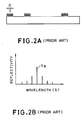
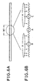
- a distributed reflector as shown in Fig. 2A which enables wavelength tuning within the range on the order of above 10 nm, which is referred to herein as reflector according to a second-conventional example.
- Fig. 2A broken line indicates portions whose depiction has been omitted.
- the waveguide has a diffractive grating of a pitch of ⁇ formed partially and periodically, thereby giving a plurality of reflection peaks in the vicinity of Bragg wavelength, ⁇ B , which depends on the pitch, ⁇ , as illustrated in Fig. 2B.
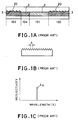
- a distributed feed back semiconductor laser having an optical waveguide comprising: an active waveguide layer defining an active region having a refractive index, an inactive waveguide layer optically connected to the active waveguide layer, defining an inactive region, a diffractive grating provided in at least a portion of the active region; a distributed reflector constituted by the diffractive grating, the active region and the inactive region; the active region having an optical gain to light having a wavelength which the distributed reflector reflects; the active region having an optical amplification action and the distributed reflector having a reflection action, and together causing lasing at least one of reflection wavelengths in the distributed reflector; the diffractive grating in the at least one distributed reflector having a plurality of repeating unit regions each having a constant length, thus forming a modulation period, and at least one parameter the determines an optical reflectivity of the diffractive grating varying depending on its position in each of the repeating unit regions along a
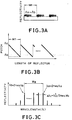
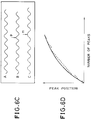
- a grating having a larger pitch than that of the portion A is formed for only a single pitch in a central position thereof. Peak positions of the diffractive grating after this point (toward the right hand side) are shifted rearward (toward the right hand side) as compared with those of the diffractive grating in the portion A in contrast to the case of the portion B. As a result of this phase shift, effects can be obtained which are equivalent to those obtainable with a larger pitch of the diffractive grating.
- the spacing at which phase shifts are inserted varies depending on their position in each repeating unit region as illustrated in Fig. 6B.
- the grating since the grating has generally a constant pitch and it is sufficient to insert phase shifts partly or at only selected positions, time required for forming a pattern of diffractive grating using electron beams can be reduced considerably as compared with the diffractive grating of the reflector 1 in which the pitch varies.
- the distributed feed back type semiconductor laser of the present invention may include two sets of comb-shaped electrodes above the front and rear distributed reflectors, and current may similarly be injected to each of the comb-shaped electrodes independently, with varying its intensity.
- the average equivalent refractive indices of the front and rear distributed reflectors can be changed independently so that lasing can occur at a wavelength in the vicinity of any selected wavelength ⁇ i .
- Simultaneous change in the average refractive indices of the front and rear distributed reflectors by the same amount makes it possible to conduct fine adjustment of lasing wavelength around the aforementioned wavelength ⁇ i .
- lasing can occur at any desired wavelength in a band ranging from wavelengths ⁇ 1 to ⁇ n .
- setting the wavelengths ⁇ 1 to ⁇ n , ⁇ ' 1 to ⁇ ' n , and ⁇ '' 1 to ⁇ '' n , at values such that gain band of the semiconductor laser can be covered enables lasing at any desired wavelength within the range of the gain band.
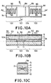
- the individual electrodes (teeth) 90 of the comb-shaped electrodes 9c and 9d for the front distributed reflector region 102 are arranged at a period of 75 ⁇ m and the width w 1 of a single tooth 90 is about half this period (about 37.5 ⁇ m).
- the individual electrodes (teeth) 90 of the comb-shaped electrodes 9e and 9f are arranged at a period of 67.5 ⁇ m and the width w 2 of a single tooth 90 is about half this period (about 33.75 ⁇ m).
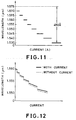
- Fig. 12 is a graph illustrating relationship between variation of lasing wavelength and current. Solid lines in Fig. 12 represent behavior of wavelength when the current applied to the aforementioned short-circuited comb-shaped electrodes 9d and 9f varies. As illustrated in Fig. 12, with the distributed reflector type semiconductor laser, simultaneous application of current to the short-circuited comb-shaped electrodes 9d and 9f results in change in lasing wavelength by about 50 ⁇ with a leap in wavelength.
- Adjustment of the currents applied to the p-type electrodes 9b to 9f, respectively, by the aforementioned procedure, enables coarse adjustment and fine adjustment of the lasing wavelength and selection of any desired lasing wavelength from over entire bandwidth of 450 ⁇ .
- the pitch modulation period of the diffractive grating is the same as that at which the individual electrodes or teeth of the comb-shaped electrodes are arranged.
- the period of repetition of the individual electrodes of the comb-shaped electrodes is smaller than the pitch modulation period of the diffractive grating, similar effects can be obtained as Examples 1 and 2 above.
- the former is larger than the latter, different effects can be obtained.
- explanation will be made hereinbelow as to how to control lasing wavelength of a semiconductor laser which has the same structure as the wavelength-tunable semiconductor laser described in Example 2 as shown in Figs. 10A to 10C except that the widths of the individual electrodes of the comb-shaped electrodes 9c to 9f are twice as large as in the case of Example 2.
- a wavelength-tunable distributed reflector type semiconductor laser according to a sixth example of the present invention will be described below.
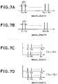
- Figs. 13A to 13C each illustrate reflectivity characteristics of the distributed reflector region of the semiconductor laser according to the instant example.
- the reflectivity characteristics of the distributed reflector region are as illustrated in Fig. 13A. That is, reflectivity peaks appear periodically at a wavelength spacing ⁇ f approximately defined by the pitch modulation period M f of the diffractive grating.
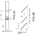
- the distributed reflector includes a substrate(1) and at least one optical waveguide formed on the substrate and having a refractive index larger than the substrate and at least one optical confinement layer(3) having a refractive index smaller than the optical waveguide layer.
- a diffractive grating(10a or 10b) is formed in at least one layer(2 or 3) constituting the optical waveguide.
- the diffractive grating has a structure of which at least one parameter defining optical reflectivity varies depending on its position, and is formed continuously for at least two periods, the period being approximately defined by the length of repeating unit region.
- the parameter may be pitch, coupling coefficient, bandgap composition, phase shift, etc.
Landscapes
- Physics & Mathematics (AREA)
- General Physics & Mathematics (AREA)
- Optics & Photonics (AREA)
- Condensed Matter Physics & Semiconductors (AREA)
- Electromagnetism (AREA)
- Engineering & Computer Science (AREA)
- Microelectronics & Electronic Packaging (AREA)
- Semiconductor Lasers (AREA)
Applications Claiming Priority (19)
| Application Number | Priority Date | Filing Date | Title |
|---|---|---|---|
| JP4942592 | 1992-03-06 | ||
| JP49425/92 | 1992-03-06 | ||
| JP4942592 | 1992-03-06 | ||
| JP14411792 | 1992-06-04 | ||
| JP144117/92 | 1992-06-04 | ||
| JP14411792 | 1992-06-04 | ||
| JP20898692A JP2690840B2 (ja) | 1992-08-05 | 1992-08-05 | 分布光反射器及びそれを用いた波長可変半導体レーザ |
| JP20898692 | 1992-08-05 | ||
| JP208986/92 | 1992-08-05 | ||
| JP4213084A JP2770897B2 (ja) | 1992-08-10 | 1992-08-10 | 半導体分布反射器及びそれを用いた半導体レーザ |
| JP21308492 | 1992-08-10 | ||
| JP213084/92 | 1992-08-10 | ||
| JP21769392A JP2770900B2 (ja) | 1992-08-17 | 1992-08-17 | 分布反射器及びそれを用いた波長可変半導体レーザ |
| JP21769392 | 1992-08-17 | ||
| JP217693/92 | 1992-08-17 | ||
| JP222718/92 | 1992-08-21 | ||
| JP22271892 | 1992-08-21 | ||
| JP4222718A JP2832920B2 (ja) | 1992-03-06 | 1992-08-21 | 波長掃引機能付き半導体レーザ |
| EP93103480A EP0559192B1 (de) | 1992-03-06 | 1993-03-04 | Verteilter Reflektor und Halbleiterlaser mit abstimmbarer Wellenlänge |
Related Parent Applications (1)
| Application Number | Title | Priority Date | Filing Date |
|---|---|---|---|
| EP93103480A Division EP0559192B1 (de) | 1992-03-06 | 1993-03-04 | Verteilter Reflektor und Halbleiterlaser mit abstimmbarer Wellenlänge |
Publications (3)
| Publication Number | Publication Date |
|---|---|
| EP0847116A2 true EP0847116A2 (de) | 1998-06-10 |
| EP0847116A3 EP0847116A3 (de) | 1998-09-02 |
| EP0847116B1 EP0847116B1 (de) | 2002-01-30 |
Family
ID=27550366
Family Applications (2)
| Application Number | Title | Priority Date | Filing Date |
|---|---|---|---|
| EP93103480A Expired - Lifetime EP0559192B1 (de) | 1992-03-06 | 1993-03-04 | Verteilter Reflektor und Halbleiterlaser mit abstimmbarer Wellenlänge |
| EP98102645A Expired - Lifetime EP0847116B1 (de) | 1992-03-06 | 1993-03-04 | Verteilter Reflektor und Halbleiterlaser mit abstimmbarer Wellenlänge |
Family Applications Before (1)
| Application Number | Title | Priority Date | Filing Date |
|---|---|---|---|
| EP93103480A Expired - Lifetime EP0559192B1 (de) | 1992-03-06 | 1993-03-04 | Verteilter Reflektor und Halbleiterlaser mit abstimmbarer Wellenlänge |
Country Status (3)
| Country | Link |
|---|---|
| US (1) | US5325392A (de) |
| EP (2) | EP0559192B1 (de) |
| DE (2) | DE69325118T2 (de) |
Cited By (5)
| Publication number | Priority date | Publication date | Assignee | Title |
|---|---|---|---|---|
| DE19822616A1 (de) * | 1998-05-20 | 1999-11-25 | Sel Alcatel Ag | Lichtquelle sowie Verfahren für die Übertragung von spektralkodierten Daten |
| US7145923B2 (en) | 2001-07-30 | 2006-12-05 | Bookham Technology Plc | Tuneable laser |
| WO2007021241A1 (en) * | 2005-08-17 | 2007-02-22 | Syntune Ab | Method for producing a modulated grating for an optimal reflection spectrum |
| WO2009045395A3 (en) * | 2007-10-01 | 2009-09-17 | Corning Incorporated | Laser source with interdigital heater electrodes and underlying current confinement layer |
| US20190115717A1 (en) * | 2017-10-17 | 2019-04-18 | Truelight Corporation | Structure And Fabricating Method Of Distributed Feedback Laser |
Families Citing this family (88)
| Publication number | Priority date | Publication date | Assignee | Title |
|---|---|---|---|---|
| US5621828A (en) * | 1992-09-24 | 1997-04-15 | Interuniversitair Micro-Elektronica Centrum Vzw | Integrated tunable optical filter |
| BE1006207A3 (nl) * | 1992-09-24 | 1994-06-07 | Imec Inter Uni Micro Electr | Geintegreerd afstembaar optisch filter. |
| US5537432A (en) * | 1993-01-07 | 1996-07-16 | Sdl, Inc. | Wavelength-stabilized, high power semiconductor laser |
| US5642371A (en) * | 1993-03-12 | 1997-06-24 | Kabushiki Kaisha Toshiba | Optical transmission apparatus |
| EP0617303A1 (de) * | 1993-03-19 | 1994-09-28 | Akzo Nobel N.V. | Ein Verfahren zur Integration eines Halbleiterbauelements mit einem polymerenoptischen Wellenleiter-Bauelement, und eine elektro-optische Vorrichtung mit einer so herstellbaren integrierten Struktur |
| JP3086767B2 (ja) * | 1993-05-31 | 2000-09-11 | 株式会社東芝 | レ−ザ素子 |
| CA2122327A1 (en) * | 1993-09-10 | 1995-03-11 | Rodney Clifford Alferness | Polarization-independent optical wavelength selective coupler |
| JP2770714B2 (ja) * | 1993-09-10 | 1998-07-02 | 日本電気株式会社 | 分布帰還型半導体レーザおよびその電流注入方法 |
| DE4334525A1 (de) * | 1993-10-09 | 1995-04-13 | Deutsche Bundespost Telekom | Optoelektronisches Bauelement mit verteilter Rückkopplung und variierbarem Kopplungskoeffizienten |
| US5418802A (en) * | 1993-11-12 | 1995-05-23 | Eastman Kodak Company | Frequency tunable waveguide extended cavity laser |
| US5379318A (en) * | 1994-01-31 | 1995-01-03 | Telefonaktiebolaget L M Ericsson | Alternating grating tunable DBR laser |
| DE4407832A1 (de) * | 1994-03-09 | 1995-09-14 | Ant Nachrichtentech | Verfahren zur Herstellung eines optoelektronischen Bauelements mit einer definierten axialen Variation des Kopplungskoeffizienten und definierter axialer Verteilung der Phasenverschiebung |
| JPH07326820A (ja) * | 1994-05-30 | 1995-12-12 | Mitsubishi Electric Corp | 波長可変半導体レーザ装置 |
| US5521738A (en) * | 1994-06-30 | 1996-05-28 | At&T Corp. | Data encoded optical pulse generator |
| US5467418A (en) * | 1994-09-02 | 1995-11-14 | At&T Ipm Corp. | Frequency routing device having a spatially filtered optical grating for providing an increased passband width |
| US5703710A (en) * | 1994-09-09 | 1997-12-30 | Deacon Research | Method for manipulating optical energy using poled structure |
| KR0138860B1 (ko) * | 1994-12-09 | 1998-06-01 | 양승택 | 초격 회절판 구조의 분배 브락 반사경을 갖는 반도체 레이저 |
| JP3714984B2 (ja) * | 1995-03-06 | 2005-11-09 | シャープ株式会社 | 分布帰還型半導体レーザ装置 |
| JPH08255891A (ja) * | 1995-03-17 | 1996-10-01 | Mitsubishi Electric Corp | 光集積回路装置及びその駆動方法 |
| FR2737353B1 (fr) * | 1995-07-25 | 1997-09-05 | Delorme Franck | Laser a reflecteur de bragg distribue et a reseau echantillonne, tres largement accordable par variation de phase, et procede d'utilisation de ce laser |
| US5699378A (en) * | 1995-10-06 | 1997-12-16 | British Telecommunications Public Limited Company | Optical comb filters used with waveguide, laser and manufacturing method of same |
| US6198863B1 (en) | 1995-10-06 | 2001-03-06 | British Telecommunications Public Limited Company | Optical filters |
| US5715271A (en) * | 1996-08-01 | 1998-02-03 | Northern Telecom Limited | Polarization independent grating resonator filter |
| DE19708385A1 (de) * | 1997-03-01 | 1998-09-03 | Deutsche Telekom Ag | Wellenlängenabstimmbares optoelektronisches Bauelement |
| GB9809583D0 (en) | 1998-05-06 | 1998-07-01 | Marconi Gec Ltd | Optical devices |
| US6728279B1 (en) | 1999-05-17 | 2004-04-27 | Interuniversitair Microelektronica Centrum | Widely wavelength tunable integrated semiconductor device and method for widely tuning semiconductor devices |
| EP1094574A1 (de) * | 1999-10-18 | 2001-04-25 | Interuniversitair Micro-Elektronica Centrum Vzw | Im grossem Bereich wellenlängenabstimmbare integrierte Halbleitervorrichtung und verfahren zur wellenlängenabstimmung von Halbleitervorrichtungen |
| EP1058358B1 (de) * | 1999-05-17 | 2008-10-29 | Interuniversitair Micro-Elektronica Centrum | Wellenlängenabstimmbare integrierte Halbleiterlaser-Vorrichtung |
| US6654400B1 (en) * | 1999-09-02 | 2003-11-25 | Agility Communications, Inc. | Method of making a tunable laser source with integrated optical amplifier |
| US6909734B2 (en) | 1999-09-02 | 2005-06-21 | Agility Communications, Inc. | High-power, manufacturable sampled grating distributed Bragg reflector lasers |
| US6687278B1 (en) * | 1999-09-02 | 2004-02-03 | Agility Communications, Inc. | Method of generating an optical signal with a tunable laser source with integrated optical amplifier |
| US6658035B1 (en) * | 1999-09-02 | 2003-12-02 | Agility Communications, Inc. | Tunable laser source with integrated optical amplifier |
| US6580739B1 (en) * | 1999-09-02 | 2003-06-17 | Agility Communications, Inc. | Integrated opto-electronic wavelength converter assembly |
| US6628690B1 (en) * | 1999-09-02 | 2003-09-30 | Agility Communications, Inc. | Opto-electronic laser with integrated modulator |
| JP2003511866A (ja) | 1999-10-15 | 2003-03-25 | ツナミ、フォトニクス、リミテッド | 可変波長レーザを組込んだオプトエレクトロニクス・デバイスとそれの特性調整方法 |
| JP2001257425A (ja) * | 2000-03-13 | 2001-09-21 | Matsushita Electric Ind Co Ltd | 半導体レーザ素子及びその製造方法 |
| US6788719B2 (en) * | 2000-05-04 | 2004-09-07 | Agility Communications, Inc. | Open loop control of SGDBR lasers |
| US6690693B1 (en) | 2000-05-04 | 2004-02-10 | Agility Communications, Inc. | Power and wavelength control of sampled grating distributed Bragg reflector lasers |
| US6590924B2 (en) * | 2000-05-04 | 2003-07-08 | Agility Communications, Inc. | Mirror and cavity designs for sampled grating distributed bragg reflector lasers |
| US6937638B2 (en) * | 2000-06-09 | 2005-08-30 | Agility Communications, Inc. | Manufacturable sampled grating mirrors |
| US7061943B2 (en) * | 2000-06-29 | 2006-06-13 | Agility Communications, Inc. | Controller calibration for small form factor sampled grating distributed Bragg reflector laser |
| WO2002093701A1 (en) * | 2001-05-15 | 2002-11-21 | Agility Communications, Inc. | Controller calibration for small form factor sampled grating distributed bragg reflector laser |
| JP4585168B2 (ja) * | 2000-07-05 | 2010-11-24 | 三菱電機株式会社 | 半導体レーザ装置 |
| US6728290B1 (en) * | 2000-09-13 | 2004-04-27 | The Board Of Trustees Of The University Of Illinois | Current biased dual DBR grating semiconductor laser |
| GB2371920A (en) * | 2001-02-02 | 2002-08-07 | Marconi Caswell Ltd | Sampled Gating Distribiuted Reflector Laser |
| GB2373632B (en) * | 2001-03-19 | 2005-04-27 | Marconi Caswell Ltd | Tuneable laser |
| AU2002251176A1 (en) | 2001-03-19 | 2002-10-03 | Bookham Technology | Tuneable laser |
| WO2002093090A1 (en) * | 2001-05-14 | 2002-11-21 | University Of Maryland, Baltimore County | Improved thermally tunable system |
| US6954476B2 (en) * | 2001-05-15 | 2005-10-11 | Agility Communications, Inc. | Sampled grating distributed Bragg reflector laser controller |
| KR100388485B1 (ko) * | 2001-05-31 | 2003-06-25 | 한국전자통신연구원 | 다파장 단일모드 레이저 어레이 및 그 제조 방법 |
| US6717964B2 (en) * | 2001-07-02 | 2004-04-06 | E20 Communications, Inc. | Method and apparatus for wavelength tuning of optically pumped vertical cavity surface emitting lasers |
| JP4770077B2 (ja) * | 2001-07-04 | 2011-09-07 | 三菱電機株式会社 | 波長可変半導体レーザおよび光モジュール |
| GB2377545A (en) | 2001-07-14 | 2003-01-15 | Marconi Caswell Ltd | Tuneable Laser |
| GB2378311A (en) * | 2001-08-03 | 2003-02-05 | Marconi Caswell Ltd | Tunable Laser |
| DE60208416T2 (de) * | 2001-10-09 | 2006-06-22 | Infinera Corp., Sunnyvale | Digitale optische netzwerkarchitektur |
| GB2381123B (en) * | 2001-10-17 | 2005-02-23 | Marconi Optical Components Ltd | Tuneable laser |
| US6687267B2 (en) * | 2002-02-06 | 2004-02-03 | Jds Uniphase Corporation | Widely tunable laser |
| KR100464358B1 (ko) * | 2002-03-11 | 2005-01-03 | 삼성전자주식회사 | 분배 브락 반사경을 갖는 반도체 레이저의 제조 방법 |
| WO2003103107A1 (en) * | 2002-05-31 | 2003-12-11 | Applied Optoelectronics, Inc. | Single-mode dbr laser with improved phase-shift section and method for fabricating same |
| US7065108B2 (en) * | 2002-12-24 | 2006-06-20 | Electronics And Telecommunications Research Institute | Method of wavelength tuning in a semiconductor tunable laser |
| US7130124B2 (en) * | 2003-04-30 | 2006-10-31 | Tri Quint Semiconductor, Inc. | Average pitch gratings for optical filtering applications |
| KR100541913B1 (ko) * | 2003-05-02 | 2006-01-10 | 한국전자통신연구원 | 추출 격자 브래그 반사기와 결합된 추출 격자 분포궤환파장가변 반도체 레이저 |
| US7391520B2 (en) * | 2005-07-01 | 2008-06-24 | Carl Zeiss Meditec, Inc. | Fourier domain optical coherence tomography employing a swept multi-wavelength laser and a multi-channel receiver |
| GB2430760A (en) | 2005-09-29 | 2007-04-04 | Bookham Technology Plc | Chirped Bragg grating structure |
| CN100456578C (zh) * | 2007-03-08 | 2009-01-28 | 中国科学院西安光学精密机械研究所 | 基于对称式布拉格光栅的双波长分布反馈式光纤激光器 |
| JP5212475B2 (ja) * | 2008-08-06 | 2013-06-19 | 日本電気株式会社 | 波長可変光送信機 |
| JP5193732B2 (ja) * | 2008-08-07 | 2013-05-08 | 富士通株式会社 | 波長可変レーザモジュール、波長可変レーザ装置、及び、波長可変レーザの制御方法 |
| DE102009026449B4 (de) * | 2009-05-25 | 2014-04-30 | Universität Kassel | Optische Dünnschichtstruktur mit einer verteilten Kavität |
| US8532152B2 (en) * | 2009-11-03 | 2013-09-10 | Massachusetts Institute Of Technology | Frequency tunable wire lasers |
| US20130321900A1 (en) * | 2010-12-01 | 2013-12-05 | Epicrystals Oy | Optical broadband filter and device comprising the same |
| US9172211B2 (en) * | 2011-11-09 | 2015-10-27 | Thorlabs Quantum Electronics, Inc. | Heating elements for multi-wavelength DBR laser |
| JP6186864B2 (ja) * | 2012-05-18 | 2017-08-30 | 住友電気工業株式会社 | 半導体レーザ |
| US9312662B1 (en) | 2014-09-30 | 2016-04-12 | Lumentum Operations Llc | Tunable laser source |
| WO2016144831A1 (en) | 2015-03-06 | 2016-09-15 | Apple Inc. | Independent control of emission wavelength and output power of a semiconductor laser |
| CN107624206B (zh) * | 2015-04-30 | 2022-05-27 | 苹果公司 | 包括集成调谐元件的游标效应dbr激光器 |
| US10320152B2 (en) | 2017-03-28 | 2019-06-11 | Freedom Photonics Llc | Tunable laser |
| US10355451B2 (en) | 2017-03-28 | 2019-07-16 | Freedom Photonics Llc | Laser with sampled grating distributed bragg reflector |
| CN107275925A (zh) * | 2017-07-31 | 2017-10-20 | 青岛海信宽带多媒体技术有限公司 | 激光芯片及其制备方法、光模块 |
| CN113725725B (zh) | 2017-09-28 | 2025-05-02 | 苹果公司 | 使用量子阱混合技术的激光架构 |
| US11552454B1 (en) | 2017-09-28 | 2023-01-10 | Apple Inc. | Integrated laser source |
| RU184264U1 (ru) * | 2018-05-04 | 2018-10-19 | Федеральное государственное бюджетное учреждение науки Физико-технический институт им. А.Ф. Иоффе Российской академии наук | Инжекционный лазер с переключаемым спектром генерации |
| CN113169517A (zh) * | 2018-11-29 | 2021-07-23 | 华为技术有限公司 | 两段式dbr激光器及单片集成阵列光源芯片 |
| US11171464B1 (en) | 2018-12-14 | 2021-11-09 | Apple Inc. | Laser integration techniques |
| CN112448266B (zh) | 2019-08-30 | 2022-03-25 | 华为技术有限公司 | 一种多波长激光器以及波长控制方法 |
| US12204155B2 (en) | 2021-09-24 | 2025-01-21 | Apple Inc. | Chip-to-chip optical coupling for photonic integrated circuits |
| CN117080862A (zh) * | 2022-05-10 | 2023-11-17 | 苏州旭创科技有限公司 | 半导体激光器及其制备方法 |
| US12426139B1 (en) | 2022-06-27 | 2025-09-23 | Apple Inc. | Feedback control of a diode element |
| CN120627907B (zh) * | 2025-08-11 | 2025-11-04 | 湖南普照信息材料有限公司 | 一种反射式光栅坯料、制作方法、及其检测系统 |
Family Cites Families (10)
| Publication number | Priority date | Publication date | Assignee | Title |
|---|---|---|---|---|
| GB2197531B (en) * | 1986-11-08 | 1991-02-06 | Stc Plc | Distributed feedback laser |
| DE3706866A1 (de) * | 1987-03-04 | 1988-09-15 | Licentia Gmbh | Dfb-halbleiterlaser |
| JPH0656908B2 (ja) * | 1987-03-31 | 1994-07-27 | 日本電信電話株式会社 | 波長変換素子 |
| GB2209408B (en) * | 1987-09-04 | 1991-08-21 | Plessey Co Plc | Optical waveguide device having surface relief diffraction grating |
| JP2825508B2 (ja) * | 1987-10-09 | 1998-11-18 | 株式会社日立製作所 | 半導体レーザ装置および光通信システム |
| US4896325A (en) * | 1988-08-23 | 1990-01-23 | The Regents Of The University Of California | Multi-section tunable laser with differing multi-element mirrors |
| EP0391334B1 (de) * | 1989-04-04 | 1994-08-31 | Canon Kabushiki Kaisha | Halbleiterlaser mit veränderbarer Emissionswellenlänge und selektives Wellenlängenfitter und Verfahren zum Betrieb derselben |
| DE3915625A1 (de) * | 1989-05-12 | 1990-11-15 | Standard Elektrik Lorenz Ag | Halbleiterlaser |
| JP2804838B2 (ja) * | 1990-10-11 | 1998-09-30 | 国際電信電話株式会社 | 波長可変半導体レーザ |
| EP0484923B1 (de) * | 1990-11-07 | 1994-04-13 | Nippon Telegraph And Telephone Corporation | Halbleiter-Wellenlängenwandler |
-
1993
- 1993-03-03 US US08/026,451 patent/US5325392A/en not_active Expired - Lifetime
- 1993-03-04 EP EP93103480A patent/EP0559192B1/de not_active Expired - Lifetime
- 1993-03-04 DE DE69325118T patent/DE69325118T2/de not_active Expired - Lifetime
- 1993-03-04 DE DE69331533T patent/DE69331533T2/de not_active Expired - Lifetime
- 1993-03-04 EP EP98102645A patent/EP0847116B1/de not_active Expired - Lifetime
Cited By (9)
| Publication number | Priority date | Publication date | Assignee | Title |
|---|---|---|---|---|
| DE19822616A1 (de) * | 1998-05-20 | 1999-11-25 | Sel Alcatel Ag | Lichtquelle sowie Verfahren für die Übertragung von spektralkodierten Daten |
| US6671468B1 (en) | 1998-05-20 | 2003-12-30 | Alcatel | Light source and method for the transmission of spectrally coded data |
| US7145923B2 (en) | 2001-07-30 | 2006-12-05 | Bookham Technology Plc | Tuneable laser |
| WO2007021241A1 (en) * | 2005-08-17 | 2007-02-22 | Syntune Ab | Method for producing a modulated grating for an optimal reflection spectrum |
| US7910384B2 (en) | 2005-08-17 | 2011-03-22 | Syntune Ab | Method for producing a modulated grating for an optimal reflection spectrum |
| WO2009045395A3 (en) * | 2007-10-01 | 2009-09-17 | Corning Incorporated | Laser source with interdigital heater electrodes and underlying current confinement layer |
| CN101849333B (zh) * | 2007-10-01 | 2014-04-16 | 康宁股份有限公司 | 具有交叉指型加热器电极和底部电流约束层的激光源 |
| US20190115717A1 (en) * | 2017-10-17 | 2019-04-18 | Truelight Corporation | Structure And Fabricating Method Of Distributed Feedback Laser |
| US10581223B2 (en) * | 2017-10-17 | 2020-03-03 | Truelight Corporation | Structure and fabricating method of distributed feedback laser |
Also Published As
| Publication number | Publication date |
|---|---|
| DE69331533T2 (de) | 2002-07-11 |
| EP0847116B1 (de) | 2002-01-30 |
| EP0559192A2 (de) | 1993-09-08 |
| EP0559192B1 (de) | 1999-06-02 |
| DE69331533D1 (de) | 2002-03-14 |
| DE69325118T2 (de) | 2000-05-31 |
| DE69325118D1 (de) | 1999-07-08 |
| EP0559192A3 (en) | 1993-09-22 |
| EP0847116A3 (de) | 1998-09-02 |
| US5325392A (en) | 1994-06-28 |
Similar Documents
| Publication | Publication Date | Title |
|---|---|---|
| EP0559192B1 (de) | Verteilter Reflektor und Halbleiterlaser mit abstimmbarer Wellenlänge | |
| US6590924B2 (en) | Mirror and cavity designs for sampled grating distributed bragg reflector lasers | |
| US8311071B2 (en) | Wavelength tunable laser | |
| US8184671B2 (en) | Semiconductor optical element, semiconductor laser using the semiconductor optical element, and optical transponder using the semiconductor laser | |
| JPH07326820A (ja) | 波長可変半導体レーザ装置 | |
| JP2804838B2 (ja) | 波長可変半導体レーザ | |
| JP4770077B2 (ja) | 波長可変半導体レーザおよび光モジュール | |
| US6577660B1 (en) | Distributed feedback type semiconductor laser device having gradually-changed coupling coefficient | |
| JP3237733B2 (ja) | 半導体レーザ | |
| US8238388B2 (en) | Tunable laser device and a method for producing light of respective selectable wavelengths | |
| US6594298B2 (en) | Multi-wavelength semiconductor laser array and method for fabricating the same | |
| JP2003289169A (ja) | 半導体レーザ装置 | |
| US5469459A (en) | Laser diode element with excellent intermodulation distortion characteristic | |
| JP2690840B2 (ja) | 分布光反射器及びそれを用いた波長可変半導体レーザ | |
| JP2770900B2 (ja) | 分布反射器及びそれを用いた波長可変半導体レーザ | |
| US6734464B2 (en) | Hetero-junction laser diode | |
| JPH08274406A (ja) | 分布帰還型半導体レーザ装置及びその製造方法 | |
| JP2832920B2 (ja) | 波長掃引機能付き半導体レーザ | |
| JP2770897B2 (ja) | 半導体分布反射器及びそれを用いた半導体レーザ | |
| EP1304779A2 (de) | Halbleiterlaser mit verteilter Rückkopplung | |
| JP4203947B2 (ja) | 波長可変半導体パルス光源装置 | |
| CA2210008C (en) | Laser diode element with excellent intermodulation distortion characteristic | |
| JPH0661571A (ja) | 分布光反射器及びそれを用いた半導体レーザ | |
| JPH0794827A (ja) | 面発光半導体レーザ素子 | |
| JP2788760B2 (ja) | 選択波長可変フィルタ |
Legal Events
| Date | Code | Title | Description |
|---|---|---|---|
| PUAI | Public reference made under article 153(3) epc to a published international application that has entered the european phase |
Free format text: ORIGINAL CODE: 0009012 |
|
| AC | Divisional application: reference to earlier application |
Ref document number: 559192 Country of ref document: EP |
|
| AK | Designated contracting states |
Kind code of ref document: A2 Designated state(s): DE FR GB |
|
| PUAL | Search report despatched |
Free format text: ORIGINAL CODE: 0009013 |
|
| RHK1 | Main classification (correction) |
Ipc: H01S 3/103 |
|
| AK | Designated contracting states |
Kind code of ref document: A3 Designated state(s): DE FR GB |
|
| 17P | Request for examination filed |
Effective date: 19990302 |
|
| 17Q | First examination report despatched |
Effective date: 19991020 |
|
| GRAG | Despatch of communication of intention to grant |
Free format text: ORIGINAL CODE: EPIDOS AGRA |
|
| RIC1 | Information provided on ipc code assigned before grant |
Free format text: 7H 01S 5/06 A, 7H 01S 5/10 B, 7G 02B 6/12 B |
|
| GRAG | Despatch of communication of intention to grant |
Free format text: ORIGINAL CODE: EPIDOS AGRA |
|
| GRAH | Despatch of communication of intention to grant a patent |
Free format text: ORIGINAL CODE: EPIDOS IGRA |
|
| GRAH | Despatch of communication of intention to grant a patent |
Free format text: ORIGINAL CODE: EPIDOS IGRA |
|
| GRAH | Despatch of communication of intention to grant a patent |
Free format text: ORIGINAL CODE: EPIDOS IGRA |
|
| GRAA | (expected) grant |
Free format text: ORIGINAL CODE: 0009210 |
|
| REG | Reference to a national code |
Ref country code: GB Ref legal event code: IF02 |
|
| AC | Divisional application: reference to earlier application |
Ref document number: 559192 Country of ref document: EP |
|
| AK | Designated contracting states |
Kind code of ref document: B1 Designated state(s): DE FR GB |
|
| REF | Corresponds to: |
Ref document number: 69331533 Country of ref document: DE Date of ref document: 20020314 |
|
| ET | Fr: translation filed | ||
| PLBE | No opposition filed within time limit |
Free format text: ORIGINAL CODE: 0009261 |
|
| STAA | Information on the status of an ep patent application or granted ep patent |
Free format text: STATUS: NO OPPOSITION FILED WITHIN TIME LIMIT |
|
| 26N | No opposition filed | ||
| PGFP | Annual fee paid to national office [announced via postgrant information from national office to epo] |
Ref country code: FR Payment date: 20120403 Year of fee payment: 20 |
|
| PGFP | Annual fee paid to national office [announced via postgrant information from national office to epo] |
Ref country code: GB Payment date: 20120322 Year of fee payment: 20 |
|
| PGFP | Annual fee paid to national office [announced via postgrant information from national office to epo] |
Ref country code: DE Payment date: 20120329 Year of fee payment: 20 |
|
| REG | Reference to a national code |
Ref country code: DE Ref legal event code: R071 Ref document number: 69331533 Country of ref document: DE |
|
| REG | Reference to a national code |
Ref country code: GB Ref legal event code: PE20 Expiry date: 20130303 |
|
| PG25 | Lapsed in a contracting state [announced via postgrant information from national office to epo] |
Ref country code: GB Free format text: LAPSE BECAUSE OF EXPIRATION OF PROTECTION Effective date: 20130303 Ref country code: DE Free format text: LAPSE BECAUSE OF EXPIRATION OF PROTECTION Effective date: 20130305 |