EP0847231B1 - Dispositif et procédé pour la réalisation d'une torche à plasma - Google Patents
Dispositif et procédé pour la réalisation d'une torche à plasma Download PDFInfo
- Publication number
- EP0847231B1 EP0847231B1 EP97309774A EP97309774A EP0847231B1 EP 0847231 B1 EP0847231 B1 EP 0847231B1 EP 97309774 A EP97309774 A EP 97309774A EP 97309774 A EP97309774 A EP 97309774A EP 0847231 B1 EP0847231 B1 EP 0847231B1
- Authority
- EP
- European Patent Office
- Prior art keywords
- plasma
- process chamber
- applicator
- reactive ions
- reactive
- Prior art date
- Legal status (The legal status is an assumption and is not a legal conclusion. Google has not performed a legal analysis and makes no representation as to the accuracy of the status listed.)
- Expired - Lifetime
Links
Images

Classifications
-
- H—ELECTRICITY
- H01—ELECTRIC ELEMENTS
- H01J—ELECTRIC DISCHARGE TUBES OR DISCHARGE LAMPS
- H01J37/00—Discharge tubes with provision for introducing objects or material to be exposed to the discharge, e.g. for the purpose of examination or processing thereof
- H01J37/32—Gas-filled discharge tubes
- H01J37/32009—Arrangements for generation of plasma specially adapted for examination or treatment of objects, e.g. plasma sources
- H01J37/32192—Microwave generated discharge
-
- H—ELECTRICITY
- H05—ELECTRIC TECHNIQUES NOT OTHERWISE PROVIDED FOR
- H05H—PLASMA TECHNIQUE; PRODUCTION OF ACCELERATED ELECTRICALLY-CHARGED PARTICLES OR OF NEUTRONS; PRODUCTION OR ACCELERATION OF NEUTRAL MOLECULAR OR ATOMIC BEAMS
- H05H1/00—Generating plasma; Handling plasma
- H05H1/24—Generating plasma
- H05H1/46—Generating plasma using applied electromagnetic fields, e.g. high frequency or microwave energy
Definitions
- the invention relates to plasma processing and plasma processing equipment. More particularly, the invention relates to an apparatus for generating a plasma torch that is focused directly into a process chamber, thereby improving the process, for example the etch profile control of a substrate in the chamber.
- Plasma processing is an essential tool of the semiconductor manufacturing industry. Such processing uses electromagnetic radiation to dissociate the molecules of a reactive species and thereby produce a plasma that is directed to the surface of a workpiece, such as a semiconductor wafer, in a process environment, e.g. a vacuum chamber.
- a workpiece such as a semiconductor wafer
- a process environment e.g. a vacuum chamber.
- a plasma may be produced directly above the surface of the wafer within the process environment, or the plasma may be remotely generated in an applicator, and then conducted to the surface of the wafer.
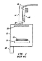
- Figure 1 is a schematic diagram showing a plasma processing environment according to the prior art in which the plasma is remotely generated in an applicator.
- the plasma processing environment includes a process chamber 12 and an applicator 14 for remotely generating a plasma.
- the typical plasma applicator comprises a tube, open at at least one end, through which a reactive gas is pumped.
- the reactive gas is supplied from a source 16 and may comprise such well known process gases as CF 4 , O 2 , N 2 , Cl 2 NF 3 , and methanol.
- a waveguide 18 is provided to direct a source of electromagnetic energy to the tube to ignite and maintain a plasma therein.
- the source of electromagnetic energy may be either an RF signal (typically having a frequency of 13.56 MHz) or it may be (and preferably is) a microwave signal (typically having a frequency of 2.45 GHz).
- the plasma thus generated is directed out of the open end of the tube, through a transport conduit 22 toward the process chamber 12, in which a gas distribution plate 26 may be used to spread neutrals and ions for even distribution therein.
- the neutrals and ions are directed towards a workpiece, typically a semiconductor wafer 28.
- a wafer support 30 is provided that may also be used as a cathode, while the walls of the process chamber may be used as an anode.
- Reactive species such as excited species or ions
- the recombination could be due to a collision between the ions, electrons, or neutrals, or a collision with the wall of the delivery tube.
- the composition of ions is not controllable because different reactive species have different levels of ionization energy.
- the ionization rates of different gases in a gas mixture are therefore determined by the minimum ionization energy of the gases.
- the minimum ionization energy for Cl 2 is approximately 11.5 eV, while that for Ar is 15.8 eV.
- the density of Cl + and Cl 2 + ions is much higher than the density of + Ar ions. Changes in RF power, chamber pressure, or flow ratio do not effectively change the composition of ions.
- US-A-5,233,155 shows an applicator for injecting a plasma of non-reactive ions towards a target in a process chamber, the plasma carrying a superalloy coating for the target.
- EP-A-0,388,800 and US-A-4,859,908 by contrast generate a plasma of reactive ions or powders such as Nitrogen, hydrogen or methane in an applicator located outside a process chamber.
- a focused power source generates a high-density plasma spot within the plasma torch.
- the focused power source is an inductively coupled RF coil that partially or completely surrounds the housing.
- the high-density plasma is focused directly into the process chamber through an outlet defined in the torch.
- the shape and dimensions of the outlet are chosen to provide a desired expansion of gas or a hollow electrode effect to focus the RF power to enhance plasma torch strength.
- a plasma torch will be used as an additional plasma source to adjust the composition of ions in the process chamber, I.e., the plasma torch generates a plasma of non-reactive species.
- the plasma is then directly focused into the process chamber to increase the density of the non-reactive ions, to thereby improve the etch process and control the etch profile of a substrate being processed within the process chamber.
- the plasma torch is also used with other plasma sources. The power supplied to the plasma torch and/or the other source could be modulated or pulsed at the same or different frequency for better chemical species composition control.
- the invention provides an apparatus for focusing a plasma torch directly into a process chamber.
- the preferred embodiment of the invention provides an apparatus and method that generates a plasma torch having flow rate ranging from approximately 100 SCCM (Standard Cubic Centimeter per Minute) to 1000 SCCM.
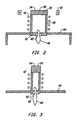
- Figure 2 is a side sectional view of an apparatus 34 for generating a low flow rate plasma torch, in which the applicator for generating a remote plasma includes a housing 36 that is joined to a process chamber 44.
- the applicator is preferably located at the top or side of the process chamber.
- the top 50 and bottom 52 surfaces of the applicator housing may be either flat or hemispherical shaped. The hemispherical shape can help to form a more focused plasma due to hollow electrode effects.
- a process gas is injected into the applicator housing 36 through a narrow channel 38 formed therein.
- the narrow diameter of the channel minimizes the possibility of plasma formation within the channel, as well as the possibility of upstream plasma diffusion.
- a magnet 40 is provided proximate to the channel for generating a magnetic field that enhances the blockage of the plasma to reduce upstream diffusion further.
- the velocity of the gas is controlled by the initial gas. flow rate and by the dimensions of the channel. For example, a flow rate of between 10 cm3 per minute and 100 cm3 per minute is achieved with a channel diameter of about 0.31 cm to 0.05 cm (1/8 in. to 0.2 in) or less, and a channel length of about 0.64 cm (1/4 in.) or longer. The same flow rate may also be achieved by providing a higher initial flow rate through a wider channel.
- the applicator housing has a diameter having a range of from about 0.16 to 2.54 cm (1/16 in. to about 1 in.).
- the length to diameter ratio of the housing is from about 1:1 to about 10:1. See, for example Figure 3, which is a side sectional view of an apparatus 54 for generating a high flow rate plasma torch.
- the housing diameter is from about 2.45 to 7.62 cm (1 in. to about 3 in.), and the length to diameter ratio is from about 1:1 to about 0.1:1.
- the focused power source is an inductively coupled radio frequency (“RF") coil 42 that partially or completely surrounds the applicator housing.
- the coil preferably has between 1 to 10 turns, with a coil spacing of about 1 mm or larger. At a fixed power, more turns result in less RF current through the coil, but higher RF voltage, and higher capacitive coupling from coil to plasma.
- the frequency of the RF signal that is applied to the gas is about 2 MHz or higher, and preferably about 13.56 MHz or higher.
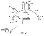
- Figure 4 is a side sectional view of an applicator and process chamber 66, in which the applicator disclosed herein is provided to inject non-reactive ions into the process chamber.
- a non-reactive gas 67 such as He, is pumped into the applicator housing 68.
- the gas is typically of a type as is used for the generation of non-reactive ions and may alternately be an inert gas, such as Ar or Xe, or any gases that can form a passivation layer to protect the side wall of etched features, such as gases that are rich in C and/or Si.
- a power source such as that provided by inductive coupling to the reactive gas via the RF coils 70 when the coils are supplied with RF signal at a constant frequency of 13.56 MHz generates non-reactive He + ions 72 within the applicator with or without power magnitude modulation or pulse.
- the applicator produces a plasma torch of these non-reactive ions that is focused into the process chamber 76.
- a separate source 78 may be provided to inject a reactive species 80, such as Cl + , Cl 2 + , and Cl 2 , into the process chamber without power modulation.
- Inductive RF coils 82 supplied with an RF signal, for example at a constant frequency of 2 MHZ with a power magnitude modulation at a frequency of about 10KHz and 50% duty ratio, surrounding the process chamber, generate a plasma of reactive ions 84, such as Cl + and Cl 2+ ions, and a lot of negative ions Cl therein.
- the reactive ion plasma may be remotely generated.
- the gas flow rate according to this embodiment of the invention is from approximately 15 SCCM to 200 SCCM.
- the process chamber is typically heated to about 80°C, and is maintained at pressures of about 670 mPa-4Pa (5 to 30 millitorr).
- the density of the non-reactive ions in the chamber may be varied by the addition of ions. Because the ion density of pure inert gas is usually higher than that of many reactive gases, total ion density in the chamber plasma can also be increased by non-reactive ion injection. The injection of such non-reactive ions may also provide sufficient energy to enhance the excitation and ionization of reactive gases within the process chamber.
- the invention is useful for controlling the ratio of reactive ions to non-reactive ions to thereby improve etch process performance. For example, by increasing the ratio of non-reactive to reactive ions the reaction between photoresist and reactive ions is minimized, improving etch selectivity to photoresist. Supplying additional non-reactive ions also minimizes side-wall roughness caused by reactive ion attack.
- the non-reactive ion plasma torch may be focused into the process chamber during a specific time period or step of an etch process. For example, more non-reactive ions may be injected into the process chamber during the main etch step. Fewer or no non-reactive ions may be injected into the process chamber during etch residue removal and profile control steps.
- the etch profile of a substrate is thus readily adjusted by changing the non-reactive ion density. Reducing the etch rate of photoresist by introducing more non-reactive ions also improves etch micro-loading.
- FIG 5 is a circuit diagram of a preferred apparatus that may be used to practice the invention.
- An RF generator 54 supplies power to an inductor 56 which is connected in series with a variable capacitor 58.
- the inductive coil may have various configurations, such as the examples shown in Figures 6a-6c.
- the coil may be straight and cylindrical in shape ( Figures 6a and 6b), where the power is applied at the bottom of the coil 60, or at the top of the coil 62, or the coil may be a curved, funnel shaped coil 64 ( Figure 6c).
- Other focused power sources may also be used to generate the homogeneous plasma.
- capacitively coupled power or microwave power may be applied to the reactive gas inside the process chamber itself.
- the homogeneous plasma is focused directly into the process chamber through an outlet 46 formed in the applicator housing.
- the outlet is preferably hemispherical or cylindrical in shape. Such shapes can provide a desired expansion of gas or a hollow electrode effect to focus the RF power, such that the plasma torch 48 strength is thereby enhanced.
- the diameter of the outlet preferably ranges from about 0.05 to 2.54 cm (0.02 in. to about 1 in.).
- the upper limit of the outlet diameter is determined by the diffusion velocity of the particular gas species, where the gas flow velocity at the outlet is equal to or larger than the diffusion velocity. Contamination of the apparatus by upstream diffusion is thereby minimized.
- the height of the outlet may range from about 0.05 to 5.08 cm (0.02 in. to about 2 in.) to provide optimal plasma focus.
- the applicator housing and outlet are combined A high plasma torch flow rate is thereby achieved. It will be readily apparent to one skilled in the art that the outlet dimensions may be varied to provide other desired plasma torch characteristics.
- the plasma torch may be formed such that the focused plasma is injected partially or entirely within the process chamber. Losses of ions and reactive species may thereby be minimized. It is difficult to generate a plasma of certain species in a larger process chamber. However, because the apparatus generates a very high density of ions and radicals within the confines of the applicator housing, the invention facilitates the generation of a plasma comprising such species.
- the ions in a plasma reactor may be classified as reactive ions and non-reactive ions.
- the reactive ions are those that can react with and remove substrate materials. Examples of such reactive ions are the Cl + and Cl 2 + ions used during a metal etch process.
- Non-reactive ions are those which do not directly react with substrate material. These non-reactive ions, such as Ar + and C + ions may enhance the reaction in the direction of bombardment.
- the efficiency of the etch process and the etch profile of the substrate is responsive to the density and ratio of species within the process chamber. However, the generation of reactive and non-reactive ions is not well controllable in a prior art plasma etch chamber. The desired density of a particular species, and/or the ratio of different species, cannot be easily obtained by changes in RF power, pressure, or flow ratio.
- the plasma torch generates a homogeneous plasma of non-reactive species.
- the plasma is directly focused into the process chamber to increase the density of the non-reactive ions to control etch profile of a substrate in the chamber.
- an endpoint detector 100 as shown in Figure 4 is provided to control with a controller 101 the progression of the etch process.
- a plasma torch of non-reactive ions is selectively focused into the chamber in response to the progression of the process, as detected by endpoint detector.
- more than one applicator may be coupled to a process chamber, such that multiple plasmas are injected into the process chamber.
- Each applicator may provide a plasma torch of the same species or different species.
- these multiple plasma torches may include reactive and non-reactive ions.
- one applicator may provide a mixed-gas plasma for an etch process, while another applicator may provide a non-reactive plasma torch to control the density of the non-reactive ions.
- the plasma torch may also be used in connection with other, conventional plasma generating means, such as conventional remote plasma generation, or plasma generation within the process chamber.
- the power of the plasma torch may be varied by the geometry and placement of the inductive coil. For example, a lower placement around the applicator housing generates a lower power plasma.
- the configuration of a gas distribution plate within the chamber also affects the power and placement of the plasma torch. The plate must be positioned to minimize plasma backflow, and can also be positioned to focus and direct the plasma torch.
Landscapes
- Physics & Mathematics (AREA)
- Engineering & Computer Science (AREA)
- Plasma & Fusion (AREA)
- Electromagnetism (AREA)
- Spectroscopy & Molecular Physics (AREA)
- Chemical & Material Sciences (AREA)
- Analytical Chemistry (AREA)
- Drying Of Semiconductors (AREA)
- Plasma Technology (AREA)
Claims (19)
- Dispositif pour commander le rapport d'ions réactifs et d'ions non réactifs dans une chambre (66) de traitement, la chambre (66) de traitement étant agencée pour contenir un premier plasma d'ions réactifs (84), le dispositif comprenant :une source (70) d'énergie focalisée servant à générer un deuxième plasma homogène d'ions non réactifs (67) dans un applicateur (68) ; etune sortie (46) définie dans ledit applicateur, placée à l'intérieur de ladite chambre (66) de traitement pour focaliser au moins une partie dudit deuxième plasma d'ions non réactifs (67) directement dans ladite chambre (66) de traitement de façon à augmenter une densité des ions non réactifs (67) par rapport à une densité des ions réactifs (84) du premier plasma.
- Dispositif selon la revendication 1, dans lequel l'applicateur (68) comporte un canal étroit formé à travers celui-ci destiné à recevoir ledit flux de gaz.
- Dispositif selon la revendication 1 ou la revendication 2, dans lequel ladite source (70) d'énergie focalisée est un bobinage haute fréquence couplé de manière inductive entourant au moins une partie dudit applicateur.
- Dispositif selon la revendication 3, dans lequel, lors de l'utilisation dudit dispositif, l'énergie délivrée audit bobinage est modulée d'environ 100 Hz à environ 100 KHz.
- Dispositif selon l'une quelconque des revendications 1 à 4, dans lequel ladite source (70) d'énergie focalisée est choisie à partir d'un groupe constitué d'une source couplée de manière capacitive et d'une source hyperfréquence.
- Dispositif selon la revendication 5, dans lequel ladite source d'énergie est modulée.
- Dispositif selon la revendication 5, dans lequel ladite source d'énergie n'est pas modulée.
- Dispositif selon l'une quelconque des revendications 1 à 7, dans lequel ledit applicateur (68), lorsqu'il est utilisé, produit une torche à plasma de faible débit et a un diamètre d'environ 1,6 à 25,4 mm (1/16 pouce à environ 1 pouce), et un rapport de longueur - diamètre d'environ 1 : 1 à environ 10 : 1.
- Dispositif selon l'une quelconque des revendications 1 à 7, dans lequel ledit applicateur (68), lorsqu'il est utilisé, produit une torche à plasma de faible débit et a un diamètre d'environ 25,4 à 75,2 mm (1 pouce à environ 3 pouces), et un rapport longueur - diamètre d'environ 0,1 : 1 à environ 1 : 1.
- Dispositif selon l'une quelconque des revendications 1 à 9, dans lequel ledit applicateur (68) comporte des surfaces supérieure et inférieure, et dans lequel lesdites surfaces sont de forme soit plate soit hémisphérique.
- Dispositif selon la revendication 3, dans lequel ledit bobinage couplé de manière inductive de ladite source (42) d'énergie focalisée entoure complètement ledit applicateur (68).
- Dispositif selon la revendication 3, dans lequel ledit bobinage couplé de manière inductive a une fréquence radio d'environ 2 MHz, ou plus.
- Dispositif selon l'une quelconque des revendications précédentes, comprenant en outre :un système (100, 101) de détecteur de point limite servant à surveiller et à commander la progression de traitement dans ladite chambre (66) de traitement.
- Dispositif selon l'une quelconque des revendications précédentes, dans lequel, en utilisation, le débit des ions non réactifs est d'environ 15 SCCM à environ 200 SCCM.
- Dispositif selon l'une quelconque des revendications précédentes, comprenant en outre :au moins un second applicateur (78) destiné à injecter ledit premier plasma directement dans ladite chambre (66) de traitement.
- Dispositif selon l'une quelconque des revendications précédentes, ladite sortie comprenant en outre :un aimant (40) servant à diminuer la diffusion en amont.
- Traitement de commande du rapport d'ions réactifs et d'ions non réactifs dans une chambre (66) de traitement, comprenant les étapes, dans lesquelles :on forme un premier plasma d'ions réactifs (84) ;on place ledit premier plasma d'ions réactifs dans la chambre (66) de traitement ;on génère un deuxième plasma d'ions non réactifs dans un applicateur (68) via une source (70) d'énergie focalisée ; eton injecte au moins une partie du deuxième plasma dans la chambre de traitement par une sortie définie dans l'applicateur de façon à augmenter une densité des ions non réactifs (67) par rapport à une densité des ions réactifs (84) du premier plasma.
- Traitement selon la revendication 17, comprenant en outre les étapes, dans lesquelles :on utilise un système de détecteur de point limite pour surveiller et commander la progression de traitement dans la chambre (66) de traitement ; eton injecte ledit deuxième plasma dans ladite chambre de traitement en réponse à un signal produit par ledit système de détecteur de point limite.
- Traitement selon la revendication 17, comprenant en outre l'étape d'injection d'au moins une partie d'un troisième plasma directement dans ladite chambre (66) de traitement.
Applications Claiming Priority (2)
| Application Number | Priority Date | Filing Date | Title |
|---|---|---|---|
| US08/761,024 US6312554B1 (en) | 1996-12-05 | 1996-12-05 | Apparatus and method for controlling the ratio of reactive to non-reactive ions in a semiconductor wafer processing chamber |
| US761024 | 1996-12-05 |
Publications (2)
| Publication Number | Publication Date |
|---|---|
| EP0847231A1 EP0847231A1 (fr) | 1998-06-10 |
| EP0847231B1 true EP0847231B1 (fr) | 2003-03-19 |
Family
ID=25060882
Family Applications (1)
| Application Number | Title | Priority Date | Filing Date |
|---|---|---|---|
| EP97309774A Expired - Lifetime EP0847231B1 (fr) | 1996-12-05 | 1997-12-04 | Dispositif et procédé pour la réalisation d'une torche à plasma |
Country Status (6)
| Country | Link |
|---|---|
| US (1) | US6312554B1 (fr) |
| EP (1) | EP0847231B1 (fr) |
| JP (1) | JPH10228997A (fr) |
| KR (1) | KR19980063764A (fr) |
| DE (1) | DE69719925T2 (fr) |
| TW (1) | TW386237B (fr) |
Families Citing this family (153)
| Publication number | Priority date | Publication date | Assignee | Title |
|---|---|---|---|---|
| US7510664B2 (en) * | 2001-01-30 | 2009-03-31 | Rapt Industries, Inc. | Apparatus and method for atmospheric pressure reactive atom plasma processing for shaping of damage free surfaces |
| US7591957B2 (en) | 2001-01-30 | 2009-09-22 | Rapt Industries, Inc. | Method for atmospheric pressure reactive atom plasma processing for surface modification |
| CN1283131C (zh) * | 2001-10-05 | 2006-11-01 | 泰克纳等离子系统公司 | 用于固态电源的多线圈感应等离子体火炬 |
| US6660177B2 (en) | 2001-11-07 | 2003-12-09 | Rapt Industries Inc. | Apparatus and method for reactive atom plasma processing for material deposition |
| JP2006054206A (ja) * | 2002-07-30 | 2006-02-23 | Tokyo Electron Ltd | プラズマ処理装置およびプラズマ処理方法 |
| US20110104381A1 (en) * | 2004-01-15 | 2011-05-05 | Stefan Laure | Plasma Treatment of Large-Scale Components |
| WO2005099320A2 (fr) * | 2004-04-09 | 2005-10-20 | Plasmatreat Gmbh | Procede et dispositif de production d'un plasma basse pression, et applications de ce plasma basse pression |
| JP4570659B2 (ja) * | 2004-08-04 | 2010-10-27 | インダストリー−ユニヴァーシティ コオペレーション ファウンデーション ハニャン ユニヴァーシティ | Dcバイアスを利用したリモートプラズマ原子層蒸着装置及び方法 |
| EP1630849B1 (fr) * | 2004-08-27 | 2011-11-02 | Fei Company | Traitement localisé par plasma |
| WO2006099190A2 (fr) * | 2005-03-11 | 2006-09-21 | Perkinelmer, Inc. | Plasmas et procedes d'utilisation |
| CN101156504B (zh) * | 2005-04-11 | 2012-07-18 | 洛尔等离子技术有限公司 | 等离子喷涂设备及方法 |
| KR100725105B1 (ko) * | 2006-07-12 | 2007-06-04 | 삼성전자주식회사 | 반도체 제조설비의 애플리케이터 |
| TWI318417B (en) | 2006-11-03 | 2009-12-11 | Ind Tech Res Inst | Hollow-type cathode electricity discharging apparatus |
| WO2008104160A2 (fr) * | 2007-02-26 | 2008-09-04 | Dr. Laure Plasmatechnologie Gmbh | Dispositif et procédé pour l'application de revêtement et le traitement de surface assistés par plasma de pièces volumineuses |
| TWI424796B (zh) * | 2010-02-12 | 2014-01-21 | Advanced Micro Fab Equip Inc | Plasma processing device with diffusion dissociation region |
| US8496756B2 (en) | 2010-04-30 | 2013-07-30 | Applied Materials, Inc. | Methods for processing substrates in process systems having shared resources |
| US9324576B2 (en) | 2010-05-27 | 2016-04-26 | Applied Materials, Inc. | Selective etch for silicon films |
| US10283321B2 (en) | 2011-01-18 | 2019-05-07 | Applied Materials, Inc. | Semiconductor processing system and methods using capacitively coupled plasma |
| US8999856B2 (en) | 2011-03-14 | 2015-04-07 | Applied Materials, Inc. | Methods for etch of sin films |
| US9064815B2 (en) | 2011-03-14 | 2015-06-23 | Applied Materials, Inc. | Methods for etch of metal and metal-oxide films |
| US8808563B2 (en) | 2011-10-07 | 2014-08-19 | Applied Materials, Inc. | Selective etch of silicon by way of metastable hydrogen termination |
| CN103094038B (zh) * | 2011-10-27 | 2017-01-11 | 松下知识产权经营株式会社 | 等离子体处理装置以及等离子体处理方法 |
| JP5510437B2 (ja) * | 2011-12-07 | 2014-06-04 | パナソニック株式会社 | プラズマ処理装置及びプラズマ処理方法 |
| US10115565B2 (en) * | 2012-03-02 | 2018-10-30 | Panasonic Intellectual Property Management Co., Ltd. | Plasma processing apparatus and plasma processing method |
| US20130305988A1 (en) * | 2012-05-18 | 2013-11-21 | Axcelis Technologies, Inc. | Inline Capacitive Ignition of Inductively Coupled Plasma Ion Source |
| US9267739B2 (en) | 2012-07-18 | 2016-02-23 | Applied Materials, Inc. | Pedestal with multi-zone temperature control and multiple purge capabilities |
| US9373517B2 (en) | 2012-08-02 | 2016-06-21 | Applied Materials, Inc. | Semiconductor processing with DC assisted RF power for improved control |
| US9034770B2 (en) | 2012-09-17 | 2015-05-19 | Applied Materials, Inc. | Differential silicon oxide etch |
| US9023734B2 (en) | 2012-09-18 | 2015-05-05 | Applied Materials, Inc. | Radical-component oxide etch |
| US9390937B2 (en) | 2012-09-20 | 2016-07-12 | Applied Materials, Inc. | Silicon-carbon-nitride selective etch |
| US9132436B2 (en) | 2012-09-21 | 2015-09-15 | Applied Materials, Inc. | Chemical control features in wafer process equipment |
| US8969212B2 (en) | 2012-11-20 | 2015-03-03 | Applied Materials, Inc. | Dry-etch selectivity |
| US8980763B2 (en) | 2012-11-30 | 2015-03-17 | Applied Materials, Inc. | Dry-etch for selective tungsten removal |
| US9111877B2 (en) | 2012-12-18 | 2015-08-18 | Applied Materials, Inc. | Non-local plasma oxide etch |
| US8921234B2 (en) | 2012-12-21 | 2014-12-30 | Applied Materials, Inc. | Selective titanium nitride etching |
| US10256079B2 (en) | 2013-02-08 | 2019-04-09 | Applied Materials, Inc. | Semiconductor processing systems having multiple plasma configurations |
| US9362130B2 (en) | 2013-03-01 | 2016-06-07 | Applied Materials, Inc. | Enhanced etching processes using remote plasma sources |
| US9040422B2 (en) | 2013-03-05 | 2015-05-26 | Applied Materials, Inc. | Selective titanium nitride removal |
| US20140271097A1 (en) | 2013-03-15 | 2014-09-18 | Applied Materials, Inc. | Processing systems and methods for halide scavenging |
| US9493879B2 (en) | 2013-07-12 | 2016-11-15 | Applied Materials, Inc. | Selective sputtering for pattern transfer |
| JP6037292B2 (ja) * | 2013-08-20 | 2016-12-07 | パナソニックIpマネジメント株式会社 | プラズマ処理装置及びプラズマ処理方法 |
| US9773648B2 (en) | 2013-08-30 | 2017-09-26 | Applied Materials, Inc. | Dual discharge modes operation for remote plasma |
| US9576809B2 (en) | 2013-11-04 | 2017-02-21 | Applied Materials, Inc. | Etch suppression with germanium |
| US9520303B2 (en) | 2013-11-12 | 2016-12-13 | Applied Materials, Inc. | Aluminum selective etch |
| US9245762B2 (en) | 2013-12-02 | 2016-01-26 | Applied Materials, Inc. | Procedure for etch rate consistency |
| WO2015094596A1 (fr) * | 2013-12-17 | 2015-06-25 | Applied Materials, Inc. | Ensembles de systèmes à semi-conducteur et procédés de fonctionnement |
| US9287095B2 (en) | 2013-12-17 | 2016-03-15 | Applied Materials, Inc. | Semiconductor system assemblies and methods of operation |
| US9287134B2 (en) | 2014-01-17 | 2016-03-15 | Applied Materials, Inc. | Titanium oxide etch |
| US9396989B2 (en) | 2014-01-27 | 2016-07-19 | Applied Materials, Inc. | Air gaps between copper lines |
| US9293568B2 (en) | 2014-01-27 | 2016-03-22 | Applied Materials, Inc. | Method of fin patterning |
| US9385028B2 (en) | 2014-02-03 | 2016-07-05 | Applied Materials, Inc. | Air gap process |
| US9499898B2 (en) | 2014-03-03 | 2016-11-22 | Applied Materials, Inc. | Layered thin film heater and method of fabrication |
| US9299575B2 (en) | 2014-03-17 | 2016-03-29 | Applied Materials, Inc. | Gas-phase tungsten etch |
| US9299537B2 (en) | 2014-03-20 | 2016-03-29 | Applied Materials, Inc. | Radial waveguide systems and methods for post-match control of microwaves |
| US9299538B2 (en) | 2014-03-20 | 2016-03-29 | Applied Materials, Inc. | Radial waveguide systems and methods for post-match control of microwaves |
| US9903020B2 (en) | 2014-03-31 | 2018-02-27 | Applied Materials, Inc. | Generation of compact alumina passivation layers on aluminum plasma equipment components |
| US9269590B2 (en) | 2014-04-07 | 2016-02-23 | Applied Materials, Inc. | Spacer formation |
| US9309598B2 (en) | 2014-05-28 | 2016-04-12 | Applied Materials, Inc. | Oxide and metal removal |
| US9406523B2 (en) | 2014-06-19 | 2016-08-02 | Applied Materials, Inc. | Highly selective doped oxide removal method |
| US9378969B2 (en) | 2014-06-19 | 2016-06-28 | Applied Materials, Inc. | Low temperature gas-phase carbon removal |
| US9425058B2 (en) | 2014-07-24 | 2016-08-23 | Applied Materials, Inc. | Simplified litho-etch-litho-etch process |
| US9378978B2 (en) | 2014-07-31 | 2016-06-28 | Applied Materials, Inc. | Integrated oxide recess and floating gate fin trimming |
| US9496167B2 (en) | 2014-07-31 | 2016-11-15 | Applied Materials, Inc. | Integrated bit-line airgap formation and gate stack post clean |
| US9659753B2 (en) | 2014-08-07 | 2017-05-23 | Applied Materials, Inc. | Grooved insulator to reduce leakage current |
| US9553102B2 (en) | 2014-08-19 | 2017-01-24 | Applied Materials, Inc. | Tungsten separation |
| US9355856B2 (en) | 2014-09-12 | 2016-05-31 | Applied Materials, Inc. | V trench dry etch |
| US9478434B2 (en) | 2014-09-24 | 2016-10-25 | Applied Materials, Inc. | Chlorine-based hardmask removal |
| US9368364B2 (en) | 2014-09-24 | 2016-06-14 | Applied Materials, Inc. | Silicon etch process with tunable selectivity to SiO2 and other materials |
| US9613822B2 (en) | 2014-09-25 | 2017-04-04 | Applied Materials, Inc. | Oxide etch selectivity enhancement |
| WO2016051465A1 (fr) * | 2014-09-29 | 2016-04-07 | 株式会社日立国際電気 | Dispositif plasma couplé de manière inductive à pression atmosphérique |
| US9966240B2 (en) | 2014-10-14 | 2018-05-08 | Applied Materials, Inc. | Systems and methods for internal surface conditioning assessment in plasma processing equipment |
| US9355922B2 (en) | 2014-10-14 | 2016-05-31 | Applied Materials, Inc. | Systems and methods for internal surface conditioning in plasma processing equipment |
| US11637002B2 (en) | 2014-11-26 | 2023-04-25 | Applied Materials, Inc. | Methods and systems to enhance process uniformity |
| US9299583B1 (en) | 2014-12-05 | 2016-03-29 | Applied Materials, Inc. | Aluminum oxide selective etch |
| US10224210B2 (en) | 2014-12-09 | 2019-03-05 | Applied Materials, Inc. | Plasma processing system with direct outlet toroidal plasma source |
| US10573496B2 (en) | 2014-12-09 | 2020-02-25 | Applied Materials, Inc. | Direct outlet toroidal plasma source |
| US9502258B2 (en) | 2014-12-23 | 2016-11-22 | Applied Materials, Inc. | Anisotropic gap etch |
| US9343272B1 (en) | 2015-01-08 | 2016-05-17 | Applied Materials, Inc. | Self-aligned process |
| US11257693B2 (en) | 2015-01-09 | 2022-02-22 | Applied Materials, Inc. | Methods and systems to improve pedestal temperature control |
| US9373522B1 (en) | 2015-01-22 | 2016-06-21 | Applied Mateials, Inc. | Titanium nitride removal |
| US9449846B2 (en) | 2015-01-28 | 2016-09-20 | Applied Materials, Inc. | Vertical gate separation |
| US20160225652A1 (en) | 2015-02-03 | 2016-08-04 | Applied Materials, Inc. | Low temperature chuck for plasma processing systems |
| US9728437B2 (en) | 2015-02-03 | 2017-08-08 | Applied Materials, Inc. | High temperature chuck for plasma processing systems |
| US9881805B2 (en) | 2015-03-02 | 2018-01-30 | Applied Materials, Inc. | Silicon selective removal |
| US9741593B2 (en) | 2015-08-06 | 2017-08-22 | Applied Materials, Inc. | Thermal management systems and methods for wafer processing systems |
| US9691645B2 (en) | 2015-08-06 | 2017-06-27 | Applied Materials, Inc. | Bolted wafer chuck thermal management systems and methods for wafer processing systems |
| US9349605B1 (en) | 2015-08-07 | 2016-05-24 | Applied Materials, Inc. | Oxide etch selectivity systems and methods |
| US10504700B2 (en) | 2015-08-27 | 2019-12-10 | Applied Materials, Inc. | Plasma etching systems and methods with secondary plasma injection |
| US10504754B2 (en) | 2016-05-19 | 2019-12-10 | Applied Materials, Inc. | Systems and methods for improved semiconductor etching and component protection |
| US10522371B2 (en) | 2016-05-19 | 2019-12-31 | Applied Materials, Inc. | Systems and methods for improved semiconductor etching and component protection |
| US9865484B1 (en) | 2016-06-29 | 2018-01-09 | Applied Materials, Inc. | Selective etch using material modification and RF pulsing |
| US10062575B2 (en) | 2016-09-09 | 2018-08-28 | Applied Materials, Inc. | Poly directional etch by oxidation |
| US10629473B2 (en) | 2016-09-09 | 2020-04-21 | Applied Materials, Inc. | Footing removal for nitride spacer |
| US10546729B2 (en) | 2016-10-04 | 2020-01-28 | Applied Materials, Inc. | Dual-channel showerhead with improved profile |
| US10062585B2 (en) | 2016-10-04 | 2018-08-28 | Applied Materials, Inc. | Oxygen compatible plasma source |
| US9934942B1 (en) | 2016-10-04 | 2018-04-03 | Applied Materials, Inc. | Chamber with flow-through source |
| US9721789B1 (en) | 2016-10-04 | 2017-08-01 | Applied Materials, Inc. | Saving ion-damaged spacers |
| US10062579B2 (en) | 2016-10-07 | 2018-08-28 | Applied Materials, Inc. | Selective SiN lateral recess |
| US9947549B1 (en) | 2016-10-10 | 2018-04-17 | Applied Materials, Inc. | Cobalt-containing material removal |
| US9768034B1 (en) | 2016-11-11 | 2017-09-19 | Applied Materials, Inc. | Removal methods for high aspect ratio structures |
| US10163696B2 (en) | 2016-11-11 | 2018-12-25 | Applied Materials, Inc. | Selective cobalt removal for bottom up gapfill |
| US10242908B2 (en) | 2016-11-14 | 2019-03-26 | Applied Materials, Inc. | Airgap formation with damage-free copper |
| US10026621B2 (en) | 2016-11-14 | 2018-07-17 | Applied Materials, Inc. | SiN spacer profile patterning |
| US10566206B2 (en) | 2016-12-27 | 2020-02-18 | Applied Materials, Inc. | Systems and methods for anisotropic material breakthrough |
| US10431429B2 (en) | 2017-02-03 | 2019-10-01 | Applied Materials, Inc. | Systems and methods for radial and azimuthal control of plasma uniformity |
| US10403507B2 (en) | 2017-02-03 | 2019-09-03 | Applied Materials, Inc. | Shaped etch profile with oxidation |
| US10043684B1 (en) | 2017-02-06 | 2018-08-07 | Applied Materials, Inc. | Self-limiting atomic thermal etching systems and methods |
| US10319739B2 (en) | 2017-02-08 | 2019-06-11 | Applied Materials, Inc. | Accommodating imperfectly aligned memory holes |
| US10943834B2 (en) | 2017-03-13 | 2021-03-09 | Applied Materials, Inc. | Replacement contact process |
| US10319649B2 (en) | 2017-04-11 | 2019-06-11 | Applied Materials, Inc. | Optical emission spectroscopy (OES) for remote plasma monitoring |
| JP7176860B6 (ja) | 2017-05-17 | 2022-12-16 | アプライド マテリアルズ インコーポレイテッド | 前駆体の流れを改善する半導体処理チャンバ |
| US11276559B2 (en) | 2017-05-17 | 2022-03-15 | Applied Materials, Inc. | Semiconductor processing chamber for multiple precursor flow |
| US11276590B2 (en) | 2017-05-17 | 2022-03-15 | Applied Materials, Inc. | Multi-zone semiconductor substrate supports |
| US10497579B2 (en) | 2017-05-31 | 2019-12-03 | Applied Materials, Inc. | Water-free etching methods |
| US10049891B1 (en) | 2017-05-31 | 2018-08-14 | Applied Materials, Inc. | Selective in situ cobalt residue removal |
| US10920320B2 (en) | 2017-06-16 | 2021-02-16 | Applied Materials, Inc. | Plasma health determination in semiconductor substrate processing reactors |
| US10541246B2 (en) | 2017-06-26 | 2020-01-21 | Applied Materials, Inc. | 3D flash memory cells which discourage cross-cell electrical tunneling |
| US10727080B2 (en) | 2017-07-07 | 2020-07-28 | Applied Materials, Inc. | Tantalum-containing material removal |
| US10541184B2 (en) | 2017-07-11 | 2020-01-21 | Applied Materials, Inc. | Optical emission spectroscopic techniques for monitoring etching |
| US10354889B2 (en) | 2017-07-17 | 2019-07-16 | Applied Materials, Inc. | Non-halogen etching of silicon-containing materials |
| US10170336B1 (en) | 2017-08-04 | 2019-01-01 | Applied Materials, Inc. | Methods for anisotropic control of selective silicon removal |
| US10043674B1 (en) | 2017-08-04 | 2018-08-07 | Applied Materials, Inc. | Germanium etching systems and methods |
| US10297458B2 (en) | 2017-08-07 | 2019-05-21 | Applied Materials, Inc. | Process window widening using coated parts in plasma etch processes |
| US10283324B1 (en) | 2017-10-24 | 2019-05-07 | Applied Materials, Inc. | Oxygen treatment for nitride etching |
| US10128086B1 (en) | 2017-10-24 | 2018-11-13 | Applied Materials, Inc. | Silicon pretreatment for nitride removal |
| US10256112B1 (en) | 2017-12-08 | 2019-04-09 | Applied Materials, Inc. | Selective tungsten removal |
| US10903054B2 (en) | 2017-12-19 | 2021-01-26 | Applied Materials, Inc. | Multi-zone gas distribution systems and methods |
| US11328909B2 (en) | 2017-12-22 | 2022-05-10 | Applied Materials, Inc. | Chamber conditioning and removal processes |
| US10854426B2 (en) | 2018-01-08 | 2020-12-01 | Applied Materials, Inc. | Metal recess for semiconductor structures |
| US10964512B2 (en) | 2018-02-15 | 2021-03-30 | Applied Materials, Inc. | Semiconductor processing chamber multistage mixing apparatus and methods |
| US10679870B2 (en) | 2018-02-15 | 2020-06-09 | Applied Materials, Inc. | Semiconductor processing chamber multistage mixing apparatus |
| TWI766433B (zh) | 2018-02-28 | 2022-06-01 | 美商應用材料股份有限公司 | 形成氣隙的系統及方法 |
| US10593560B2 (en) | 2018-03-01 | 2020-03-17 | Applied Materials, Inc. | Magnetic induction plasma source for semiconductor processes and equipment |
| US10319600B1 (en) | 2018-03-12 | 2019-06-11 | Applied Materials, Inc. | Thermal silicon etch |
| US10497573B2 (en) | 2018-03-13 | 2019-12-03 | Applied Materials, Inc. | Selective atomic layer etching of semiconductor materials |
| US10573527B2 (en) | 2018-04-06 | 2020-02-25 | Applied Materials, Inc. | Gas-phase selective etching systems and methods |
| US10490406B2 (en) | 2018-04-10 | 2019-11-26 | Appled Materials, Inc. | Systems and methods for material breakthrough |
| US10699879B2 (en) | 2018-04-17 | 2020-06-30 | Applied Materials, Inc. | Two piece electrode assembly with gap for plasma control |
| US10886137B2 (en) | 2018-04-30 | 2021-01-05 | Applied Materials, Inc. | Selective nitride removal |
| US10755941B2 (en) | 2018-07-06 | 2020-08-25 | Applied Materials, Inc. | Self-limiting selective etching systems and methods |
| US10872778B2 (en) | 2018-07-06 | 2020-12-22 | Applied Materials, Inc. | Systems and methods utilizing solid-phase etchants |
| US10672642B2 (en) | 2018-07-24 | 2020-06-02 | Applied Materials, Inc. | Systems and methods for pedestal configuration |
| US11049755B2 (en) | 2018-09-14 | 2021-06-29 | Applied Materials, Inc. | Semiconductor substrate supports with embedded RF shield |
| US10892198B2 (en) | 2018-09-14 | 2021-01-12 | Applied Materials, Inc. | Systems and methods for improved performance in semiconductor processing |
| US11062887B2 (en) | 2018-09-17 | 2021-07-13 | Applied Materials, Inc. | High temperature RF heater pedestals |
| US11417534B2 (en) | 2018-09-21 | 2022-08-16 | Applied Materials, Inc. | Selective material removal |
| US11682560B2 (en) | 2018-10-11 | 2023-06-20 | Applied Materials, Inc. | Systems and methods for hafnium-containing film removal |
| US11121002B2 (en) | 2018-10-24 | 2021-09-14 | Applied Materials, Inc. | Systems and methods for etching metals and metal derivatives |
| US11437242B2 (en) | 2018-11-27 | 2022-09-06 | Applied Materials, Inc. | Selective removal of silicon-containing materials |
| US11721527B2 (en) | 2019-01-07 | 2023-08-08 | Applied Materials, Inc. | Processing chamber mixing systems |
| US10920319B2 (en) | 2019-01-11 | 2021-02-16 | Applied Materials, Inc. | Ceramic showerheads with conductive electrodes |
| CN110958773A (zh) * | 2019-12-09 | 2020-04-03 | 福建福顺微电子有限公司 | 一种电路板刻蚀方法 |
| CN113130287B (zh) * | 2020-01-10 | 2025-02-18 | 汉民科技股份有限公司 | 线圈电流分配式的蚀刻机结构 |
Family Cites Families (8)
| Publication number | Priority date | Publication date | Assignee | Title |
|---|---|---|---|---|
| JPH0685206B2 (ja) | 1983-07-12 | 1994-10-26 | ティーディーケイ株式会社 | 磁気記録媒体の製造方法 |
| US4886160A (en) | 1988-11-07 | 1989-12-12 | Kligerman Alan E | Carton for containing a plurality of items for transport, storage and display |
| JPS61222534A (ja) * | 1985-03-28 | 1986-10-03 | Anelva Corp | 表面処理方法および装置 |
| US4859908A (en) | 1986-09-24 | 1989-08-22 | Matsushita Electric Industrial Co., Ltd. | Plasma processing apparatus for large area ion irradiation |
| JP2805009B2 (ja) * | 1988-05-11 | 1998-09-30 | 株式会社日立製作所 | プラズマ発生装置及びプラズマ元素分析装置 |
| US4943345A (en) | 1989-03-23 | 1990-07-24 | Board Of Trustees Operating Michigan State University | Plasma reactor apparatus and method for treating a substrate |
| US5407524A (en) * | 1993-08-13 | 1995-04-18 | Lsi Logic Corporation | End-point detection in plasma etching by monitoring radio frequency matching network |
| JPH09251935A (ja) * | 1996-03-18 | 1997-09-22 | Applied Materials Inc | プラズマ点火装置、プラズマを用いる半導体製造装置及び半導体装置のプラズマ点火方法 |
-
1996
- 1996-12-05 US US08/761,024 patent/US6312554B1/en not_active Expired - Lifetime
-
1997
- 1997-12-04 KR KR1019970065815A patent/KR19980063764A/ko not_active Ceased
- 1997-12-04 TW TW086118257A patent/TW386237B/zh not_active IP Right Cessation
- 1997-12-04 JP JP9366565A patent/JPH10228997A/ja not_active Withdrawn
- 1997-12-04 DE DE69719925T patent/DE69719925T2/de not_active Expired - Fee Related
- 1997-12-04 EP EP97309774A patent/EP0847231B1/fr not_active Expired - Lifetime
Also Published As
| Publication number | Publication date |
|---|---|
| JPH10228997A (ja) | 1998-08-25 |
| DE69719925T2 (de) | 2003-12-11 |
| DE69719925D1 (de) | 2003-04-24 |
| US6312554B1 (en) | 2001-11-06 |
| EP0847231A1 (fr) | 1998-06-10 |
| TW386237B (en) | 2000-04-01 |
| KR19980063764A (ko) | 1998-10-07 |
Similar Documents
| Publication | Publication Date | Title |
|---|---|---|
| EP0847231B1 (fr) | Dispositif et procédé pour la réalisation d'une torche à plasma | |
| Ichiki et al. | Localized and ultrahigh-rate etching of silicon wafers using atmospheric-pressure microplasma jets | |
| TWI536873B (zh) | 低電子溫度微波表面波電漿處理方法及設備 | |
| US5300460A (en) | UHF/VHF plasma for use in forming integrated circuit structures on semiconductor wafers | |
| US5964949A (en) | ICP reactor having a conically-shaped plasma-generating section | |
| EP0379828B1 (fr) | Dispositif de traitement par plasma multipolaire à induction de radiofréquence | |
| US6635578B1 (en) | Method of operating a dual chamber reactor with neutral density decoupled from ion density | |
| US6849857B2 (en) | Beam processing apparatus | |
| US5607542A (en) | Inductively enhanced reactive ion etching | |
| US9301383B2 (en) | Low electron temperature, edge-density enhanced, surface wave plasma (SWP) processing method and apparatus | |
| US20160293386A1 (en) | Energetic negative ion impact ionization plasma | |
| US20100098882A1 (en) | Plasma source for chamber cleaning and process | |
| KR20010040736A (ko) | 종의 밀도를 개별적으로 제어할 수 있는 플라즈마어시스티드 프로세싱 챔버 | |
| EP1529306A1 (fr) | Chambre de gravure a sources de polarisation double frequence et une source de generation de plasma sur une frequence | |
| US6909086B2 (en) | Neutral particle beam processing apparatus | |
| US10790153B2 (en) | Methods and apparatus for electron beam etching process | |
| JPH09185999A (ja) | ラジカルの制御方法 | |
| USH2212H1 (en) | Method and apparatus for producing an ion-ion plasma continuous in time | |
| JP2002503031A (ja) | 種密度を個別制御するプラズマアシスト処理チャンバ | |
| US7060931B2 (en) | Neutral beam source having electromagnet used for etching semiconductor device | |
| Bardos et al. | Superhigh‐rate plasma jet etching of silicon | |
| US6969953B2 (en) | System and method for inductive coupling of an expanding thermal plasma | |
| US6037267A (en) | Method of etching metallic film for semiconductor devices | |
| EP0472941A2 (fr) | Procédé de fabrication de structures de circuit intégré sur des substrats semi-conducteurs utilisant un plasma VHF/UHF | |
| JP3123203B2 (ja) | プラズマ装置および該装置の使用方法 |
Legal Events
| Date | Code | Title | Description |
|---|---|---|---|
| PUAI | Public reference made under article 153(3) epc to a published international application that has entered the european phase |
Free format text: ORIGINAL CODE: 0009012 |
|
| AK | Designated contracting states |
Kind code of ref document: A1 Designated state(s): DE FR GB |
|
| AX | Request for extension of the european patent |
Free format text: AL;LT;LV;MK;RO;SI |
|
| 17P | Request for examination filed |
Effective date: 19981127 |
|
| AKX | Designation fees paid |
Free format text: DE FR GB |
|
| RBV | Designated contracting states (corrected) |
Designated state(s): DE FR GB |
|
| 17Q | First examination report despatched |
Effective date: 20001025 |
|
| GRAG | Despatch of communication of intention to grant |
Free format text: ORIGINAL CODE: EPIDOS AGRA |
|
| GRAG | Despatch of communication of intention to grant |
Free format text: ORIGINAL CODE: EPIDOS AGRA |
|
| GRAH | Despatch of communication of intention to grant a patent |
Free format text: ORIGINAL CODE: EPIDOS IGRA |
|
| GRAH | Despatch of communication of intention to grant a patent |
Free format text: ORIGINAL CODE: EPIDOS IGRA |
|
| GRAA | (expected) grant |
Free format text: ORIGINAL CODE: 0009210 |
|
| AK | Designated contracting states |
Designated state(s): DE FR GB |
|
| REG | Reference to a national code |
Ref country code: GB Ref legal event code: FG4D |
|
| REF | Corresponds to: |
Ref document number: 69719925 Country of ref document: DE Date of ref document: 20030424 Kind code of ref document: P |
|
| ET | Fr: translation filed | ||
| PG25 | Lapsed in a contracting state [announced via postgrant information from national office to epo] |
Ref country code: GB Free format text: LAPSE BECAUSE OF NON-PAYMENT OF DUE FEES Effective date: 20031204 |
|
| PLBE | No opposition filed within time limit |
Free format text: ORIGINAL CODE: 0009261 |
|
| STAA | Information on the status of an ep patent application or granted ep patent |
Free format text: STATUS: NO OPPOSITION FILED WITHIN TIME LIMIT |
|
| 26N | No opposition filed |
Effective date: 20031222 |
|
| PG25 | Lapsed in a contracting state [announced via postgrant information from national office to epo] |
Ref country code: DE Free format text: LAPSE BECAUSE OF NON-PAYMENT OF DUE FEES Effective date: 20040701 |
|
| GBPC | Gb: european patent ceased through non-payment of renewal fee |
Effective date: 20031204 |
|
| PG25 | Lapsed in a contracting state [announced via postgrant information from national office to epo] |
Ref country code: FR Free format text: LAPSE BECAUSE OF NON-PAYMENT OF DUE FEES Effective date: 20040831 |
|
| REG | Reference to a national code |
Ref country code: FR Ref legal event code: ST |