EP0847602B1 - Kontaktblock mit schnappverbindung - Google Patents
Kontaktblock mit schnappverbindung Download PDFInfo
- Publication number
- EP0847602B1 EP0847602B1 EP96929701A EP96929701A EP0847602B1 EP 0847602 B1 EP0847602 B1 EP 0847602B1 EP 96929701 A EP96929701 A EP 96929701A EP 96929701 A EP96929701 A EP 96929701A EP 0847602 B1 EP0847602 B1 EP 0847602B1
- Authority
- EP
- European Patent Office
- Prior art keywords
- battery pack
- contact
- edge
- electrical
- contact block
- Prior art date
- Legal status (The legal status is an assumption and is not a legal conclusion. Google has not performed a legal analysis and makes no representation as to the accuracy of the status listed.)
- Expired - Lifetime
Links
- 239000000463 material Substances 0.000 claims description 4
- 239000004020 conductor Substances 0.000 description 7
- 230000001413 cellular effect Effects 0.000 description 3
- 239000004033 plastic Substances 0.000 description 3
- -1 for example Substances 0.000 description 1
- 238000010348 incorporation Methods 0.000 description 1
- 238000009434 installation Methods 0.000 description 1
- 230000002045 lasting effect Effects 0.000 description 1
- 239000002184 metal Substances 0.000 description 1
- 238000000034 method Methods 0.000 description 1
- 238000012986 modification Methods 0.000 description 1
- 230000004048 modification Effects 0.000 description 1
- 239000002991 molded plastic Substances 0.000 description 1
- 238000006467 substitution reaction Methods 0.000 description 1
- 238000003466 welding Methods 0.000 description 1
Images


Classifications
-
- H—ELECTRICITY
- H01—ELECTRIC ELEMENTS
- H01R—ELECTRICALLY-CONDUCTIVE CONNECTIONS; STRUCTURAL ASSOCIATIONS OF A PLURALITY OF MUTUALLY-INSULATED ELECTRICAL CONNECTING ELEMENTS; COUPLING DEVICES; CURRENT COLLECTORS
- H01R13/00—Details of coupling devices of the kinds covered by groups H01R12/70 or H01R24/00 - H01R33/00
- H01R13/02—Contact members
- H01R13/22—Contacts for co-operating by abutting
-
- H—ELECTRICITY
- H01—ELECTRIC ELEMENTS
- H01M—PROCESSES OR MEANS, e.g. BATTERIES, FOR THE DIRECT CONVERSION OF CHEMICAL ENERGY INTO ELECTRICAL ENERGY
- H01M50/00—Constructional details or processes of manufacture of the non-active parts of electrochemical cells other than fuel cells, e.g. hybrid cells
- H01M50/20—Mountings; Secondary casings or frames; Racks, modules or packs; Suspension devices; Shock absorbers; Transport or carrying devices; Holders
- H01M50/204—Racks, modules or packs for multiple batteries or multiple cells
- H01M50/207—Racks, modules or packs for multiple batteries or multiple cells characterised by their shape
- H01M50/213—Racks, modules or packs for multiple batteries or multiple cells characterised by their shape adapted for cells having curved cross-section, e.g. round or elliptic
-
- H—ELECTRICITY
- H01—ELECTRIC ELEMENTS
- H01R—ELECTRICALLY-CONDUCTIVE CONNECTIONS; STRUCTURAL ASSOCIATIONS OF A PLURALITY OF MUTUALLY-INSULATED ELECTRICAL CONNECTING ELEMENTS; COUPLING DEVICES; CURRENT COLLECTORS
- H01R4/00—Electrically-conductive connections between two or more conductive members in direct contact, i.e. touching one another; Means for effecting or maintaining such contact; Electrically-conductive connections having two or more spaced connecting locations for conductors and using contact members penetrating insulation
- H01R4/58—Electrically-conductive connections between two or more conductive members in direct contact, i.e. touching one another; Means for effecting or maintaining such contact; Electrically-conductive connections having two or more spaced connecting locations for conductors and using contact members penetrating insulation characterised by the form or material of the contacting members
-
- H—ELECTRICITY
- H01—ELECTRIC ELEMENTS
- H01M—PROCESSES OR MEANS, e.g. BATTERIES, FOR THE DIRECT CONVERSION OF CHEMICAL ENERGY INTO ELECTRICAL ENERGY
- H01M50/00—Constructional details or processes of manufacture of the non-active parts of electrochemical cells other than fuel cells, e.g. hybrid cells
- H01M50/50—Current conducting connections for cells or batteries
-
- Y—GENERAL TAGGING OF NEW TECHNOLOGICAL DEVELOPMENTS; GENERAL TAGGING OF CROSS-SECTIONAL TECHNOLOGIES SPANNING OVER SEVERAL SECTIONS OF THE IPC; TECHNICAL SUBJECTS COVERED BY FORMER USPC CROSS-REFERENCE ART COLLECTIONS [XRACs] AND DIGESTS
- Y02—TECHNOLOGIES OR APPLICATIONS FOR MITIGATION OR ADAPTATION AGAINST CLIMATE CHANGE
- Y02E—REDUCTION OF GREENHOUSE GAS [GHG] EMISSIONS, RELATED TO ENERGY GENERATION, TRANSMISSION OR DISTRIBUTION
- Y02E60/00—Enabling technologies; Technologies with a potential or indirect contribution to GHG emissions mitigation
- Y02E60/10—Energy storage using batteries
Definitions
- This invention relates in general to connectors for electrical devices, and more particularly to contact blocks for supporting electrical contacts used for electrically interconnecting electrical devices.
- the typical surface contact is a flat conductor mechanically supported by an electrically insulative material such as plastic.
- an electrically insulative material such as plastic.
- One common way of providing alignment of contacts between two devices is to employ a connector or contact block.
- the contacts are embedded in a block of, for example, plastic, leaving the contact surface exposed on a portion of the block.
- the contact block has a body 12 which is fabricated from an electrically insulative material such as, for example, plastic. At least one electrical contact 14 is disposed in the body 12, and has a first contact surface 16 and a second contact surface 18.
- the electrical contact is fabricated from an electrically conductive material, and is preferably a metal insert molded into the body 12. In many cases, at least two electrical contacts will be required, and when two or more are present, they are preferably recessed slightly into the body 12 so that ridges 15 separate the electrical contacts. The purpose of recessing the electrical contacts is to reduce the risk of shorting the contacts together, such as by a coin or keys.
- Top 20 and front 24 define a first edge 32, which has a first ledge 34 formed along the length of the first edge. It is contemplated that the first ledge need not be formed along the entire length of the first edge, but should be formed along at least a portion of the first edge.
- a second edge 36 is defined where bottom 22 and back 26 meet, and a second ledge 38 is formed along second edge 36.
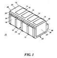
- Contact block 10 is shown connected to an electrical circuit 50, which in the case of a battery pack, includes at least one battery cell 52.
- the circuit components 54 may be carried on a flexible circuit board 56.
- the circuit board 56 may be a more typical rigid board, but it is preferred that the connection between the board and contact block be a flexible carrier, the carrier being connected to the first contact surface(s) shown in FIG. 1. This will facilitate assembly.
- the circuit portion comprising contact block 10, electrical circuit 50, and battery cell(s) 52, is placed into housing 42.
- the contact block is snapped into place in opening 44 by engaging the front 24 of the contact block with the first edge of the opening, and the bottom 22 of the contact block with second edge of the opening.
- a small amount of force applied to the contact block is transmitted to the edges of the opening, causing them to deflect slightly, until first ledge 34 and second ledge 38 become engaged with first edge 46 and second edge 48, respectively.
- contact surface 18 is accessible through opening 44. By snapping the contact block into place, it is held throughout the assembly process.
- the battery pack 40 can be manipulated without moving the contact block out of it's position. In practice this significantly improves assembly time of an electrical device, such as battery pack 40.
- cover 58 is attached to housing 42 by, for example, ultrasonic welding. The final position of the cover is such that it locks the contact block in place, and thereby prevents unintentional disengagement of the contact block from the housing.
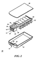
- FIG 3 shows the final assembly in more detail.
- FIG. 3 where there is illustrated therein a side cutaway view of contact block 10 assembled into housing 42. From this view the engagement of first ledge 34 and second ledge 38 of the contact block with first edge 46 and second edge 48 of the opening of the housing can be seen.
- the first contact surface 16 is connected to circuit board or carrier 56, thereby allowing an electrical interconnection through exposed contact surface 18 with a second electrical device 60 when moved in the direction of arrow 62.
- the second electrical device could be, for example, a charger.
- a third electrical device 64 may be simultaneously connected by contacting contact surface 66 of the third electrical device with a third contact surface 68 of contact 14 on the bottom 22 of the contact block 10.
- FIG. 4 illustrates an alternate preferred embodiment of contact block 10.
- electrical contact 14 is configured such that a tab of the conducting material extends from the back 26 of the body 12. This leaves the first contact surface 16 exposed at a position behind the body instead of on the top 20. This provides a location for connecting to a circuit board, as in FIG. 2. However, the back surface of the body acts as a guide to align the circuit board during assembly.
Landscapes
- Chemical & Material Sciences (AREA)
- Chemical Kinetics & Catalysis (AREA)
- Electrochemistry (AREA)
- General Chemical & Material Sciences (AREA)
- Battery Mounting, Suspending (AREA)
Claims (10)
- Batteriepack (40), umfassend:ein Gehäuse (42), welches aus einem elektrisch isolierenden Material hergestellt ist und eine darin ausgebildete Öffnung (44) aufweist, wobei die Öffnung eine erste und eine zweite Kante (46, 48) aufweist;eine elektrische Schaltung (50), welche wenigstens eine in dem Gehäuse angeordnete Batteriezelle (52) umfasst;einen Kontaktblock (10), um die elektrische Schaltung an eine elektrische Vorrichtung (64) anzuschließen, wobei der Kontaktblock einen aus einem elektrisch isolierenden Material hergestellten Körper (12) aufweist und vorspringende Kanten (34, 38) aufweist, um die erste und die zweite Kante der Öffnung in dem Gehäuse unter Verbiegen in Eingriff zu nehmen; sowieeinen Deckel (58), um den Batteriepack abzudecken und den Kontaktblock zu befestigen.
- Batteriepack (40) nach Anspruch 1, wobei der Körper (12) des Kontaktblocks (10) eine Oberseite (20), eine Unterseite (22), eine Vorderseite (24), eine Rückseite (26) und zwei entgegengesetzte Seiten (27, 28) aufweist, wobei die Oberseite entlang der Vorderseite eine erste Kante (32) definiert, wobei die Unterseite entlang der Rückseite eine zweite Kante (36) definiert und wobei der Kontaktblock umfasst:wobei die erste vorspringende Kante (34) entlang wenigstens eines Abschnitts der ersten Kante (32) des Körpers ausgebildet ist, um die erste Kante (46) der Öffnung (44) in dem Gehäuse (42) unter Verbiegen in Eingriff zu nehmen; undwenigstens einen elektrischen Kontakt (14), welcher in dem Körper des Kontaktblocks angeordnet ist und welcher eine erste Kontaktfläche (16) aufweist, um die elektrische Schaltung (50) der ersten elektrischen Vorrichtung elektrisch zu kontaktieren, sowie eine zweite Kontaktfläche (18) aufweist, um eine zweite elektrische Vorrichtung elektrisch zu kontaktieren;
wobei die zweite vorspringende Kante (38) entlang wenigstens eines Abschnitts der zweiten Kante (36) des Körpers ausgebildet ist, um die zweite Kante (48) der in dem Gehäuse ausgebildeten Öffnung unter Verbiegen in Eingriff zu nehmen. - Batteriepack (40) nach Anspruch 2, wobei der wenigstens eine elektrische Kontakt (14) ferner eine dritte Kontaktfläche (30) umfasst, welche an der Unterseite (22) des Körpers angeordnet ist, um die erste elektrische Vorrichtung an eine dritte elektrische Vorrichtung elektrisch anzuschließen.
- Batteriepack (40) nach Anspruch 2, wobei der wenigstens eine elektrische Kontakt (14) wenigstens zwei elektrische Kontakte (14, 16, 18) ist.
- Batteriepack (40) nach Anspruch 4, wobei die wenigstens zwei Kontakte (14, 16, 18) in den Körper (12) eingelassen sind.
- Batteriepack (40) nach Anspruch 2, wobei die erste vorspringende Kante (34) entlang der gesamten ersten Kante (32) des Körpers (12) verläuft.
- Batteriepack (40) nach Anspruch 2, wobei die zweite vorspringende Kante (38) entlang der gesamten zweiten Kante (36) des Körpers (12) verläuft.
- Batteriepack (40) nach Anspruch 2, wobei die erste Kontaktfläche (16) des wenigstens einen elektrischen Kontaktes auf der Oberseite des Körpers (12) angeordnet ist.
- Batteriepack (40) nach Anspruch 2, wobei sich die erste Kontaktfläche (16) von der Rückseite (26) des Körpers (12) erstreckt.
- Batteriepack (40) nach Anspruch 1, wobei der Kontaktblock (10) sowohl eine hörbare als auch eine fühlbare Rückkopplung erzeugt, wenn er in das Gehäuse (42) eingebaut wird.
Applications Claiming Priority (3)
| Application Number | Priority Date | Filing Date | Title |
|---|---|---|---|
| US520359 | 1983-08-04 | ||
| US08/520,359 US5626980A (en) | 1995-08-28 | 1995-08-28 | Contact block in a battery pack having snap in features |
| PCT/US1996/013442 WO1997008777A1 (en) | 1995-08-28 | 1996-08-20 | Contact block having snap in features |
Publications (3)
| Publication Number | Publication Date |
|---|---|
| EP0847602A1 EP0847602A1 (de) | 1998-06-17 |
| EP0847602A4 EP0847602A4 (de) | 1998-11-18 |
| EP0847602B1 true EP0847602B1 (de) | 2002-04-24 |
Family
ID=24072262
Family Applications (1)
| Application Number | Title | Priority Date | Filing Date |
|---|---|---|---|
| EP96929701A Expired - Lifetime EP0847602B1 (de) | 1995-08-28 | 1996-08-20 | Kontaktblock mit schnappverbindung |
Country Status (8)
| Country | Link |
|---|---|
| US (1) | US5626980A (de) |
| EP (1) | EP0847602B1 (de) |
| JP (1) | JP3294279B2 (de) |
| KR (1) | KR100311700B1 (de) |
| CN (1) | CN1096721C (de) |
| CA (1) | CA2229817C (de) |
| DE (1) | DE69620893T2 (de) |
| WO (1) | WO1997008777A1 (de) |
Families Citing this family (8)
| Publication number | Priority date | Publication date | Assignee | Title |
|---|---|---|---|---|
| US5850078A (en) * | 1996-01-16 | 1998-12-15 | Symbol Technologies, Inc. | Simplified assembly and automatic testing of components in electro-optical systems for reading coded indicia |
| US5786106A (en) * | 1996-06-24 | 1998-07-28 | Armani; Shane | Battery pack with interchangeable tag-along supplemental feature cartridge particularly for cellular telephones |
| US5770330A (en) * | 1996-10-24 | 1998-06-23 | Motorola, Inc. | Battery package with multiple surface charging contacts |
| JP3454748B2 (ja) * | 1999-02-26 | 2003-10-06 | 三洋電機株式会社 | パック電池 |
| US6171138B1 (en) * | 2000-01-28 | 2001-01-09 | Motorola, Inc. | Electrical connector for removable components |
| JP2003324783A (ja) * | 2002-05-02 | 2003-11-14 | Mitsubishi Electric Corp | 差込口の配設構造および携帯装置 |
| KR100468318B1 (ko) * | 2002-11-21 | 2005-01-27 | (주)대호하이텍 | 휴대폰 배터리용 터미널 콘택트 및 터미널 콘택트와스페이서의 결합 구조를 가진 터미널 콘택트 어셈블리의제조 방법 |
| DE102004003217A1 (de) * | 2004-01-22 | 2005-08-11 | Braun Gmbh | Anordnung mit einer Batterie und einem Verbindungselement |
Family Cites Families (9)
| Publication number | Priority date | Publication date | Assignee | Title |
|---|---|---|---|---|
| JPS5766864U (de) * | 1980-10-08 | 1982-04-21 | ||
| US4576430A (en) * | 1984-05-30 | 1986-03-18 | Dufresne Raymond A | Snap cable clamp apparatus for battery terminals |
| US4655524A (en) * | 1985-01-07 | 1987-04-07 | Rogers Corporation | Solderless connection apparatus |
| ES2079562T3 (es) * | 1990-04-02 | 1996-01-16 | Whitaker Corp | Conectadores para montaje en superficie. |
| IT220654Z2 (it) * | 1990-10-30 | 1993-10-08 | Marelli Autronica | Connettore per una unita' di controllo di una funzione di un motore a combustione interna |
| US5180644A (en) * | 1992-03-09 | 1993-01-19 | Motorola, Inc. | Weldless battery pack |
| US5183404A (en) * | 1992-04-08 | 1993-02-02 | Megahertz Corporation | Systems for connection of physical/electrical media connectors to computer communications cards |
| US5415570A (en) * | 1992-12-28 | 1995-05-16 | At&T Corp. | Modular connector with contacts associated with more than one surface |
| US5421745A (en) * | 1994-01-03 | 1995-06-06 | Motorola, Inc. | Contact array |
-
1995
- 1995-08-28 US US08/520,359 patent/US5626980A/en not_active Expired - Fee Related
-
1996
- 1996-08-20 JP JP51038097A patent/JP3294279B2/ja not_active Expired - Fee Related
- 1996-08-20 KR KR1019980701494A patent/KR100311700B1/ko not_active Expired - Fee Related
- 1996-08-20 CN CN96196596A patent/CN1096721C/zh not_active Expired - Fee Related
- 1996-08-20 DE DE69620893T patent/DE69620893T2/de not_active Expired - Fee Related
- 1996-08-20 CA CA002229817A patent/CA2229817C/en not_active Expired - Fee Related
- 1996-08-20 WO PCT/US1996/013442 patent/WO1997008777A1/en not_active Ceased
- 1996-08-20 EP EP96929701A patent/EP0847602B1/de not_active Expired - Lifetime
Also Published As
| Publication number | Publication date |
|---|---|
| KR19990044258A (ko) | 1999-06-25 |
| CA2229817C (en) | 2001-01-02 |
| KR100311700B1 (ko) | 2001-12-17 |
| EP0847602A4 (de) | 1998-11-18 |
| JPH11512228A (ja) | 1999-10-19 |
| WO1997008777A1 (en) | 1997-03-06 |
| EP0847602A1 (de) | 1998-06-17 |
| CN1096721C (zh) | 2002-12-18 |
| CN1194729A (zh) | 1998-09-30 |
| JP3294279B2 (ja) | 2002-06-24 |
| US5626980A (en) | 1997-05-06 |
| DE69620893T2 (de) | 2002-10-10 |
| DE69620893D1 (de) | 2002-05-29 |
Similar Documents
| Publication | Publication Date | Title |
|---|---|---|
| US11217942B2 (en) | Connector having metal shell with anti-displacement structure | |
| US6648695B1 (en) | Electrical adapter for connecting connectors of different interface | |
| US5164880A (en) | Electrostatic discharge protection device for a printed circuit board | |
| US6695628B2 (en) | Battery connector | |
| US7021969B2 (en) | Connector allowing reduction in thickness of an apparatus to which the connector is to be mounted | |
| EP0107288B1 (de) | Elektrischer Verbinderzusammenbau zum Anschliessen eines elektrischen abgeschirmten Flachkabels | |
| US5518424A (en) | Connector for a battery | |
| EP0746062B1 (de) | Flächenverbindbarer elektrischer Steckverbinder | |
| US4029377A (en) | Push-on bus bar | |
| US6685508B2 (en) | USB connector assembly having reduced mating height | |
| US6663407B1 (en) | Card edge connector having latches | |
| US6554640B1 (en) | Radio communication equipment having a floating connector | |
| EP0847602B1 (de) | Kontaktblock mit schnappverbindung | |
| CN113725668A (zh) | 正反双面电连接器 | |
| US6652302B1 (en) | Electrical connector with pivotable contact | |
| US6699066B2 (en) | Electrical connector assembly | |
| US6224388B1 (en) | In-board connector | |
| US5967806A (en) | Electrical connector arrangement | |
| US6146172A (en) | Electrical connector | |
| US5741154A (en) | Electrical connector for flat cable | |
| US6652311B2 (en) | Polarized connector for flat flexible circuitry | |
| CN112640224A (zh) | C型通用串列汇流排连接器 | |
| EP1681744A1 (de) | Verbinder | |
| JP2004192967A (ja) | Fpc用コネクタおよびこれを用いた携帯電話機 | |
| EP0265201A3 (de) | Umhüllung für einen elektrischen Kabelverbinder |
Legal Events
| Date | Code | Title | Description |
|---|---|---|---|
| PUAI | Public reference made under article 153(3) epc to a published international application that has entered the european phase |
Free format text: ORIGINAL CODE: 0009012 |
|
| 17P | Request for examination filed |
Effective date: 19980330 |
|
| AK | Designated contracting states |
Kind code of ref document: A1 Designated state(s): DE FR GB |
|
| A4 | Supplementary search report drawn up and despatched |
Effective date: 19980929 |
|
| AK | Designated contracting states |
Kind code of ref document: A4 Designated state(s): DE FR GB |
|
| 17Q | First examination report despatched |
Effective date: 20000704 |
|
| GRAG | Despatch of communication of intention to grant |
Free format text: ORIGINAL CODE: EPIDOS AGRA |
|
| GRAG | Despatch of communication of intention to grant |
Free format text: ORIGINAL CODE: EPIDOS AGRA |
|
| GRAH | Despatch of communication of intention to grant a patent |
Free format text: ORIGINAL CODE: EPIDOS IGRA |
|
| REG | Reference to a national code |
Ref country code: GB Ref legal event code: IF02 |
|
| GRAH | Despatch of communication of intention to grant a patent |
Free format text: ORIGINAL CODE: EPIDOS IGRA |
|
| GRAA | (expected) grant |
Free format text: ORIGINAL CODE: 0009210 |
|
| AK | Designated contracting states |
Kind code of ref document: B1 Designated state(s): DE FR GB |
|
| REG | Reference to a national code |
Ref country code: GB Ref legal event code: FG4D |
|
| REF | Corresponds to: |
Ref document number: 69620893 Country of ref document: DE Date of ref document: 20020529 |
|
| ET | Fr: translation filed | ||
| PLBE | No opposition filed within time limit |
Free format text: ORIGINAL CODE: 0009261 |
|
| STAA | Information on the status of an ep patent application or granted ep patent |
Free format text: STATUS: NO OPPOSITION FILED WITHIN TIME LIMIT |
|
| 26N | No opposition filed |
Effective date: 20030127 |
|
| PGFP | Annual fee paid to national office [announced via postgrant information from national office to epo] |
Ref country code: GB Payment date: 20040707 Year of fee payment: 9 |
|
| PGFP | Annual fee paid to national office [announced via postgrant information from national office to epo] |
Ref country code: FR Payment date: 20040804 Year of fee payment: 9 |
|
| PGFP | Annual fee paid to national office [announced via postgrant information from national office to epo] |
Ref country code: DE Payment date: 20040831 Year of fee payment: 9 |
|
| PG25 | Lapsed in a contracting state [announced via postgrant information from national office to epo] |
Ref country code: GB Free format text: LAPSE BECAUSE OF NON-PAYMENT OF DUE FEES Effective date: 20050820 |
|
| PG25 | Lapsed in a contracting state [announced via postgrant information from national office to epo] |
Ref country code: DE Free format text: LAPSE BECAUSE OF NON-PAYMENT OF DUE FEES Effective date: 20060301 |
|
| GBPC | Gb: european patent ceased through non-payment of renewal fee |
Effective date: 20050820 |
|
| PG25 | Lapsed in a contracting state [announced via postgrant information from national office to epo] |
Ref country code: FR Free format text: LAPSE BECAUSE OF NON-PAYMENT OF DUE FEES Effective date: 20060428 |
|
| REG | Reference to a national code |
Ref country code: FR Ref legal event code: ST Effective date: 20060428 |
|
| P01 | Opt-out of the competence of the unified patent court (upc) registered |
Effective date: 20230520 |