EP0847623B1 - Tampon de sortie a noeuds intermediaires partages - Google Patents
Tampon de sortie a noeuds intermediaires partages Download PDFInfo
- Publication number
- EP0847623B1 EP0847623B1 EP96923751A EP96923751A EP0847623B1 EP 0847623 B1 EP0847623 B1 EP 0847623B1 EP 96923751 A EP96923751 A EP 96923751A EP 96923751 A EP96923751 A EP 96923751A EP 0847623 B1 EP0847623 B1 EP 0847623B1
- Authority
- EP
- European Patent Office
- Prior art keywords
- output
- terminal
- power supply
- circuit
- coupled
- Prior art date
- Legal status (The legal status is an assumption and is not a legal conclusion. Google has not performed a legal analysis and makes no representation as to the accuracy of the status listed.)
- Expired - Lifetime
Links
- 239000000872 buffer Substances 0.000 title claims description 134
- 230000007704 transition Effects 0.000 claims description 14
- 230000000295 complement effect Effects 0.000 claims description 9
- 230000003247 decreasing effect Effects 0.000 claims description 6
- 238000010586 diagram Methods 0.000 description 7
- 230000001052 transient effect Effects 0.000 description 7
- 238000013461 design Methods 0.000 description 5
- 230000008901 benefit Effects 0.000 description 4
- 230000007423 decrease Effects 0.000 description 4
- 238000000034 method Methods 0.000 description 3
- 230000006872 improvement Effects 0.000 description 2
- 238000012546 transfer Methods 0.000 description 2
- 238000013459 approach Methods 0.000 description 1
- 230000008878 coupling Effects 0.000 description 1
- 238000010168 coupling process Methods 0.000 description 1
- 238000005859 coupling reaction Methods 0.000 description 1
- 230000001934 delay Effects 0.000 description 1
- 238000002955 isolation Methods 0.000 description 1
- 238000012545 processing Methods 0.000 description 1
- 230000009467 reduction Effects 0.000 description 1
- 239000004065 semiconductor Substances 0.000 description 1
- 238000000926 separation method Methods 0.000 description 1
- 230000011664 signaling Effects 0.000 description 1
- 230000001360 synchronised effect Effects 0.000 description 1
Images


Classifications
-
- H—ELECTRICITY
- H03—ELECTRONIC CIRCUITRY
- H03K—PULSE TECHNIQUE
- H03K19/00—Logic circuits, i.e. having at least two inputs acting on one output; Inverting circuits
-
- H—ELECTRICITY
- H03—ELECTRONIC CIRCUITRY
- H03K—PULSE TECHNIQUE
- H03K19/00—Logic circuits, i.e. having at least two inputs acting on one output; Inverting circuits
- H03K19/003—Modifications for increasing the reliability for protection
- H03K19/00346—Modifications for eliminating interference or parasitic voltages or currents
- H03K19/00361—Modifications for eliminating interference or parasitic voltages or currents in field effect transistor circuits
Definitions
- This invention relates to the design of integrated circuits, and more specifically relates to the design of digital output buffers.
- Output buffers are a necessary building block for integrated circuits. As on-chip delays have improved over recent years, the performance of output buffers has become a greater and greater concern.
- output buffers on such an integrated circuit are frequently designed with a controlled current transient, which is often optimized for conditions which assume that many, if not all, of the output buffers are switching at the same time.
- Such a constraint results in degraded output buffer performance, which may be measured in terms of greater propagation delay through the output buffer, and/or slower rise and fall times of the voltage waveform of the output terminal itself.
- the drain of a P-channel MOS transistor (PMOS transistor) within an output buffer may be shared with the drain of the respective transistor within other output buffers when the respective gate terminals are coupled to a common signal and when the respective source terminals are coupled to the VDD power supply terminal. Because the effective pullup or pulldown strength of logic gates within the output buffer is increased as fewer outputs simultaneously switch, the resulting transition rate of the output increases with a decreasing number of simultaneously switching outputs.
- PMOS transistor P-channel MOS transistor
- the present invention provides an output buffer for a multiple output integrated circuit having a variable number of simultaneously switching outputs, the output buffer having a first logic circuit for generating a first driver control signal on an output thereof, said first logic circuit output having a controlled output conductance during a transition of the first driver control signal to an associated active state, wherein the controlled output conductance increases with a decreasing number of simultaneously switching outputs.
- the output buffer further includes a first driver circuit, responsive to the first driver control signal, for driving the buffer output voltage toward a first power supply voltage when the first driver control signal transitions to its respective active state. The resulting transition rate of the buffer output voltage, when driven toward the first power supply voltage, increases with decreasing number of simultaneously switching outputs.
- an output buffer apparatus for a multiple output integrated circuit having a variable number of simultaneously switching outputs includes a first power supply terminal for receiving a first power supply voltage, a second power supply terminal for receiving a second power supply voltage, and a reference voltage terminal for receiving a reference voltage.
- a plurality of output buffer, each for driving a respective buffer output voltage upon a respective buffer output terminal, is included.
- Each output buffer includes a first MOS transistor having a drain/source terminal connected to the first power supply terminal, a gate terminal, and a source/drain terminal connected to the buffer output terminal.
- a second MOS transistor has a drain/source terminal connected to the gate terminal of the first MOS transistor, a gate terminal connected to a first control signal, and a source/drain terminal connected to a first intermediate node.
- a third MOS transistor has a drain/source terminal connected to the first intermediate node, a gate terminal connected to the reference voltage terminal, and a source/drain terminal connected to the second power supply terminal. The respective first intermediate nodes within each of the respective output buffers are interconnected.
- an output buffer apparatus for a multiple output integrated circuit having a variable number of simultaneously switching outputs includes a first power supply terminal for receiving a first power supply voltage, a second power supply terminal for receiving a second power supply voltage, a third power supply terminal for receiving the first power supply voltage, a fourth power supply terminal for receiving the second power supply voltage, and a reference terminal for receiving a reference voltage.
- a plurality of output buffers is included, each output buffer for driving a respective buffer output voltage upon a respective buffer output terminal.
- Each output buffer includes a first logic gate having first and second inputs and having an output, said first input responsive to a true output polarity control signal, said second input responsive to a buffer output enable control signal, said first logic gate being coupled to a first power supply terminal through a first controlled-current circuit, and coupled to a second power supply terminal, said first logic gate and said first controlled-current circuit defining a first intermediate node therebetween.
- a second logic gate is included, having an input coupled to the first logic gate output and having an output, said second logic gate being coupled to the first power supply terminal through a second controlled-current circuit, and coupled to the second power supply terminal, said second logic gate and said second controlled-current circuit defining a second intermediate node therebetween.
- a first driver circuit having an input responsive to the second logic gate output, having an output coupled to a buffer output terminal, said first driver circuit being coupled to the third power supply terminal.
- a third logic gate has first and second inputs and has an output, said first input responsive to a complement output polarity control signal, said second input responsive to the buffer output enable control signal, said third logic gate being coupled to the first power supply terminal through a third controlled-current circuit, and coupled to the second power supply terminal, said third logic gate and said third controlled-current circuit defining a third intermediate node therebetween.
- a fourth logic gate has an input coupled to the third logic gate output and has an output, said fourth logic gate being coupled to the first power supply terminal through a fourth controlled-current circuit, and coupled to the second power supply terminal, said fourth logic gate and said fourth controlled-current circuit defining a fourth intermediate node therebetween.
- a second driver circuit is include, having an input responsive to the fourth logic gate output, having an output coupled to the buffer output terminal, said second driver circuit being coupled to the fourth power supply terminal.
- Fig. 1 is a schematic diagram of an output buffer in accordance with the current invention.
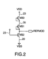
- Fig. 2 is a schematic diagram of a reference voltage circuit useful to the output buffer of Fig. 1.
- Fig. 4 is a waveform diagram showing an output waveform of the output buffer group of Fig. 3 for several different numbers of simultaneously switching outputs.
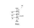
- Fig. 5 is a schematic diagram of an alternate embodiment of an output driver circuit of the output buffer of Fig. 1.
- an output buffer 10.X receives a true and complement logic signal (QX and QBX, respectively) which is buffered to drive an output IOX, suitable for driving a heavily loaded output, and particularly useful as an off-chip pin driver.
- An output enable signal OE provides for a three-state output (a high-impedance state as well as logic "0" and "1").
- a buffer section 25 receives the true logic signal QX and generates an associated signal NPU for driving the gate terminal of the NMOS pull-up transistor of the output driver section 29, which is transistor M19.
- the signal NPU is inverted to form a signal PPU for driving the gate terminal of a PMOS pull-up transistor M20 of the output driver section 29.
- buffer section 25 drives the signal NPU to VSS potential (conveyed on terminal 20) to turn off transistor M19 rather than allowing the signal NPU to follow the true logic signal QX.
- Transistors Ml and M5 are used to limit the current drawn from the VDD power supply during an output transition.
- a reference voltage REFMOD is coupled to the gate terminals of transistors M1 and M5. which are biased by reference voltage REFMOD to operate substantially as constant current sources. Consequently. intermediate node 12 and intermediate node PUCOM function as controlled-conductance "pseudo-VDD" nodes to the remainder of buffer section 25.
- the buffer section 25 would provide the same logic function at node NPU as described above. but without the current limiting afforded by the reference voltage REFMOD.
- the voltage level of REFMOD is preferably designed to compensate for changes in the level of the VDD power supply in order to provide for a constant current level through transistors M1 and M5.
- the level of REFMOD adjusts to a higher voltage to maintain a current constant through transistors Ml and M5. This tends to stabilize the rate at which node NPU is driven high, which otherwise would increase with an increase in the VDD power supply level.
- the voltage level of REFMOD may also be designed to overcompensate for changes in the level of the VDD power supply.
- the level of REFMOD adjusts to lower the current through transistors M1 and M5. This reduces the transient current of the output buffer 10.X by decreasing the output conductance (output pull-up strength) of the M8/M10 inverter. This decreases the rate at which node NPU is driven high, which otherwise would increase with an increase in the VDD power supply level.
- the level of REFMOD adjusts to increase the current through transistors M1 and M5. This increases the pull-up strength of the M8/M10 inverter, and consequently increases the speed of the output buffer 10.X by increasing the rate at which node NPU is driven high, which otherwise would decrease as a result of a decrease in the VDD power supply level.
- transistors M14 and M16 form an inverter which generates (when enabled by the output enable signal OE) a signal on node 18 which is opposite in polarity to the complement logic signal QBX.
- transistor M18 When the output enable signal OE is low (and hence the buffer section 27 is disabled) transistor M18 is turned off to eliminate current flow through the M14/M16 inverter, and transistor M15 is turned on to drive the level of node 18 high.
- the inverter formed by transistors M13 and M17 responds to such a high level on node 18 by driving the PD signal low, thus turning off transistor M21 of output driver 29.
- Fig. 2 is a schematic diagram of a circuit embodiment for generating the reference voltage REFMOD.
- P-channel transistors M30 and M31 and N-channel transistor M32 are series-connected between the VDD power supply conveyed on terminal 23 and the VSS power supply conveyed on terminal 20.
- the gate and drain terminals of transistor M30 are connected together at node 35, and the gate and drain terminals of transistor M31 are connected together at the output node REFMOD. Both transistors M30 and M31 are thus connected in a "diode" configuration.
- Transistor M32 is preferably a narrow, long NMOS transistor which establishes a small bias current therethrough because its gate terminal is biased at VDD potential.
- Output buffer 10.1 receives a true and complement logic signal (Q1 and QB1. respectively) and generates a corresponding output IO1 when enabled by output enable signal OE, and which output buffer 10.1 provides for a high impedance state on output IO1 when disabled by output enable signal OE.
- Output buffers 10.2, 10.3,... 10.8 receive respective logic signals Q2/QB2, Q3/QB3, ... Q8/QB8, and generate respective outputs IO2, IO3, ... IO8.
- the current through transistor M5 is limited, however, by the biasing of reference voltage REFMOD coupled to the gate terminal thereof, as was discussed above.
- the source, gate and drain terminals of the transistor M5 within each of the eight output buffers are each connected to the VDD power supply, the reference voltage REFMOD, and the PUCOM node, respectively.
- the respective transistors M5 from each of the eight output buffers are essentially tied together in parallel by the interconnection of the PUCOM node, and afford a much higher current flow when connected together (in fact, eight times the current for this example) than for a single transistor M5. This increased current affords an increased output pull-up strength for the M8/M 10 inverter.
- the combined current through the eight transistors M5 (the transistor M5 within each of the eight output buffers 10.1, 10.2, ... 10.8) now must be used to drive two NPU signals high (one NPU signal within each of the two high-going output buffers), and so the effective increase in current reduces to four times the value through a single transistor M5. Consequently, the rise time of the two high-going NPU signals is less than the single output transition case above, and which results in a slower rise time for the output IOX.
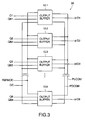
- Fig. 4 is a waveform plot showing the rise time of the output IOX for various numbers of simultaneously switching outputs.
- waveform 41 corresponds to an output IOX when only one output is switching.
- waveform 44 which exhibits a slower rise time than waveform 41, corresponds to each of four simultaneously switching outputs IOX.
- waveform 48 which exhibits an even slower rise time than waveform 44, corresponds to each of eight simultaneously switching outputs IOX.
- the rise time of the output IOX increases as fewer outputs simultaneously switch (when sharing the intermediate nodes between buffers).
- waveform 51 corresponds to an output IOX when only one output is switching, in an output buffer block which does not share node PUCOM between each of the output buffers within the block.
- Waveform 54 represents the rise time when four outputs IOX are switching, again assuming PUCOM is not shared. No speed improvement is achieved, as each output buffer independently determines the delay and rise time of its various signals.
- a similar analysis may be applied to the intermediate node PDCOM which is interconnected (and thus shared) between each of the eight output buffers and which modulates the rise time of the signal PD coupled to the gate of the N-channel pull-down transistor M21. Consequently, the fall time of output IOX of output buffer 10.X is also modulated to take advantage of additional speed as fewer and fewer outputs simultaneously switch.
- Fig. 5 is a schematic diagram of output driver 29a, which is an additional embodiment useful with the output buffer circuit as otherwise indicated in Fig. 1.
- the output buffer output IOX is driven high through two series-connected transistors M20a and M19a.
- Transistor M20a is a PMOS transistor gated by the PPU signal and coupling the I/O power supply voltage VDDIO conveyed on terminal 33 to an intermediate node 60. Separate power supply terminals are used to convey the VDDIO and VSSIO power supply levels to the output driver transistors to help isolate transient noise arising from switching large currents within the output driver, especially transistors M19a and M21a.
- Transistor M19a is a depletion-mode NMOS transistor gated by the NPU signal and which couples the intermediate node 60 to the output IOX.
- enhancement-mode NMOS transistor M21 is gated by the PD signal and couples the output IOX to the l/O power supply voltage VSSIO conveyed on terminal 30.
- a transistor may be conceptualized as having a control terminal which controls the flow of current between a first current handling terminal and a second current handling terminal. An appropriate condition on the control terminal causes a current to flow from/to the first current handling terminal and to/from the second current handling terminal.
- the first current handling terminal may be deemed the collector, the control terminal deemed the base, and the second current handling terminal deemed the emitter.
- a sufficient base current into the base causes a collector-to-emitter current to flow.
- the first current handling terminal may be deemed the emitter, the control terminal deemed the base, and the second current handling terminal deemed the collector.
- a sufficient base current exiting the base causes an emitter-to-collector current to flow.
- An MOS transistor may likewise be conceptualized as having a control terminal which controls the flow of current between a first current handling terminal and a second current handling terminal.
- MOS transistors are frequently discussed as having a drain, a gate, and a source, in most such devices the drain is interchangeable with the source. This is because the layout and semiconductor processing of the transistor is symmetrical (which is typically not the case for bipolar transistors).
- the current handling terminal normally residing at the higher voltage is customarily called the drain.
- the current handling terminal normally residing at the lower voltage is customarily called the source.
- a sufficient voltage on the gate causes a current to therefore flow from the drain to the source.
- a logic gate other than an inverter may be used to generate the signal NPU within buffer section 25.
- the signal conveyed on node 14 may be generated by a variety of embodiments, so long as it follows an input signal when enabled (or gated) and assumes an inactive state when disabled.
- both the intermediate nodes PUCOM and PDCOM may be both interconnected and shared between multiple output buffers. By so doing, the increase in performance, when fewer output buffers are simultaneously switching, is even greater.
Landscapes
- Physics & Mathematics (AREA)
- Engineering & Computer Science (AREA)
- Computer Hardware Design (AREA)
- Computing Systems (AREA)
- General Engineering & Computer Science (AREA)
- Mathematical Physics (AREA)
- Logic Circuits (AREA)
Claims (17)
- Circuit intégré à plusieurs sorties, chaque sortie possédant un tampon de sortie associé (10) comprenant un premier circuit logique (25) et un premier circuit de commande (M19, M20), le premier circuit de commande (M19, M20) répondant à un premier signal de contrôle de commande (NPU) généré par le circuit logique (25) au niveau de l'une de ses sorties pour porter une tension de sortie de tampon à une première tension d'alimentation lorsque le premier signal de contrôle de commande passe à un état actif, la sortie du premier circuit logique (25) incluant un premier noeud intermédiaire formé entre un premier circuit à courant asservi (M5) et une première porte logique (M8, M10), le premier noeud intermédiaire de chaque tampon de sortie (10) étant interconnecté avec des noeuds correspondants dans les premiers circuits logiques respectifs des autres tampons de sortie (10) de telle sorte que la conductance de sortie contrôlée du premier circuit logique (25) et la vitesse de transition résultante de la tension de sortie de tampon lorsqu'elle est portée à la première tension d'alimentation augmente avec un nombre décroissant de sorties commutant simultanément.
- Circuit selon la revendication 1, dans lequel chaque tampon de sortie (10) comprend, de plus : un second circuit logique (27) et un second circuit de commande (M21, M20), le second circuit de commande répondant à un second signal de contrôle de commande (PD) généré par le second circuit logique (27) à l'une de ses sorties pour porter la tension de sortie de tampon à une seconde tension d'alimentation lorsque le second signal de contrôle de commande (PD) passe à un état actif, la sortie du second circuit logique (27) comprenant un second noeud intermédiaire formé entre un second circuit de courant asservi (M11) et une seconde porte logique (M13, M17), le second noeud intermédiaire de chaque tampon de sortie (10) étant interconnecté avec des seconds noeuds correspondants dans les seconds circuits logiques respectifs des autres tampons de sortie (10) de telle sorte que la conductance de sortie contrôlée du second circuit logique (27) et la vitesse de transition résultante de la tension de sortie de tampon lorsqu'elle est portée à la seconde tension d'alimentation augmente avec un nombre décroissant de sorties commutant simultanément.
- Circuit selon la revendication 1 dans lequel la première porte logique (M8, M10) comprend un premier inverseur comportant une borne d'entrée pour recevoir un premier signal de commande de sortie, et une borne de sortie pour y acheminer le premier signal de contrôle de commande ; et dans lequel le premier circuit à courant asservi (M5) est couplé entre le premier inverseur et une borne d'alimentation électrique.
- Circuit selon la revendication 2 dans lequel la seconde porte logique (M13, M17) comprend
un second inverseur comportant une borne d'entrée pour recevoir un second signal de commande de sortie, et une borne de sortie pour y acheminer le second signal de contrôle de commande ; et dans lequel le second circuit à courant asservi (M11) est couplé entre le second inverseur et une borne d'alimentation électrique. - Circuit selon la revendication 3 dans lequel le premier circuit à courant asservi comprend:une borne de tension de référence pour recevoir une tension de référence ;un premier transistor PMOS (M5), le transistor présentant une tension de seuil de canal P, une borne drain/source connectée au premier noeud intermédiaire, une borne de grille connectée à la borne de tension de référence, et une borne source/drain connectée à la première tension d'alimentation ; etdans lequel la tension de référence reçue sur la borne de référence se trouve à une tension approximativement égale à la première tension d'alimentation diminuée d'une valeur reliée à la tension de seuil de canal P.
- Circuit selon la revendication 4 dans lequel le second circuit à courant asservi comprend :
un second transistor PMOS (M11), le transistor présentant une tension de seuil de canal P, une borne drain/source connectée au second noeud intermédiaire, une borne de grille connectée à la borne de tension de référence, et une borne de source/drain connectée à la première tension d'alimentation. - Circuit selon la revendication 1, dans lequel le premier circuit de commande comprend un transistor NMOS (M19, M19a) et un transistor PMOS (M20, M20a) combinés en parallèle ou en série.
- Circuit selon la revendication 1 comprenant, de plus :et dans lequel chaque tampon de sortie (10) comprend:une première borne d'alimentation pour recevoir la première tension d'alimentation ;une seconde borne d'alimentation pour recevoir une seconde tension d'alimentation ;une borne de tension de référence pour recevoir une tension de référence ;une borne de sortie de tension pour y acheminer la tension de sortie de tampon ;un premier transistor MOS (M19, M21) comportant une borne drain/source connectée à la première borne d'alimentation électrique , une borne de grille , et une borne source/drain connectée à la borne de sortie de tampon ;un second transistor MOS (M8, M13) comportant une borne drain/source connectée à la borne de grille du premier transistor MOS, une borne de grille connectée à un premier signal de commande, et une borne source/drain connectée à un premier noeud intermédiaire;un troisième transistor MOS (M5, M11) comportant une borne drain/source connectée au premier noeud intermédiaire, une borne de grille connectée à la borne de tension de référence, et une borne source/drain connectée à la seconde borne d'alimentation électrique.
- Circuit selon la revendication 8 dans lequel les second et troisième transistors MOS comprennent, chacun, un transistor PMOS ou un transistor NMOS, respectivement.
- Circuit selon la revendication 9 dans lequel la première tension d'alimentation transmise sur la première borne d'alimentation est nominalement égale à la seconde tension d'alimentation transmise sur la seconde borne d'alimentation.
- Circuit selon la revendication 9 dans lequel la première tension d'alimentation transmise sur la première borne d'alimentation n'est pas égale à la seconde tension d'alimentation transmise sur la seconde borne d'alimentation.
- Circuit selon la revendication 8, comprenant, de plus :dans lequel chaque tampon de sortie comprend, de plus :une troisième borne d'alimentation pour recevoir une troisième tension d'alimentation ;une quatrième borne d'alimentation pour recevoir une quatrième tension d'alimentation ;un quatrième transistor MOS (M19, M21) comportant une borne drain/source connectée à la borne de sortie de tampon, une borne de grille, et une borne source/drain connectée à la troisième borne d'alimentation ;un cinquième transistor MOS (M8, M13) comportant une borne drain/source connectée à la borne de grille du quatrième transistor MOS ; une borne de grille connectée à un second signal de commande et une borne source/drain connectée à un second noeud intermédiaire ;un sixième transistor MOS (M5, M11) comportant une borne drain/source connectée au second noeud intermédiaire, une borne de grille connectée à la borne de tension de référence, et une borne source/drain connectée à la quatrième borne d'alimentation ; etdans lequel les seconds noeuds intermédiaires respectifs à l'intérieur de chacun des tampons de sortie respectifs sont interconnectés.
- Circuit selon la revendication 12 dans lequel les premiers noeuds respectifs intermédiaires et les seconds noeuds respectifs intermédiaires à l'intérieur de chacun des tampons de sortie respectifs sont tous interconnectés.
- Circuit selon la revendication 1, comprenant, de plus :une premièreborne d'alimentation pour recevoir la première tension d'alimentation ;une seconde borne d'alimentation pour recevoir une seconde tension d'alimentation ;une troisième borne d'alimentation pour recevoir la première tension d'alimentation ;une quatrième borne d'alimentation pour recevoir la seconde tension d'alimentation ;une borne de référence pour recevoir une tension de référence ;et dans lequel chaque tampon de sortie comprend ;une borne de sortie de tampon pour y acheminer la tension de sortie de tampon ;une seconde porte logique (M3, M4, M6, M9) comportant des première et seconde entrées et comportant une sortie, ladite première entrée répondant à un signal de commande de polarité de sortie vrai , ladite seconde entrée répondant à un signal de commande de validation de sortie de tampon, ladite seconde porte logique étant couplée à la première borne d'alimentation par l'intermédiaire d'un second circuit à courant asservi (M1) et couplée à la seconde borne d'alimentation, ladite seconde porte logique et ledit second circuit à courant asservi définissant entre eux un second noeud intermédiaire (12) ;la première porte logique (M8, M10) ayant une entrée couplée à la seconde sortie de porte logique et ayant une sortie, ladite première porte logique étant couplée à la première borne d'alimentation à travers le premier circuit de courant asservi (M5) ;le premier circuit de commande (M19, M20) comportant une entrée répondant à la première sortie de porte logique et une sortie couplée à la borne de sortie de tampon, ledit premier cicuit de commande étant couplé à la troisième borne d'alimentation ;une troisième porte logique (M14, M15, M16, M18) comportant des première et seconde entrées et comportant une sortie, ladite première entrée répondant à un signal de commande de polarité de sortie complémentaire, ladite seconde entrée répondant au signal de commande de validation de sortie de tampon, ladite troisième porte logique étant couplée à la première borne d'alimentation par un troisième circuit de courant asservi (M12), et étant couplée à la seconde borne d'alimentation, ladite troisième porte logique et ledit troisième circuit à courant asservi définissant entre eux un troisième noeud intermédiaire (16) ;une quatrième porte logique (M13, M17) comportant une entrée couplée à la troisième sortie de porte logique et comportant une sortie, ladite quatrième porte logique étant couplée à la première borne d'alimentation à travers un quatrième circuit à courant asservi (M11), et étant couplée à la seconde borne d'alimentation, ladite quatrième porte logique et ledit quatrième circuit à courant asservi définissant entre eux un quatrième noeud intermédiaire ;un second circuit de commande (M21, M20) comportant une entrée répondant à la quatrième sortie de porte logique, présentant une sortie couplée à la borne de sortie de tampon, ledit circuit de commande étant couplé à la quatrième borne d'alimentation ;dans lequel les troisièmes noeuds respectifs intermédiaires à l'intérieur de chaque tampon de la pluralité de tampons de sortie sont interconnectés ; etdans lequel les quatrièmes noeuds respectifs intermédiaires à l'intérieur de chaque tampon de la pluralité de tampons de sortie sont interconnectés.
- Circuit selon la revendication 14 dans lequel le premier circuit de commande à l'intérieur de chaque tampon de sortie comprend :un transistor NMOS (M19) présentant une borne drain/source couplée à la troisième borne d'alimentation, une borne de grille couplée à la première entrée de circuit de commande, et une borne source/drain couplée à la première sortie de circuit de commande ;un inverseur (M2, M7) présentant une entrée couplée à la première entrée de circuit de commande, et comportant une sortie ;un transistor PMOS (M2) présentant une borne de drain couplée à la première sortie de circuit de commande, une borne de grille couplée à la sortie d'inverseur, et une borne source/drain couplée à la troisième borne d'alimentation électrique.
- Circuit selon la revendication 14 dans lequel le premier circuit de commande à l'intérieur de chaque tampon de sortie comprend :un transistor NMOS (M19) comportant une borne drain/source , une borne de grille couplée à la première entrée de circuit de commande, et une borne source/drain couplée à la première sortie de circuit de commande ;un inverseur (M2,M7) présentant une entrée couplée à la première entrée de circuit de commande, et comportant une sortie ;un transistor PMOS (M20) présentant une borne de drain couplée à la borne drain/source du transistor NMOS, une borne de grille couplée à la sortie de l'inverseur, et une borne source/drain couplée à la troisième borne d'alimentation.
- Circuit selon la revendication 14 dans lequel au moins l'un des premier, second, troisième et quatrième circuits à courant asservi comprend un transistor PMOS ayant une tension de seuil de canal P, une borne drain/source connectée, respectivement, au premier, second, troisième, et quatrième noeuds intermédiaires respectifs, une borne de grille connectée à la borne de référence, et une borne source/drain connectée à la première borne d'alimentation électrique, et dans lequel la tension de référence transmise sur la borne de référence se trouve à une tension approximativement égale à la première tension d'alimentation reçue sur la première borne d'alimentation diminuée d'une valeur reliée à la tension de seuil de canal P.
Applications Claiming Priority (3)
| Application Number | Priority Date | Filing Date | Title |
|---|---|---|---|
| US52306895A | 1995-09-01 | 1995-09-01 | |
| US523068 | 1995-09-01 | ||
| PCT/US1996/011554 WO1997009784A1 (fr) | 1995-09-01 | 1996-07-11 | Tampon de sortie a noeuds intermediaires partages |
Publications (2)
| Publication Number | Publication Date |
|---|---|
| EP0847623A1 EP0847623A1 (fr) | 1998-06-17 |
| EP0847623B1 true EP0847623B1 (fr) | 2001-03-07 |
Family
ID=24083531
Family Applications (1)
| Application Number | Title | Priority Date | Filing Date |
|---|---|---|---|
| EP96923751A Expired - Lifetime EP0847623B1 (fr) | 1995-09-01 | 1996-07-11 | Tampon de sortie a noeuds intermediaires partages |
Country Status (6)
| Country | Link |
|---|---|
| US (1) | US5717342A (fr) |
| EP (1) | EP0847623B1 (fr) |
| JP (1) | JPH11512572A (fr) |
| KR (1) | KR19990044240A (fr) |
| DE (1) | DE69612007T2 (fr) |
| WO (1) | WO1997009784A1 (fr) |
Families Citing this family (19)
| Publication number | Priority date | Publication date | Assignee | Title |
|---|---|---|---|---|
| CA2171052C (fr) * | 1995-09-29 | 2001-05-15 | Pmc-Sierra Ltd. | Pilote de sortie a trois etats pour logique cmos fonctionnant sous 3,3 ou 5 volts |
| US5917358A (en) * | 1997-12-09 | 1999-06-29 | Motorola, Inc. | Method and output buffer with programmable bias to accommodate multiple supply voltages |
| US6236237B1 (en) * | 1998-02-27 | 2001-05-22 | Altera Corporation | Output buffer predriver with edge compensation |
| US6181166B1 (en) * | 1998-06-19 | 2001-01-30 | Intel Corporation | Tristate driver for integrated circuit interconnects |
| DE10136320B4 (de) * | 2001-07-26 | 2008-05-15 | Infineon Technologies Ag | Anordnung und Verfahren zum Umschalten von Transistoren |
| US6996640B1 (en) | 2001-08-07 | 2006-02-07 | Adaptec, Inc. | Method and system for asynchronously transferring data |
| US6664805B2 (en) | 2002-01-30 | 2003-12-16 | Agilent Technologies, Inc. | Switched capacitor piecewise linear slew rate control methods for output devices |
| KR100498453B1 (ko) * | 2002-11-04 | 2005-07-01 | 삼성전자주식회사 | 출력 데이터의 스큐를 감소시킬 수 있는 출력버퍼 회로 |
| KR100928750B1 (ko) | 2003-08-07 | 2009-11-25 | 매그나칩 반도체 유한회사 | 버퍼 장치 및 그의 구동 방법 |
| US7005886B2 (en) * | 2004-04-30 | 2006-02-28 | Agilent Technologies, Inc. | Tristateable CMOS driver with controlled slew rate for integrated circuit I/O pads |
| US7088129B2 (en) * | 2004-04-30 | 2006-08-08 | Avago Technologies General Ip (Singapore) Pte. Ltd. | Hybrid binary/thermometer code for controlled-voltage integrated circuit output drivers |
| DE102004049194B3 (de) | 2004-10-08 | 2006-02-02 | Infineon Technologies Ag | Vorstufe für einen externen Treiber (OCD) |
| US20070024317A1 (en) * | 2005-07-29 | 2007-02-01 | Hansen James E | Apparatus for obtaining precision integrated resistors |
| JP2007188395A (ja) * | 2006-01-16 | 2007-07-26 | Elpida Memory Inc | クロック信号発生回路 |
| US7471121B2 (en) * | 2006-12-21 | 2008-12-30 | System General Corp. | Transistor drive circuit of power converter operating in a wide voltage range |
| JP2011018438A (ja) * | 2010-09-13 | 2011-01-27 | Renesas Electronics Corp | 半導体装置 |
| CN102684458A (zh) * | 2012-05-09 | 2012-09-19 | 矽力杰半导体技术(杭州)有限公司 | 一种功率开关管的驱动电路以及应用其的开关电源电路 |
| KR102555212B1 (ko) | 2017-12-29 | 2023-07-12 | 엘지디스플레이 주식회사 | 발광 표시 장치 |
| CN119440927B (zh) * | 2024-11-04 | 2025-09-26 | 宝德计算机系统股份有限公司 | 一种自动验证npu驱动稳定性以及性能的方法及装置 |
Family Cites Families (14)
| Publication number | Priority date | Publication date | Assignee | Title |
|---|---|---|---|---|
| JPS59133624A (ja) * | 1983-01-20 | 1984-08-01 | Sharp Corp | インタ−フエイス方式 |
| US4743781A (en) * | 1986-07-03 | 1988-05-10 | International Business Machines Corporation | Dotting circuit with inhibit function |
| US5066873A (en) * | 1989-12-04 | 1991-11-19 | Altera Corporation | Integrated circuits with reduced switching noise |
| US5111074A (en) * | 1990-07-26 | 1992-05-05 | Regents Of The University Of Minnesota | Multi-input compound function complementary noise-immune logic |
| US5111064A (en) * | 1990-09-05 | 1992-05-05 | Vlsi Technology, Inc. | Slow ramp high drive output pad |
| JPH04146650A (ja) * | 1990-10-08 | 1992-05-20 | Mitsubishi Electric Corp | 半導体集積回路装置 |
| US5221865A (en) * | 1991-06-21 | 1993-06-22 | Crosspoint Solutions, Inc. | Programmable input/output buffer circuit with test capability |
| US5583457A (en) * | 1992-04-14 | 1996-12-10 | Hitachi, Ltd. | Semiconductor integrated circuit device having power reduction mechanism |
| JPH05335927A (ja) * | 1992-06-02 | 1993-12-17 | Toshiba Corp | 半導体装置 |
| US5319252A (en) * | 1992-11-05 | 1994-06-07 | Xilinx, Inc. | Load programmable output buffer |
| US5479123A (en) * | 1993-06-18 | 1995-12-26 | Digital Equipment Corporation | Externally programmable integrated bus terminator for optimizing system bus performance |
| JP3507534B2 (ja) * | 1993-10-20 | 2004-03-15 | 株式会社東芝 | 半導体装置 |
| EP0690510B1 (fr) * | 1994-06-28 | 1998-05-06 | Nippon Telegraph And Telephone Corporation | Circuit logique SOI (silicium sur isolant) à basse tension |
| US5604454A (en) * | 1995-09-29 | 1997-02-18 | Motorola Inc. | Integrated circuit with low output buffer energy consumption and related method |
-
1996
- 1996-07-11 KR KR1019980701476A patent/KR19990044240A/ko not_active Withdrawn
- 1996-07-11 DE DE69612007T patent/DE69612007T2/de not_active Expired - Fee Related
- 1996-07-11 JP JP9511179A patent/JPH11512572A/ja active Pending
- 1996-07-11 WO PCT/US1996/011554 patent/WO1997009784A1/fr not_active Ceased
- 1996-07-11 EP EP96923751A patent/EP0847623B1/fr not_active Expired - Lifetime
- 1996-11-22 US US08/745,410 patent/US5717342A/en not_active Expired - Lifetime
Also Published As
| Publication number | Publication date |
|---|---|
| WO1997009784A1 (fr) | 1997-03-13 |
| KR19990044240A (ko) | 1999-06-25 |
| US5717342A (en) | 1998-02-10 |
| EP0847623A1 (fr) | 1998-06-17 |
| DE69612007D1 (de) | 2001-04-12 |
| DE69612007T2 (de) | 2001-10-25 |
| JPH11512572A (ja) | 1999-10-26 |
Similar Documents
| Publication | Publication Date | Title |
|---|---|---|
| EP0847623B1 (fr) | Tampon de sortie a noeuds intermediaires partages | |
| US5206544A (en) | CMOS off-chip driver with reduced signal swing and reduced power supply disturbance | |
| US6825692B1 (en) | Input buffer for multiple differential I/O standards | |
| US7196547B2 (en) | Level shifter and buffer circuit | |
| JP3093380B2 (ja) | 半導体集積回路における信号出力回路 | |
| US6593795B2 (en) | Level adjustment circuit and data output circuit thereof | |
| US6759876B2 (en) | Semiconductor integrated circuit | |
| US5598107A (en) | Current switching circuit having reduced current noise operation | |
| EP0225249B1 (fr) | Circuit de commutation de courant CMOS | |
| US5239211A (en) | Output buffer circuit | |
| US5929679A (en) | Voltage monitoring circuit capable of reducing power dissipation | |
| EP0346898B1 (fr) | Circuit de commutation d'alimentation | |
| US4725982A (en) | Tri-state buffer circuit | |
| US4996449A (en) | Output circuit having high speed operation and low power dissipation | |
| US6812743B2 (en) | Input buffer of differential amplification type in semiconductor device | |
| US5317213A (en) | Level converter with delay circuitry used to increase switching speed | |
| US6621329B2 (en) | Semiconductor device | |
| US6351175B1 (en) | Mode select circuit | |
| US5059822A (en) | Method and apparatus for controlling noise on power supply buses | |
| EP1717955A1 (fr) | Circuit tampon | |
| US5280204A (en) | ECI compatible CMOS off-chip driver using feedback to set output levels | |
| JPH04329023A (ja) | 出力バッファ回路 | |
| US5118972A (en) | BiCMOS gate pull-down circuit | |
| KR0153067B1 (ko) | 단일 전원 차동 회로 | |
| US6329842B1 (en) | Output circuit for electronic devices |
Legal Events
| Date | Code | Title | Description |
|---|---|---|---|
| PUAI | Public reference made under article 153(3) epc to a published international application that has entered the european phase |
Free format text: ORIGINAL CODE: 0009012 |
|
| 17P | Request for examination filed |
Effective date: 19980211 |
|
| AK | Designated contracting states |
Kind code of ref document: A1 Designated state(s): DE FR GB |
|
| GRAG | Despatch of communication of intention to grant |
Free format text: ORIGINAL CODE: EPIDOS AGRA |
|
| 17Q | First examination report despatched |
Effective date: 20000629 |
|
| GRAG | Despatch of communication of intention to grant |
Free format text: ORIGINAL CODE: EPIDOS AGRA |
|
| GRAH | Despatch of communication of intention to grant a patent |
Free format text: ORIGINAL CODE: EPIDOS IGRA |
|
| GRAH | Despatch of communication of intention to grant a patent |
Free format text: ORIGINAL CODE: EPIDOS IGRA |
|
| GRAA | (expected) grant |
Free format text: ORIGINAL CODE: 0009210 |
|
| AK | Designated contracting states |
Kind code of ref document: B1 Designated state(s): DE FR GB |
|
| PG25 | Lapsed in a contracting state [announced via postgrant information from national office to epo] |
Ref country code: FR Free format text: LAPSE BECAUSE OF FAILURE TO SUBMIT A TRANSLATION OF THE DESCRIPTION OR TO PAY THE FEE WITHIN THE PRESCRIBED TIME-LIMIT Effective date: 20010307 |
|
| REF | Corresponds to: |
Ref document number: 69612007 Country of ref document: DE Date of ref document: 20010412 |
|
| RAP2 | Party data changed (patent owner data changed or rights of a patent transferred) |
Owner name: VANTIS CORPORATION |
|
| PGFP | Annual fee paid to national office [announced via postgrant information from national office to epo] |
Ref country code: DE Payment date: 20010702 Year of fee payment: 6 |
|
| PGFP | Annual fee paid to national office [announced via postgrant information from national office to epo] |
Ref country code: GB Payment date: 20010711 Year of fee payment: 6 |
|
| EN | Fr: translation not filed | ||
| REG | Reference to a national code |
Ref country code: GB Ref legal event code: IF02 |
|
| PLBE | No opposition filed within time limit |
Free format text: ORIGINAL CODE: 0009261 |
|
| STAA | Information on the status of an ep patent application or granted ep patent |
Free format text: STATUS: NO OPPOSITION FILED WITHIN TIME LIMIT |
|
| 26N | No opposition filed | ||
| PG25 | Lapsed in a contracting state [announced via postgrant information from national office to epo] |
Ref country code: GB Free format text: LAPSE BECAUSE OF NON-PAYMENT OF DUE FEES Effective date: 20020711 |
|
| REG | Reference to a national code |
Ref country code: GB Ref legal event code: 732E |
|
| PG25 | Lapsed in a contracting state [announced via postgrant information from national office to epo] |
Ref country code: DE Free format text: LAPSE BECAUSE OF NON-PAYMENT OF DUE FEES Effective date: 20030201 |
|
| GBPC | Gb: european patent ceased through non-payment of renewal fee |
Effective date: 20020711 |