EP0848299A2 - Dispositif porte-objet et appareil de projection optique - Google Patents
Dispositif porte-objet et appareil de projection optique Download PDFInfo
- Publication number
- EP0848299A2 EP0848299A2 EP97310110A EP97310110A EP0848299A2 EP 0848299 A2 EP0848299 A2 EP 0848299A2 EP 97310110 A EP97310110 A EP 97310110A EP 97310110 A EP97310110 A EP 97310110A EP 0848299 A2 EP0848299 A2 EP 0848299A2
- Authority
- EP
- European Patent Office
- Prior art keywords
- stage
- displacement
- material support
- predetermined plane
- storage
- Prior art date
- Legal status (The legal status is an assumption and is not a legal conclusion. Google has not performed a legal analysis and makes no representation as to the accuracy of the status listed.)
- Withdrawn
Links
Images


Classifications
-
- G—PHYSICS
- G03—PHOTOGRAPHY; CINEMATOGRAPHY; ANALOGOUS TECHNIQUES USING WAVES OTHER THAN OPTICAL WAVES; ELECTROGRAPHY; HOLOGRAPHY
- G03F—PHOTOMECHANICAL PRODUCTION OF TEXTURED OR PATTERNED SURFACES, e.g. FOR PRINTING, FOR PROCESSING OF SEMICONDUCTOR DEVICES; MATERIALS THEREFOR; ORIGINALS THEREFOR; APPARATUS SPECIALLY ADAPTED THEREFOR
- G03F9/00—Registration or positioning of originals, masks, frames, photographic sheets or textured or patterned surfaces, e.g. automatically
- G03F9/70—Registration or positioning of originals, masks, frames, photographic sheets or textured or patterned surfaces, e.g. automatically for microlithography
- G03F9/7003—Alignment type or strategy, e.g. leveling, global alignment
- G03F9/7023—Aligning or positioning in direction perpendicular to substrate surface
- G03F9/7026—Focusing
-
- G—PHYSICS
- G03—PHOTOGRAPHY; CINEMATOGRAPHY; ANALOGOUS TECHNIQUES USING WAVES OTHER THAN OPTICAL WAVES; ELECTROGRAPHY; HOLOGRAPHY
- G03F—PHOTOMECHANICAL PRODUCTION OF TEXTURED OR PATTERNED SURFACES, e.g. FOR PRINTING, FOR PROCESSING OF SEMICONDUCTOR DEVICES; MATERIALS THEREFOR; ORIGINALS THEREFOR; APPARATUS SPECIALLY ADAPTED THEREFOR
- G03F7/00—Photomechanical, e.g. photolithographic, production of textured or patterned surfaces, e.g. printing surfaces; Materials therefor, e.g. comprising photoresists; Apparatus specially adapted therefor
- G03F7/70—Microphotolithographic exposure; Apparatus therefor
- G03F7/70216—Mask projection systems
- G03F7/70358—Scanning exposure, i.e. relative movement of patterned beam and workpiece during imaging
-
- G—PHYSICS
- G03—PHOTOGRAPHY; CINEMATOGRAPHY; ANALOGOUS TECHNIQUES USING WAVES OTHER THAN OPTICAL WAVES; ELECTROGRAPHY; HOLOGRAPHY
- G03F—PHOTOMECHANICAL PRODUCTION OF TEXTURED OR PATTERNED SURFACES, e.g. FOR PRINTING, FOR PROCESSING OF SEMICONDUCTOR DEVICES; MATERIALS THEREFOR; ORIGINALS THEREFOR; APPARATUS SPECIALLY ADAPTED THEREFOR
- G03F7/00—Photomechanical, e.g. photolithographic, production of textured or patterned surfaces, e.g. printing surfaces; Materials therefor, e.g. comprising photoresists; Apparatus specially adapted therefor
- G03F7/70—Microphotolithographic exposure; Apparatus therefor
- G03F7/70425—Imaging strategies, e.g. for increasing throughput or resolution, printing product fields larger than the image field or compensating lithography- or non-lithography errors, e.g. proximity correction, mix-and-match, stitching or double patterning
-
- G—PHYSICS
- G03—PHOTOGRAPHY; CINEMATOGRAPHY; ANALOGOUS TECHNIQUES USING WAVES OTHER THAN OPTICAL WAVES; ELECTROGRAPHY; HOLOGRAPHY
- G03F—PHOTOMECHANICAL PRODUCTION OF TEXTURED OR PATTERNED SURFACES, e.g. FOR PRINTING, FOR PROCESSING OF SEMICONDUCTOR DEVICES; MATERIALS THEREFOR; ORIGINALS THEREFOR; APPARATUS SPECIALLY ADAPTED THEREFOR
- G03F7/00—Photomechanical, e.g. photolithographic, production of textured or patterned surfaces, e.g. printing surfaces; Materials therefor, e.g. comprising photoresists; Apparatus specially adapted therefor
- G03F7/70—Microphotolithographic exposure; Apparatus therefor
- G03F7/70691—Handling of masks or workpieces
- G03F7/707—Chucks, e.g. chucking or un-chucking operations or structural details
-
- G—PHYSICS
- G03—PHOTOGRAPHY; CINEMATOGRAPHY; ANALOGOUS TECHNIQUES USING WAVES OTHER THAN OPTICAL WAVES; ELECTROGRAPHY; HOLOGRAPHY
- G03F—PHOTOMECHANICAL PRODUCTION OF TEXTURED OR PATTERNED SURFACES, e.g. FOR PRINTING, FOR PROCESSING OF SEMICONDUCTOR DEVICES; MATERIALS THEREFOR; ORIGINALS THEREFOR; APPARATUS SPECIALLY ADAPTED THEREFOR
- G03F7/00—Photomechanical, e.g. photolithographic, production of textured or patterned surfaces, e.g. printing surfaces; Materials therefor, e.g. comprising photoresists; Apparatus specially adapted therefor
- G03F7/70—Microphotolithographic exposure; Apparatus therefor
- G03F7/70691—Handling of masks or workpieces
- G03F7/70716—Stages
Definitions
- the present invention relates to a stage apparatus and a projection optical apparatus. More particularly, the present invention relates to a stage apparatus including a material support capable of positioning a material piece carried thereon with at least three degrees of freedom, and to a projection optical apparatus including such a stage apparatus used as a positioning stage for a material piece.
- a projection optical apparatus is a projection exposure apparatus, such as a stepper, for use in a photolithographic process forming a part of the fabrication process of semiconductor devices, liquid crystal displays or other products.
- lens inspection equipment for measuring various aberrations associated with a projection optical system (or projection lens) equipped for such a projection exposure apparatus.
- stage apparatus is typically used for positioning a material piece or substrate having a photosensitive layer coated on its surface.
- the substrate may typically comprise a silicon wafer or a glass plate (referred to simply as a "wafer” hereinafter).
- One common stage apparatus comprises an XY-stage capable of two-dimensional movement in a plane (typically, an XY-plane) and a material support (or Z-stage) for supporting a material piece or wafer thereon, the material support being mounted on the XY-stage and capable of displacing in the Z-direction perpendicular to the XY-plane.
- a demagnification projection exposure apparatus of the step-and-repeat type (commonly referred to as a "stepper").
- the wafer is moved or stepped to the next shot-area and the process is repeated until the entire surface of the wafer (or every shot-area on the wafer) has been processed to have reticle patterns transferred onto it.
- the stepping movement of the wafer is produced by the two-dimensional movement or translation of the XY-stage supporting that wafer.
- a typical demagnification exposure apparatus uses a projection lens having a large numerical aperture (NA), its depth of focus is so small that a certain, appropriate mechanism must be provided for bringing with precision the surface of the wafer to a position at which it will be coincident with the image plane of the reticle pattern defined by the projection lens (such a mechanism may be, for example, an auto-focussing mechanism or a levelling mechanism).
- a mechanism may be, for example, an auto-focussing mechanism or a levelling mechanism.
- various aberrations such as, variation in depth of focus, curvature of image plane, tilt of image plane and others
- Wafer-flatness measurement as well as the measurement of aberrations with the projection lens by lens inspection equipment, have been typically performed by using the positions of the moving XY-stage as the reference for the measurement.
- the XY-stage is driven so as to sequentially move the wafer into a number of predetermined measurement points arranged in a rectangular array or matrix, and the height (or the position in the Z-direction) of the surface of the wafer is measured at each measurement point.
- the Z-direction is perpendicular to the plane in which the XY-stage moves and is usually defined as the direction along the optical axis of the projection optical system.
- the surface of the wafer or material piece carried by the XY-stage may rise and sink (or displace in the Z-direction) while the XY-stage is driven (or more exactly an X-stage and/or a Y-stage, together composing the XY-stage, are driven) to move the wafer in the XY-plane.
- the drive mechanism for the stage comprises a feed screw in threading engagement with the stage and an electric motor for rotating the feed screw
- such displacement in the Z-direction may be possibly caused by various factors, including minute irregularities in the nominally flat bearing surface along which the stage is guided, an inevitable play between the feed screw and the stage engaging with each other, some distortion induced in the feed screw, and others.
- the rise/sink of the stage produced when the stage is moved into different positions, or the displacement characteristic of the stage often causes errors in the results of the wafer-flatness measurement and the lens-aberration measurement.
- the yaw of wafers which may be separately measured with ease by a yaw-measuring interferometer, it has been impossible to separately measure the displacement characteristic of the stage (or the rise/sink of the stage), with the result that the wafer-flatness measurement and the lens-aberration measurement have been performed so far, allowing for such errors.
- stage apparatus which may provide an improved measurement accuracy in various measurement processes in which the positions of the moving stage are used as a reference for the measurement.
- a stage apparatus comprising: a first stage movable in two orthogonal directions in a predetermined plane; a material support mounted on the first stage and capable of minute displacement in the direction along a first axis perpendicular to the predetermined plane; a measuring device for measuring coordinates of the position of the material support mounted on the first stage in the two orthogonal directions; and a storage for storing displacement data indicative of displacement of the material support in the direction along the first axis, as caused by movement of the first stage, in association with coordinates of corresponding position of the material support.
- this stage apparatus when the material support is moved along with the first stage, the coordinates of the position of the material support are measured by the measuring device. At the same time, displacement of the material support in the direction along the first axis as caused by the movement of the first stage is stored in the storage in association with coordinates of corresponding position of the material support.
- the displacement data stored in the storage may be any of data indicative of displacements of the material support in the direction along the first axis corresponding to a number of positions of the material support, irrespective of the method of performing the measurement. More particularly, the displacement data stored in the storage may be data as derived by arithmetic operation from a distance data indicative of a distance of a surface of a plane-parallel surface-mirror placed on the material support from a predetermined reference point, as measured in the direction along the first axis at each of measurement points while the first stage is moved with step intervals in the predetermined plane. In this case, it is preferable to measure, in advance, the flatness of the surface of the plane-parallel surface-mirror by an appropriate surface shape measuring device, such as a Fizeau interferometer.
- an appropriate surface shape measuring device such as a Fizeau interferometer.
- correction to the results of the flatness measurement process may be effected after the flatness measurement process itself is completed as with a conventional correction method, by subtracting correction amount (derived from the displacement data stored) at the corresponding position in the predetermined plane, from the measured value at each measurement point.
- correction may be made by correcting the position of the material support in the direction along the first axis through a real-time correction operation using the correction amount just measured, during the flatness measurement process.
- the stage apparatus may further comprise an adjustor for adjusting, while the first stage is moved, the position of the material support in the direction along the first axis, depending on the amount of such displacement of the material support in the direction along the first axis that is indicated by the displacement data and that corresponds to the current position of the material support.
- the position of the material support in the direction along the first axis may be corrected depending on the amount of such displacement of the material support that corresponds to the current position of the material support by means of the adjustor. Therefore, the flatness measurement process and other measurement processes may be performed under an ideal condition effectively with no rise/sink of the first stage, and thus with great precision.
- the stage apparatus may further comprise an arithmetic operation device for performing interpolation on the displacement data in the storage to derive the amount of such displacement of the material support in the direction along the first axis that corresponds to the current position of the material support, when the first stage has been moved to such a position for which the displacement data in the storage contains no indication of displacement.
- a projection optical apparatus comprising: a stage apparatus for supporting a substrate; a mask having a pattern formed thereon; an illumination system for illuminating the mask with an exposure light beam; a projection optical system for projecting the pattern formed on the mask onto the substrate with the exposure light beam; and the stage apparatus having: a first stage movable in two orthogonal directions in a predetermined plane; a material support for supporting a substrate, the material support being mounted on the first stage and capable of minute displacement in the direction along a first axis perpendicular to the predetermined plane; a measuring device for measuring coordinates of the position of the material support mounted on the first stage in the two orthogonal directions; and a storage for storing displacement data indicative of displacement of the material support in the direction along the first axis, as caused by movement of the first stage, in association with coordinates of corresponding position of the material support.
- the stage apparatus for use as a stage for positioning the photosensitized substrate, correction may be effected to the position of the material support and/or the measured values obtained through the flatness measurement process and other measurement processes based on the displacement data stored in the storage and indicative of displacements of the material support in the direction along the first axis at a number of measurement points.
- the measurement accuracy with the flatness measurement process performed on the photosensitized substrate placed on the material support may be improved.
- the measurement of aberrations with a projection lens may be performed with great accuracy as well.
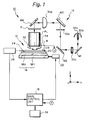
- Fig. 1 is a schematic of a projection exposure apparatus 10 according to an embodiment of the present invention, which is a representative of various projection optical apparatus with which a stage apparatus according to the present invention may be used.
- the projection exposure apparatus 10 includes a wafer stage 12 for carrying thereon a photosensitized substrate or wafer W, a projection optical system PL disposed above the wafer stage 12, a master matrix of a pattern or reticle R held on a reticle holder (not shown) and disposed above the projection optical system PL, an illumination system 14 for illuminating the reticle R with an exposure light beam, and a main control unit 16 for providing general control of the entire projection exposure apparatus 10.
- the wafer stage 12 comprises a first stage or XY-stage 18, which in turn comprises a Y-stage 18Y supported on a base (not shown) and movable in the Y-direction (perpendicular to the drawing sheet surface of Fig. 1) and an X-stage 18X supported on the Y-stage 18Y and movable in the X-direction (left-to-right direction as viewed in Fig. 1) perpendicular to the Y-direction.
- the wafer stage 12 further comprises a material support 20 carried on the X-stage 18X and movable in the Z-direction (perpendicular to the XY-plane) within a predetermined displacement range of, for example, 100 ⁇ m.
- the Y-stage 18Y, the X-stage 18X and the material support 20 are driven by means of a drive unit 22 for their movements in their own moving directions.
- the drive unit 22 includes a pair of drive mechanisms, one for each of the Y-stage 18Y and the X-stage 18X.
- the drive mechanism comprises a combination of a feed screw and an electric motor for rotating the feed screw.
- the drive unit 22 further includes a third drive mechanism (not shown) associated with the material support 20 for driving it to move or displace in the Z-direction.
- the material support 20 and the associated drive mechanism together constitute a Z-stage for driving or displacing the wafer W on the material support 20 in the Z-direction.
- the drive mechanism associated with the material support 20 includes a built-in encoder for measuring the displacement of the material support 20 in the Z-direction, and the drive unit 22 uses the measured values output from the encoder when it drives the material support 20 in the Z-direction.
- a pair of movable mirrors 24 (only one of them is shown in Fig. 1) are fixedly mounted on the material support 20.
- a pair of corresponding position-measuring devices or laser interferometer units 26 (again only one of them is shown in Fig. 1) are disposed each facing the associated one of the movable mirrors 24 for emitting a measuring beam (laser beam) toward the associated movable mirror 24 and using the reflection beam therefrom to measure the position of the material support 20 in the direction along its measuring beam.
- the movable mirrors 24 include an X-direction movable mirror having its mirror surface extending perpendicular to the X-axis and a Y-direction movable mirror having its mirror surface extending perpendicular to the Y-axis.
- the interferometer units 26 include an X-direction laser interferometer unit for measuring the position of the material support 20 in the X-direction and a Y-direction laser interferometer unit for measuring the position of the material support 20 in the Y-direction.
- Fig. 1 only one movable mirror 24 and only one interferometer unit 26 are shown as representatives of the pairs.
- the shown combination of the laser interferometer unit 26 and the movable mirror 24 provides the measurements of the two-dimensional, XY-coordinates of the position of the material support 20 with a high resolution of, for example, 0.01 ⁇ m.
- the measurements from the laser interferometer 26 are supplied to the main control unit 16.
- a wafer holder 28 is mounted on the material support 20.
- the material piece or wafer W is held on the wafer holder 28 by means of vacuum suction, which may be provided, for example, by a vacuum chuck.
- the illumination system 14 comprises a mercury lamp 30a serving as an illumination light source, an ellipsoidal reflector 30b, mirrors M1, M2, M3 and M4, a shutter 30c, a blind 30d, a condensor lens 30e and other elements not shown for simplicity.
- the mercury lamp 30a emits illumination rays, which are collected by the ellipsoidal reflector 30b into the region around the secondary focal point of the ellipsoidal reflector 30b. From the collected rays, only light of a selected wavelength for exposure purpose is passed through a suitable wavelength selector element (not shown) to form an illumination light beam, which then strikes on and is reflected by the mirror M1 into the shutter 30c.
- the wavelength may be selected, for example, to 364 nm where the light of i-line from the mercury lamp output should be used.
- the illumination light beam (which is also an exposure light beam) is allowed to pass through the shutter 30c and reflected by the mirror M2 into an optical integrator (not shown) which may comprise a fly's eye lens.
- the illumination beam then passes through the blind 30d, is reflected by the mirror M3, passes through a relay lens system (not shown) and through the condensor lens 30e, and is again reflected by the mirror M4 to illuminate the reticle R.
- the optical integrator serves to improve uniformness in illuminance over the entire surface of the reticle R.
- the blind 30d is disposed at a position which is conjugate to the position of the pattern bearing surface of the reticle R and has an aperture which defines the outline of the illumination area produced on the surface of the reticle R.
- the reticle R is held on the reticle holder (not shown).
- the position of the reticle R is adjustable within an XY-plane by means of an adjustor mechanism (not shown).
- the reticle R has a circuit pattern (not shown) drawn on the under surface thereof, which extends in a plane which will be substantially, optically conjugate to the plane of the surface of the wafer W.
- the projection optical system PL is mounted on and supported by a body column (not shown) of the projection exposure apparatus 10, with its optical axis extending in the Z-direction.
- the projection optical system PL used in the disclosed embodiment has double-side telecentricity with a selected demagnification ratio ⁇ (which may be selected, for example, to 1/4 or 1/5).
- a focus detection system of the oblique incidence type is disposed by the projection optical system PL and comprises a light-beam-sending unit 32 and a light-beam-receiving unit 34.
- the focus detection system (32, 34) serves to measure the displacement of the surface of the wafer W in the direction along the optical axis of the projection optical system PL (thus, the displacement is the out-of-focus distance.)
- the detection signals output from the focus detection system (32, 34) are supplied to the main control unit 16.
- the main control unit 16 comprises a microcomputer (alternatively, it may comprise a minicomputer) including a central processing unit (CPU), a read-only memory (ROM), a random-access memory (RAM) and other known components.
- the main control unit 16 controls the position of the XY-stage while monitoring the measurements from the laser interferometers 26, performs the wafer-flatness measurement process (described later in detail), controls the exposure operation, as well as provides other functions.
- the main control unit 16 is provided with a storage device 36 serving as storage means with a relatively great capacity.
- This storage device 36 is used to store the data indicative of displacement characteristic of the XY-stage in association with XY-coordinates of corresponding position of the material support, or the displacements of the material support 20 in the Z-direction corresponding to the positions of the material support 20 in the XY-plane.
- the values of such displacements, or the displacement data are measured in advance in the manner described later, and stored in the storage device 36.
- the displacement data is read out from the storage device 36 by the CPU in the main control unit 16 and used for various measurement purposes.
- the displacement data may be used for the wafer-flatness measurement process, as described later, in order that the position of the material support 20 in the Z-direction should be corrected for such displacement through the drive unit 22.
- Fig. 2 is a schematic of the projection exposure apparatus 10, showing an implementation thereof for this measurement. It is noted that the illumination system 14 has been already mounted to the projection exposure apparatus 10, but is not shown in Fig. 2 for simplicity.
- a reference mirror 38 is placed on the material support 20 instead of the wafer holder 28 with a wafer W thereon (Fig. 1).
- the reference mirror 38 comprises a plane-parallel surface-mirror having very high flatness of surfaces and with the upper surface thereof formed as a mirror surface.
- a distance-measuring laser interferometer unit 40 is disposed above the reference mirror 38 at a position which will be later occupied by the projection optical system PL.
- the laser interferometer unit 40 serves to measure the position in the Z-direction, and thus is referred to as the "Z-direction interferometer unit” hereinafter.
- the Z-direction interferometer unit 40 is mounted on the body column (not shown) through a fixture tool 42, with its measuring direction set in the Z-direction. The measurements output from the Z-direction interferometer unit 40 are supplied to the main control unit 16.
- the CPU in the main control unit 16 follows predetermined routines programmed and stored in the ROM so as to drive the XY-stage 18 along with the material support 20 through the drive unit 22 to cause two-dimensional movement of the material support 18 in the X-direction and/or Y-direction.
- the XY-stage 18 is moved with predetermined step intervals in the XY-plane such that the material support 20 is sequentially positioned to a number of predetermined measurement points arranged in a rectangular array or matrix.
- the CPU monitors the measurements output from the laser interferometers 26, while it also measures the displacement of the material support 20 in the Z-direction in relation to its two-dimensional position in the XY-plane. Accordingly, the main control unit 16 reads the measured value output from the Z-direction interferometer 40 when the material support 20 is positioned at each measurement point and stores the measured value (indicative of the distance in the Z-direction from a reference pint) in the storage device 36 in association with XY-coordinates of the corresponding position of the material support 20 indicated by the outputs of the laser interferometers 26.
- displacement data comprising the values of rise/sink of the material support 20 as caused by movement of the XY-stage 18 (and thus of the material support 20) and corresponding to the positions of the measurement points.
- Typical rise/sink of the material support 20 thus causes is schematically shown in Fig. 3 with exaggeration, together with the projection lens PL.
- An example of the rectangular array or matrix of the measurement points are shown in Fig. 4 in which intersections between broken lines are the predetermined measurement points.
- the displacement data indicative of the displacements of the material support 20 in the Z-direction that correspond to respective positions of the material support 20 in the XY-plane, which would also correspond to the predetermined measurement points, is stored in the storage device 36 in association with the XY-coordinates of the corresponding positions of the material support 20.
- the data may be stored in any appropriate form, such as a look-up table.
- the solid-line curves in Fig. 4 visually illustrate, by way of example, how the rise/sink of the XY-stage 18 would be measured through the above measurement process.
- the displacement characteristic of the XY-stage 18 can be measured more exactly if the distance between two adjacent measurement points (indicated as intersections between broken lines in Fig. 4) is reduced to increase the number of the measurement points. This may require, however, a longer time to complete the measurement process for acquisition of the displacement data, which may be possibly disadvantageous.
- the main control unit 16 should perform arithmetic operation on the measured values in the displacement data obtained at a limited number of measurement points, by interpolating between measured values at adjacent measurement points using an appropriate interpolation technique, such as approximate functional interpolation, linear interpolation and spline interpolation, so that displacement values of the material support 20 in the Z-direction for the additional points in the XY-plane distributed over the entire moving range of the XY-stage 18 may be derived. Then, the values thus derived can be stored in the storage device 36 in association with the coordinates of the corresponding positions of the material support 20 in the XY-plane. In this manner, displacement data approximating the actual rise/sink of the XY-stage 18, such as shown in Fig. 4 by solid-line curves, may be obtained without consuming a long time for the measurement process for acquisition of displacement data.
- an appropriate interpolation technique such as approximate functional interpolation, linear interpolation and spline interpolation
- the irregularities in the shape of the nominally flat top surface of the reference mirror 38 are measured through an appropriate surface shape measuring means, such as a Fizeau interferometer, before the measurement process for acquisition of the displacement data. Then, the displacement values, whether measured or derived by interpolation, are corrected for the measured irregularities (by subtracting/adding the irregularity values from/to the displacement values for the corresponding XY-coordinates) before the displacement data is stored in the storage device 36.
- an appropriate surface shape measuring means such as a Fizeau interferometer
- this may be preferably performed by placing the reference mirror 38 on the material mirror 20 as would be in the process of the measurement for displacement data acquisition, using a Fizeau interferometer to conduct the measurement process for acquisition of the data indicative of the irregularities in the surface shape of the reference mirror 38 (or surface-shape data), and storing this surface-shape data either in the storage device 36 or in appropriate storage locations in the RAM in association with the XY-coordinates of the measurement points from an arbitrarily chosen reference point.
- the CPU in the main control unit 16 follows predetermined routines programmed and stored in the ROM so as to drive the XY-stage 18 along with the material support 20 through the drive unit 22 to cause two-dimensional movement of the material support 18 in the X-direction and/or Y-direction.
- the XY-stage 18 is moved with predetermined step intervals in the XY-plane such that the material support 20 is sequentially positioned to a number of predetermined measurement points arranged in a rectangular array or matrix.
- the CPU monitors the measurements output from the laser interferometers 26. Further, the main control unit 16 reads the measured value output from the focus detection system (32, 34) when the material support 20 is positioned at each measurement point. Before reading the measured value, the main control unit 16 retrieve the displacement value corresponding to that measurement point (or corresponding to the current position of the material support 20 indicated in terms of XY-coordinates, as seen from the current measured values output from the laser interferometers 26) contained in the displacement characteristic of the stage (or the data of displacement in the Z-direction) stored in the storage device 36.
- the retrieved displacement value is used as the correction amount, such that the drive unit 22 is so controlled as to adjust the position of the material support 20 in the Z-direction to correct for the displacement, and thereby prevent the rise/sink of the XY-stage 18 from affecting the position of the material support 20 in the Z-direction.
- the main control unit 16 may use any suitable retrieval technique. For example, appropriate equations showing the relation between the storage locations for displacement values and the XY-coordinates of the positions corresponding to the displacement values may be used. Alternatively, an appropriate look-up table may be used to narrow the area of storage locations to be scanned for retrieval of the desired displacement value. Further, any other quick retrieval techniques may be also used.
- the main control unit 16 reads the measured value (or the defocus signal) output from the focus detection system (32, 34) and store it in the storage device 36 in association with the corresponding measured values output from the laser interferometers 26.
- the material support 20 will be positioned in the process of the wafer-flatness measurement to such positions for which the displacement data in the storage device 36 contains no displacement value of the material support 20 in the Z-direction.
- the main control unit 16 derives the displacement value corresponding to the XY-coordinates of such position, through a real-time arithmetic operation, from the displacement values corresponding to the measurement points adjacent to such position.
- the arithmetic operation may utilize an appropriate interpolation technique, such as approximate functional interpolation, linear interpolation and spline interpolation.
- the displacement value thus derived is used as the correction amount, such that the drive unit 22 is so controlled as to adjust the position of the material support 20 in the Z-direction to correct for the displacement, and thereby prevent the rise/sink of the XY-stage 18 from affecting the position of the material support 20 in the Z-direction.
- the stage apparatus of the present invention comprises the wafer stage 12, the movable mirrors 24, the laser interferometers 26, the drive unit 22, the main control unit 16 and the storage device 36.
- the main control unit 16 constitutes an arithmetic operation device, while the combination of the drive unit 22 and the main control unit 16 constitute an adjustor for adjusting the position of the XY-stage 18 and/or the material support 20.
- any displacement (or rise/ sink) of the material support 20 in the Z-direction as caused by the movement of the XY-stage 18 (and thus of the material support 20) in the X-direction and/or the Y-direction, due to irregularities in the nominally flat guiding surface for the XY-stage or other causes, may be corrected for based on the data in the storage device 36 when the XY-stage 18 (and the material support 20) is moved.
- the wafer-flatness may be measured by the focus detection system (32, 34) after the necessary correction to the position of the material support 20 at each measurement point, so that the wafer-flatness can be measured with higher accuracy. This effectively allows to meet severer precision requirements for accuracy in the wafer-flatness measurement, which are expected with respect to future microminiaturization of semiconductor devices.
- the stage apparatus of the present invention may be used to improve measurement accuracy in any of the measurement processes in which the positions of the moving stage are used as the reference for the measurement.
- the stage apparatus of the present invention may be used to adjust the position of the wafer surface in the direction along the optical axis of the projection optical system, so as to improve the measurement accuracy.
- the stage apparatus of the present invention may be advantageously used with lens inspection equipment, implemented as a projection optical apparatus, to which a projection optical system may be detachably attached.
- the stage apparatus of the present invention may be desirably used with a pattern inspection apparatus in which the coordinates of the position of a pattern formed on a reticle are measured using the positions of the moving stage as the reference for the measurement.
- it may be desirably used with a laser beam machining apparatus for repairing defective memory chips by breaking fusible links therein to replace defective circuit elements with redundant circuit elements.
- any other types of drive mechanisms may be used as well, including those having nonmechanical connections.
- a drive mechanism of noncontact type and thus having no mechanical connection at all may be used.
- One example of such noncontact-type drive mechanism uses a pair of air guides running on respective rails mounted on a base, and the Y-stage (or alternatively the X-stage) is mounted on the air guides and driven by a stepping motor. Further, a linear motor may be used in place of the stepping motor.
- the linear motor may comprise a number of solenoids mounted on the base and arranged in line along the rails for the air guides, and permanent magnets mounted on the air guides and disposed to face the solenoids.
- Any arrangements for driving the X- and Y-stages to move in the X- and Y-directions, respectively, may be also used, and such arrangements may include other types of noncontact-type driving mechanisms.
- Wafers are sometimes finished with chemical mechanical planarization and/or chemical mechanical polishing so as to have surfaces of very high flatness.
- chemical mechanical planarization and/or chemical mechanical polishing so as to have surfaces of very high flatness.
- the wafer surface would prove itself to be a completely flat and uniform surface.
- there may be possibly foreign bodies such as dust particles between the under surface of the wafer and the top surface of the stage, so that nonuniformity in the wafer surface may be indicated by the results of the flatness measurement. This means that performing the flatness measurement on a highly flattened wafer may indicate any foreign bodies between that wafer and the underlying stage.
- the presence of such foreign bodies may be checked during the wafer-flatness measurement process performed prior to the exposure process on that wafer. If the presence of such foreign bodies is actually indicated, they can be removed before the exposure process. Accordingly, a stable exposure process without any influence of foreign bodies may be ensured thereby.
- the present invention may be also used with an exposure apparatus of any scanning type, in which both a reticle stage carrying a reticle and a wafer stage carrying a wafer are moved in synchronism for making a scanning projection exposure for transferring the pattern formed on the reticle onto the wafer.
- the present invention may be applied to the wafer stage as with the disclosed embodiment, as well as to the reticle stage.
- the data stored in the storage device and/or the data derived therefrom through arithmetic operation using an interpolation technique is used to perform the real-time adjustment (or correction) operation to adjust (or correct) the position of the material support in the Z-direction prior to each reading of the measured value during the measurement process.
- the wafer-flatness measurement or other measurement processes may be completed to obtain all the measured values and then correction may be effected to the measured values based on the displacement data stored in the storage device, In this manner, the wafer-flatness measurement may be performed with high accuracy as well.
- the present invention provides an excellent advantage that the measurement accuracy may be improved in various measurement processes in which the positions of the moving stage are used as the reference for the measurement.
- the stage apparatus of the present invention may further comprise an adjustor for adjusting, while the first stage is moved, the position of the material support in the direction along the first axis, depending on the amount of such displacement of the material support in the direction along the first axis that is indicated by the displacement data and that corresponds to the current position of the material support.
- the stage apparatus of the present invention may further comprise an arithmetic operation device for performing interpolation on the displacement data in the storage to derive the amount of such displacement of the material support in the direction along the first axis that corresponds to the current position of the material support, when the first stage has been moved to such a position for which the displacement data in the storage contains no indication of displacement.
- Such stage apparatus may further improve the measurement accuracy for various measurement processes in which the positions of the moving stage is used as the reference for the measurement.
- the stage apparatus of the present invention may be provided for a projection optical apparatus, in which a master matrix of a pattern is illuminated with an exposure light beam so that an image of the pattern on the master matrix is projected through an projection optical system onto a photosensitized substrate.
- the stage apparatus may be used as a stage for positioning a photosensitized substrate, so that various measurement processes using the positions of the moving stage as the reference for the measurement, such as the flatness measurement of a photosensitized substrate, may be performed with improved accuracy.
Landscapes
- Physics & Mathematics (AREA)
- General Physics & Mathematics (AREA)
- Exposure And Positioning Against Photoresist Photosensitive Materials (AREA)
- Length Measuring Devices By Optical Means (AREA)
- Exposure Of Semiconductors, Excluding Electron Or Ion Beam Exposure (AREA)
- Machine Tool Sensing Apparatuses (AREA)
- Container, Conveyance, Adherence, Positioning, Of Wafer (AREA)
Applications Claiming Priority (3)
| Application Number | Priority Date | Filing Date | Title |
|---|---|---|---|
| JP35326996A JPH10177950A (ja) | 1996-12-16 | 1996-12-16 | ステージ装置及び投影光学装置 |
| JP35326996 | 1996-12-16 | ||
| JP353269/96 | 1996-12-16 |
Publications (2)
| Publication Number | Publication Date |
|---|---|
| EP0848299A2 true EP0848299A2 (fr) | 1998-06-17 |
| EP0848299A3 EP0848299A3 (fr) | 1999-12-01 |
Family
ID=18429694
Family Applications (1)
| Application Number | Title | Priority Date | Filing Date |
|---|---|---|---|
| EP97310110A Withdrawn EP0848299A3 (fr) | 1996-12-16 | 1997-12-15 | Dispositif porte-objet et appareil de projection optique |
Country Status (4)
| Country | Link |
|---|---|
| EP (1) | EP0848299A3 (fr) |
| JP (1) | JPH10177950A (fr) |
| KR (1) | KR19980064153A (fr) |
| TW (1) | TW363211B (fr) |
Cited By (5)
| Publication number | Priority date | Publication date | Assignee | Title |
|---|---|---|---|---|
| EP0867776A3 (fr) * | 1997-03-26 | 2000-02-23 | Nikon Corporation | Méthode d'exposition, appareil d'exposition et méthode de fabrication d'un appareil d'exposition |
| US6411387B1 (en) | 1996-12-16 | 2002-06-25 | Nikon Corporation | Stage apparatus, projection optical apparatus and exposure method |
| EP1335248A1 (fr) * | 2002-02-12 | 2003-08-13 | ASML Netherlands B.V. | Appareil lithographique et méthode de fabrication d'un dispositif |
| WO2005045529A3 (fr) * | 2003-11-04 | 2006-01-05 | Zygo Corp | Caracterisation et compensation d'erreurs dans un systeme interferometrique multiaxial |
| US6992752B2 (en) | 2002-02-12 | 2006-01-31 | Asml Netherlands B.V. | Lithographic projection apparatus, computer program for control thereof, and device manufacturing method |
Families Citing this family (3)
| Publication number | Priority date | Publication date | Assignee | Title |
|---|---|---|---|---|
| WO1999039374A1 (fr) | 1998-01-29 | 1999-08-05 | Nikon Corporation | Procede d'exposition et dispositif associe |
| JP4547524B2 (ja) * | 2000-12-05 | 2010-09-22 | 川崎重工業株式会社 | ワーク処理方法、ワーク処理装置およびロボット |
| CN101980084B (zh) * | 2006-02-21 | 2013-01-23 | 株式会社尼康 | 曝光装置、曝光方法及组件制造方法 |
Family Cites Families (3)
| Publication number | Priority date | Publication date | Assignee | Title |
|---|---|---|---|---|
| JPS59161029A (ja) * | 1983-03-03 | 1984-09-11 | Nec Corp | 半導体目合露光装置 |
| US5461237A (en) * | 1993-03-26 | 1995-10-24 | Nikon Corporation | Surface-position setting apparatus |
| KR19980019031A (ko) * | 1996-08-27 | 1998-06-05 | 고노 시게오 | 스테이지 장치(a stage apparatus) |
-
1996
- 1996-12-16 JP JP35326996A patent/JPH10177950A/ja active Pending
-
1997
- 1997-12-15 EP EP97310110A patent/EP0848299A3/fr not_active Withdrawn
- 1997-12-16 KR KR1019970068997A patent/KR19980064153A/ko not_active Withdrawn
- 1997-12-16 TW TW086118944A patent/TW363211B/zh not_active IP Right Cessation
Cited By (6)
| Publication number | Priority date | Publication date | Assignee | Title |
|---|---|---|---|---|
| US6411387B1 (en) | 1996-12-16 | 2002-06-25 | Nikon Corporation | Stage apparatus, projection optical apparatus and exposure method |
| EP0867776A3 (fr) * | 1997-03-26 | 2000-02-23 | Nikon Corporation | Méthode d'exposition, appareil d'exposition et méthode de fabrication d'un appareil d'exposition |
| EP1335248A1 (fr) * | 2002-02-12 | 2003-08-13 | ASML Netherlands B.V. | Appareil lithographique et méthode de fabrication d'un dispositif |
| US6992752B2 (en) | 2002-02-12 | 2006-01-31 | Asml Netherlands B.V. | Lithographic projection apparatus, computer program for control thereof, and device manufacturing method |
| WO2005045529A3 (fr) * | 2003-11-04 | 2006-01-05 | Zygo Corp | Caracterisation et compensation d'erreurs dans un systeme interferometrique multiaxial |
| US7289226B2 (en) | 2003-11-04 | 2007-10-30 | Zygo Corporation | Characterization and compensation of errors in multi-axis interferometry systems |
Also Published As
| Publication number | Publication date |
|---|---|
| TW363211B (en) | 1999-07-01 |
| EP0848299A3 (fr) | 1999-12-01 |
| JPH10177950A (ja) | 1998-06-30 |
| KR19980064153A (ko) | 1998-10-07 |
Similar Documents
| Publication | Publication Date | Title |
|---|---|---|
| JP4029183B2 (ja) | 投影露光装置及び投影露光方法 | |
| KR101247898B1 (ko) | 위치 검출 장치, 노광 장치, 디바이스 제조 방법, 위치 검출 방법 및 노광 방법 | |
| KR100567968B1 (ko) | 리소그래피정렬기,제조장치또는검사장치용포커싱및경사도조절시스템 | |
| JP3376179B2 (ja) | 面位置検出方法 | |
| US5966201A (en) | Mark for position detection, and mark detecting method and apparatus | |
| JP4029180B2 (ja) | 投影露光装置及び投影露光方法 | |
| JP5155264B2 (ja) | 整列マーカ、リソグラフィ装置およびそれを使うデバイス製造方法 | |
| US6411387B1 (en) | Stage apparatus, projection optical apparatus and exposure method | |
| US6975384B2 (en) | Exposure apparatus and method | |
| TWI654493B (zh) | 感應器系統、基板處理系統及微影裝置 | |
| JP4029181B2 (ja) | 投影露光装置 | |
| JPH08167558A (ja) | 投影露光装置 | |
| KR100602917B1 (ko) | 리소그래피장치, 디바이스 제조방법 및 이에 따라 제조된디바이스 | |
| EP0848299A2 (fr) | Dispositif porte-objet et appareil de projection optique | |
| US7106419B2 (en) | Exposure method and apparatus | |
| KR19980024115A (ko) | 투영 노광 방법 및 투영 노광 장치 | |
| US7852458B2 (en) | Exposure apparatus | |
| JP4078683B2 (ja) | 投影露光装置及び投影露光方法並びに走査露光方法 | |
| JP4029360B2 (ja) | 投影露光装置及び投影露光方法並びに走査露光方法 | |
| US20070035709A1 (en) | End effector with integrated illumination system for reticle pre-alignment sensors | |
| JP2004273860A (ja) | 露光方法 | |
| JPH10154654A (ja) | 投影露光装置 | |
| JP2675882B2 (ja) | 露光装置 | |
| JP2006005226A (ja) | 位置計測装置、アライメント装置、露光装置、及び位置計測方法、アライメント方法、露光方法、デバイスの製造方法 | |
| JP2005064380A (ja) | パターン付き物体、位置計測装置、ステージ装置、露光装置、及びデバイス製造方法、位置計測方法、評価方法 |
Legal Events
| Date | Code | Title | Description |
|---|---|---|---|
| PUAI | Public reference made under article 153(3) epc to a published international application that has entered the european phase |
Free format text: ORIGINAL CODE: 0009012 |
|
| AK | Designated contracting states |
Kind code of ref document: A2 Designated state(s): DE FR GB IT NL |
|
| AX | Request for extension of the european patent |
Free format text: AL;LT;LV;MK;RO;SI |
|
| PUAL | Search report despatched |
Free format text: ORIGINAL CODE: 0009013 |
|
| RIC1 | Information provided on ipc code assigned before grant |
Free format text: 6G 03F 7/20 A, 6G 03F 9/00 B |
|
| AK | Designated contracting states |
Kind code of ref document: A3 Designated state(s): AT BE CH DE DK ES FI FR GB GR IE IT LI LU MC NL PT SE |
|
| AX | Request for extension of the european patent |
Free format text: AL;LT;LV;MK;RO;SI |
|
| 17P | Request for examination filed |
Effective date: 20000530 |
|
| AKX | Designation fees paid |
Free format text: DE FR GB IT NL |
|
| 17Q | First examination report despatched |
Effective date: 20070829 |
|
| STAA | Information on the status of an ep patent application or granted ep patent |
Free format text: STATUS: THE APPLICATION IS DEEMED TO BE WITHDRAWN |
|
| 18D | Application deemed to be withdrawn |
Effective date: 20080109 |