EP0848406A2 - Procédé pour fabriquer un dispositif d'émission de champ ayant de fuites réduites entre lignes et colonnes - Google Patents
Procédé pour fabriquer un dispositif d'émission de champ ayant de fuites réduites entre lignes et colonnes Download PDFInfo
- Publication number
- EP0848406A2 EP0848406A2 EP97120736A EP97120736A EP0848406A2 EP 0848406 A2 EP0848406 A2 EP 0848406A2 EP 97120736 A EP97120736 A EP 97120736A EP 97120736 A EP97120736 A EP 97120736A EP 0848406 A2 EP0848406 A2 EP 0848406A2
- Authority
- EP
- European Patent Office
- Prior art keywords
- layer
- field
- opposed edges
- ballast
- column
- Prior art date
- Legal status (The legal status is an assumption and is not a legal conclusion. Google has not performed a legal analysis and makes no representation as to the accuracy of the status listed.)
- Granted
Links
Images


Classifications
-
- H—ELECTRICITY
- H01—ELECTRIC ELEMENTS
- H01J—ELECTRIC DISCHARGE TUBES OR DISCHARGE LAMPS
- H01J9/00—Apparatus or processes specially adapted for the manufacture, installation, removal, maintenance of electric discharge tubes, discharge lamps, or parts thereof; Recovery of material from discharge tubes or lamps
- H01J9/02—Manufacture of electrodes or electrode systems
- H01J9/022—Manufacture of electrodes or electrode systems of cold cathodes
- H01J9/025—Manufacture of electrodes or electrode systems of cold cathodes of field emission cathodes
-
- H—ELECTRICITY
- H10—SEMICONDUCTOR DEVICES; ELECTRIC SOLID-STATE DEVICES NOT OTHERWISE PROVIDED FOR
- H10D—INORGANIC ELECTRIC SEMICONDUCTOR DEVICES
- H10D30/00—Field-effect transistors [FET]
Definitions
- the present invention pertains to field emission devices and more specifically to triode field emission devices including a diamond-like-carbon surface emitter.
- the field emission device in one configuration, includes two electrodes: a cathode and an anode; in another common configuration the field emission device, a triode, includes three electrodes: a cathode, a gate electrode, and an anode.
- Illustrated in FIG. 1 is a prior art field emission device (FED) 100 having a triode configuration.
- FED 100 includes a gate extraction electrode 150 (also known as a row) which is spaced from a conductive layer 130 (also known as a column) by a dielectric layer 140.
- Conductive layer 130 is formed on a supporting substrate 110.
- Dielectric layer 140 precludes the formation of electrical currents between gate extraction electrode 150 and conductive layer 130.
- anode 180 Spaced from gate extraction electrode 150 is an anode 180, which is made from a conductive material.
- Dielectric layer 140 has lateral surfaces which define an emitter well 160.
- An electron emitter 170 is disposed within emitter well 160 and may include a Spindt tip.
- suitable voltages are applied to gate extraction electrode 150, conductive layer 115, and anode 180 for extracting electrons from electron emitter 170 and causing them to be directed toward anode.
- One of the failure mechanisms of FED 100 is the presence of a defect 145 in dielectric layer 140.
- Defect 145 may include a crack or void extending between gate extraction electrode 150 and conductive layer 130, thereby providing a conduction path and precluding the desired electrical isolation therebetween. If a voltage source 185 provides a potential difference between gate extraction electrode 150 and conductive layer 130, a current is measured by an ammeter 190 in series within the circuit, which is completed by the undesired defect 145. Similar defects have been observed in the development of triode field emission devices employing emissive films, such as diamond-like carbon films.
- Field emission device 200 includes a cathode 276, which includes a supporting substrate 210, which may be made from glass, such as borosilicate glass, or silicon. Upon a major surface of supporting substrate 210 is formed a column conductor 230, which is made from a suitable conductive material, such as aluminum or molybdenum. An emissive structure 220 is formed on column conductor 230.
- Emissive structure 220 includes three layers: a ballast 265, which is deposited upon column conductor 230 and includes a resistive material such as doped amorphous silicon; a surface emitter 270, which is formed on ballast 265 and is made from a suitable field emissive material such as, for example, diamond-like carbon, cubic boron nitride, or aluminum nitride; and a field shaper 275, which is disposed on a portion of surface emitter 270 and is made from a resistive material such as amorphous silicon.
- a dielectric layer 240 is formed on field shaper 275 and includes lateral surfaces which define an emission well 260.
- Dielectric layer 240 is made from a suitable dielectric material, such as silicon dioxide.
- Surface emitter 270 defines an emissive surface disposed within emission well 260.
- a row conductor 250 is deposited on dielectric layer 240 and is spaced from surface emitter 270.
- An anode 280 is spaced from row conductor 250.
- the operation of field emission device 200 includes applying potentials to column conductor 230, row conductor 250, and anode 280 suitable to produce electron emission from surface emitter 270 and to guide the extracted electrons toward anode 280 at an appropriate acceleration.
- Field shaper 275 aids in shaping the electric field in the region of surface emitter 270.
- Ballast 265 provides suitable electrical resistance between surface emitter 270 and column conductor 230 to prevent arcing between surface emitter 270 and anode 280.
- FIG. 3 there is depicted an enlarged partial view of field emission device 200 including an edge of emissive structure 220.
- a void 295 is defined by dielectric layer 240 and an edge 272 of surface emitter 270.
- void 295 results from over- etching of the field emissive material during the formation of emissive structure 220.
- stresses are created within dielectric layer 240 which result in the formation of cracks 245 therein.
- Cracks 245 define current leakage paths between row conductor 250 and column conductor 230 which result in undesirable row-to-column leakage during the operation of field emission device 200.
- a potential difference is applied between row conductor 250 and column conductor 230 by a potential source 285, a current is measured by an ammeter 290 which is in the circuit completed by cracks 245.
- the creation of void 295 will be described presently.
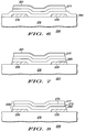
- ballast layer 264 is deposited on column conductor 230 and includes a layer of amorphous silicon which is doped with boron to a concentration of about 10 16 cm -3 of boron. Thereafter, a layer 269 of a diamond-like carbon is deposited onto ballast layer 264. Then, a field shaping layer 274 of amorphous silicon is formed on layer 269.
- layers 264, 269, 274 are patterned to set emissive structure 220 on top of column conductor 230.
- the photoresist employed is a common variety, supplied by Hoechst Celanese, product number AZ5214, for which a suitable etchant includes an oxygen plasma. As indicated above, oxygen plasma is also an etchant with respect to the diamond like carbon. However, the etch rate of the diamond-like carbon by an oxygen plasma is much greater than that of the photoresist. Therefore, as illustrated if FIG. 6, those portions of the diamond-like carbon which lie outside column conductor 230 are removed well before the photoresist is removed. After etching ballast layer 264, layer 221 of photoresist is removed using an oxygen plasma to produce structure 258, shown in FIG. 8.
- the oxygen plasma simultaneously attacks the exposed edges of the field emission material, thereby forming undercut edge 272 of surface emitter 270, as shown in FIG. 8.
- the dielectric material is deposited on structure 258, it is unable to conform to the uneven edge of emissive structure 220, thereby forming void 295, as illustrated in FIG. 3.
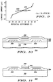
- FIG. 9 there are depicted graphical representation 400, 410 of the row-to-column current leakage exhibited by a field emission device fabricated in the manner described with reference to FIG. 2.
- the current measurements were made in the manner described with reference to FIG. 3, while addressing a single pixel, or one row-column intersection, having nine emission wells, each of which were about 4 micrometers in diameter and 1 micrometer deep.
- Graphs 400, 410 comprise measurements taken at different pixels within an array of pixels of the field emission device.
- the leakage current depicted by graph 410 is substantial, having a value of about 20 microamps for a row-column potential difference of 70 volts, which is a commonly used value. This level of leakage current is unacceptable.
- the leakage current at the site represented by graph 400 shows measurable leakage at voltages above 30 volts.
- Structure 354 includes a supporting substrate 310, which may be made from glass, such as borosilicate glass, or silicon. Upon a major surface of supporting substrate 310 is formed a column conductor 330, which is patterned to have a central well region 332. Upon column conductor 330 is deposited a ballast layer 364.
- ballast layer 364 includes a layer of amorphous silicon which is doped to impart a resistivity within the range of 100 ⁇ cm - 10,000 ⁇ cm. This may be achieved by doping the amorphous silicon with boron to a concentration within a range of 10 10 - 10 18 cm -3 , preferably 10 16 cm -3 , by implantation of boron at 30 keV. Other suitable ballasting materials, having resistivities within the aforementioned range, may be used to form ballast layer 364. Thereafter, a layer 369 of diamond-like carbon, having a thickness of about 1000 angstroms, is formed on ballast layer 364. Other field emissive materials may be employed, including field emissive carbon-based materials.
- an amorphous hydrogenated carbon film can be deposited by plasma-enhanced chemical vapor deposition using gas sources such as cyclohexane, n-hexane, and methane.
- gas sources such as cyclohexane, n-hexane, and methane.
- One such method is described by Wang et al. in "Lithography Using Electron Beam Induced Etching of a Carbon Film", J. Vac. Sci. Technol. Sept/Oct 1995, pp. 1984-1987.
- the deposition of diamond films is described in U.S. Patent No.
- the diamond-like carbon is dry etched using an oxygen plasma, thereby forming a surface emitter 370 generally in registration with central well region 332, to realize structure 355 shown in FIG. 11.
- hardmask 368 is first removed from structure 355 (FIG. 11).
- a field shaping layer 374 of amorphous silicon is formed on surface emitter 370 and ballast layer 364.
- Field shaping layer 374 and ballast layer 364 are etched to generally overlie column conductor 330.
- Ballast layer 364 and field shaping layer 374 have nearly equal etch rates with respect to the aforementioned etchants, so that the opposed edges of column conductor 330, the opposed edges of a ballast 365, and the opposed edges of a field shaper layer 377 define opposed smooth, continuous surfaces 371.
- layer 321 of photoresist is removed using an oxygen plasma. During this step, surface emitter 370, including an edge 372, is protected from attack by the etchant.
- This configuration precludes non-uniform etching at surfaces 371.
- Dielectric layer 341 when a dielectric layer 341 is thereafter deposited, it easily conforms to surfaces 371, thereby preventing the formation of crack-forming voids.
- Dielectric layer 341 is deposited to a thickness of about 1 micrometer.
- a conductive layer 351 made from, for example, molybdenum, is then deposited on dielectric layer 341, thereby realizing structure 358.
- an emission well 360 is formed by selectively etching portions of conductive layer 351, dielectric layer 341, and field shaper layer 377, thereby forming a row conductor 350, a dielectric layer 340, and a field shaper 375.
- Emission well 360 generally overlies central well region 332 and is in registration with surface emitter 370, which defines the bottom surface of emission well 360.
- An emissive structure 320 is comprised of field shaper 375, surface emitter 370, and ballast 365.
- FED 300 further includes an anode 380 spaced from row conductor 350 of a cathode 376.
- the operation of FED 300 includes applying appropriate potentials (by using potential sources, not shown) to column conductor 330 and row conductor 350 for extracting electrons from surface emitter 370 and applying a high positive potential at anode 380 for accelerating the extracted electrons toward anode 380.
- An example of a suitable potential configuration includes: column conductor 330 at ground; row conductor 350 at +80 volts; and anode 380 at +4000 volts.
- the ballast layer is made from the field emissive material, the field emissive material having a resistivity within the ballasting range.
- the ballast layer is patterned to form a ballast having opposed edges which are disposed inwardly, toward the central well region, and on the metal portion of the column conductor.
- the field shaping layer covers the opposed edges of the ballast.
- the field shaping layer is then selectively etched to overlie the column conductor and to form, in conjunction with the opposed edges of the column conductor, smooth surfaces to which the dielectric layer can conform.
- the emissive material is thereby protected during the step of patterning the field shaping layer.
- the emission well is formed by selectively etching through the dielectric and the field shaper layer, to expose a portion of the emissive material of the ballast, thereby providing the surface emitter.
- FIGs. 16 and 17 there are depicted a cross-sectional view (FIG. 16) of a pixel of a field emission device 800, which was made by a method for fabricating a field emission device having reduced row-to-column leakage, in accordance with the present invention, and a top plan view (FIG. 17) of a pixel of a cathode 876 of field emission device 800 of FIG. 16.
- Field emission device 800 was made in the manner described with reference to FIGs. 10 - 15, and elements are similarly referenced, beginning with an "8".
- a column conductor 830 includes three central well portions 832, over which are formed three emission wells 860, each having a surface emitter 870 disposed therein.
- Each of the pixels of field emission device 800 included nine emission wells 860 at each overlapping region between a row conductor 850 and column conductor 830.
- Field emission device 800 included an array of 32x32 row and column conductors, defining 1024 pixels such as depicted in FIGs. 16 and 17.
- FIG. 18 there are depicted graphical representations 700, 710 of row-to-column current leakage currents (in microamperes) exhibited by the 1024 pixels of cathode 876 of field emission device 800 (FIGs. 16 and 17).
- the leakage current measurements were made in the manner described with reference to FIG. 3.
- Graphs 700, 710 comprise measurements taken from two identically configured arrays which were separately fabricated. These measurements include the leakage current contributions of about 1000 times more pixels than those depicted in FIG. 9.
- Graph 700 shows no measurable leakage current for all voltages; graph 710 shows a leakage current of about 7 microamperes at a potential difference of 50 volts, or about 7 nanoamperes per pixel.
- Field emission device 800 fabricated using a method in accordance with the present invention, has a leakage current which is about three orders of magnitude less than that of a field emission device (FIG. 9) having the pixel configuration shown in FIG. 17 and being fabricated in the manner described with reference to FIGs. 4 - 8.
- a method for fabricating a field emission device in accordance with the present invention is useful in processes which further include additional processing steps, subsequent the deposition of the surface emitter, wherein the additional step(s) introduce a chemistry which would otherwise attack the field emissive material to create an edge of the emissive structure to which the dielectric cannot conform.
- the present method may include other field emissive film compositions which are susceptible to attack by processing steps subsequent the formation of the surface emitter.
- the similar compositions of the field shaper and the ballast ensure nearly equal etch rates of these layers by a given etchant, thereby producing a smooth, continuous edge of the emissive structure. The dielectric layer can then easily conform to the edge of the emissive structure, thereby preventing the formation of voids.
Landscapes
- Engineering & Computer Science (AREA)
- Manufacturing & Machinery (AREA)
- Cold Cathode And The Manufacture (AREA)
- Cathode-Ray Tubes And Fluorescent Screens For Display (AREA)
Applications Claiming Priority (2)
| Application Number | Priority Date | Filing Date | Title |
|---|---|---|---|
| US767246 | 1996-12-13 | ||
| US08/767,246 US5696385A (en) | 1996-12-13 | 1996-12-13 | Field emission device having reduced row-to-column leakage |
Publications (3)
| Publication Number | Publication Date |
|---|---|
| EP0848406A2 true EP0848406A2 (fr) | 1998-06-17 |
| EP0848406A3 EP0848406A3 (fr) | 1998-08-12 |
| EP0848406B1 EP0848406B1 (fr) | 2002-07-31 |
Family
ID=25078929
Family Applications (1)
| Application Number | Title | Priority Date | Filing Date |
|---|---|---|---|
| EP97120736A Expired - Lifetime EP0848406B1 (fr) | 1996-12-13 | 1997-11-26 | Dispositif d'émission de champ ayant de fuites réduites entre lignes et colonnes et procédé de sa fabrication |
Country Status (7)
| Country | Link |
|---|---|
| US (2) | US5696385A (fr) |
| EP (1) | EP0848406B1 (fr) |
| JP (1) | JP3954710B2 (fr) |
| KR (1) | KR100441184B1 (fr) |
| CN (1) | CN1155979C (fr) |
| DE (1) | DE69714392T2 (fr) |
| TW (1) | TW358955B (fr) |
Cited By (1)
| Publication number | Priority date | Publication date | Assignee | Title |
|---|---|---|---|---|
| WO2000046834A1 (fr) * | 1999-02-05 | 2000-08-10 | Motorola Inc. | Dispositif a emission de champ pourvu de couches dielectriques de focalisation |
Families Citing this family (23)
| Publication number | Priority date | Publication date | Assignee | Title |
|---|---|---|---|---|
| US5908699A (en) * | 1996-10-11 | 1999-06-01 | Skion Corporation | Cold cathode electron emitter and display structure |
| US7070651B1 (en) * | 1997-05-21 | 2006-07-04 | Si Diamond Technology, Inc. | Process for growing a carbon film |
| US6310432B1 (en) * | 1997-05-21 | 2001-10-30 | Si Diamond Technology, Inc. | Surface treatment process used in growing a carbon film |
| US6181056B1 (en) * | 1997-10-21 | 2001-01-30 | Si Diamond Technology, Inc. | Cold cathode carbon film |
| GB2330687B (en) * | 1997-10-22 | 1999-09-29 | Printable Field Emitters Ltd | Field emission devices |
| US6017772A (en) | 1999-03-01 | 2000-01-25 | Micron Technology, Inc. | Field emission arrays and method of fabricating emitter tips and corresponding resistors thereof with a single mask |
| US6197607B1 (en) | 1999-03-01 | 2001-03-06 | Micron Technology, Inc. | Method of fabricating field emission arrays to optimize the size of grid openings and to minimize the occurrence of electrical shorts |
| US6059625A (en) | 1999-03-01 | 2000-05-09 | Micron Technology, Inc. | Method of fabricating field emission arrays employing a hard mask to define column lines |
| US6359383B1 (en) * | 1999-08-19 | 2002-03-19 | Industrial Technology Research Institute | Field emission display device equipped with nanotube emitters and method for fabricating |
| JP3874396B2 (ja) | 2000-01-13 | 2007-01-31 | パイオニア株式会社 | 電子放出素子及びその製造方法並びに電子放出素子を用いた表示装置 |
| US6753544B2 (en) | 2001-04-30 | 2004-06-22 | Hewlett-Packard Development Company, L.P. | Silicon-based dielectric tunneling emitter |
| US6911768B2 (en) * | 2001-04-30 | 2005-06-28 | Hewlett-Packard Development Company, L.P. | Tunneling emitter with nanohole openings |
| US6542397B2 (en) | 2001-06-25 | 2003-04-01 | Lucent Technologies Inc. | Read only memory structure |
| US6458676B1 (en) | 2001-06-25 | 2002-10-01 | Lucent Technologies Inc. | Method of varying the resistance along a conductive layer |
| US20030073302A1 (en) * | 2001-10-12 | 2003-04-17 | Reflectivity, Inc., A California Corporation | Methods for formation of air gap interconnects |
| US6558968B1 (en) * | 2001-10-31 | 2003-05-06 | Hewlett-Packard Development Company | Method of making an emitter with variable density photoresist layer |
| KR100474271B1 (ko) * | 2002-08-16 | 2005-03-10 | 엘지전자 주식회사 | 전계방출소자 및 그 제조방법 |
| KR100474272B1 (ko) * | 2002-08-16 | 2005-03-10 | 엘지전자 주식회사 | 평면형 전계방출소자 및 그 제조방법 |
| KR20050096534A (ko) * | 2004-03-31 | 2005-10-06 | 삼성에스디아이 주식회사 | 전자 방출 표시 장치의 캐소드 기판 및 그 제조 방법 |
| KR20050113045A (ko) * | 2004-05-28 | 2005-12-01 | 삼성에스디아이 주식회사 | 유기 전계 발광 표시 소자 및 그 제조방법 |
| US7429820B2 (en) * | 2004-12-07 | 2008-09-30 | Motorola, Inc. | Field emission display with electron trajectory field shaping |
| TWI329882B (en) * | 2005-08-25 | 2010-09-01 | Ind Tech Res Inst | Method of fabricating field emission display device and cathode plate thereof |
| US9907020B2 (en) | 2014-06-10 | 2018-02-27 | Hewlett Packard Enterprise Development Lp | Wake up message transmission rate |
Family Cites Families (8)
| Publication number | Priority date | Publication date | Assignee | Title |
|---|---|---|---|---|
| US4040080A (en) * | 1976-03-22 | 1977-08-02 | Hamamatsu Terebi Kabushiki Kaisha | Semiconductor cold electron emission device |
| JP2503621B2 (ja) * | 1989-01-23 | 1996-06-05 | 日本電気株式会社 | 半導体装置の製造方法 |
| US5144191A (en) * | 1991-06-12 | 1992-09-01 | Mcnc | Horizontal microelectronic field emission devices |
| US5397428A (en) * | 1991-12-20 | 1995-03-14 | The University Of North Carolina At Chapel Hill | Nucleation enhancement for chemical vapor deposition of diamond |
| US5473218A (en) * | 1994-05-31 | 1995-12-05 | Motorola, Inc. | Diamond cold cathode using patterned metal for electron emission control |
| DE69513581T2 (de) * | 1994-08-01 | 2000-09-07 | Motorola, Inc. | Bogen-Unterdrückungsvorrichtung für eine Feldemissionsvorrichtung |
| US5826160A (en) * | 1995-08-14 | 1998-10-20 | The United States Of America As Represented By The Secretary Of The Army | Hot explosive consolidation of refractory metal and alloys |
| US5719406A (en) * | 1996-10-08 | 1998-02-17 | Motorola, Inc. | Field emission device having a charge bleed-off barrier |
-
1996
- 1996-12-13 US US08/767,246 patent/US5696385A/en not_active Expired - Lifetime
-
1997
- 1997-08-18 US US08/912,612 patent/US5821132A/en not_active Expired - Fee Related
- 1997-10-24 KR KR1019970054933A patent/KR100441184B1/ko not_active Expired - Fee Related
- 1997-11-08 TW TW086116687A patent/TW358955B/zh not_active IP Right Cessation
- 1997-11-26 DE DE69714392T patent/DE69714392T2/de not_active Expired - Fee Related
- 1997-11-26 EP EP97120736A patent/EP0848406B1/fr not_active Expired - Lifetime
- 1997-12-10 JP JP36191997A patent/JP3954710B2/ja not_active Expired - Fee Related
- 1997-12-11 CN CNB971254540A patent/CN1155979C/zh not_active Expired - Fee Related
Cited By (2)
| Publication number | Priority date | Publication date | Assignee | Title |
|---|---|---|---|---|
| WO2000046834A1 (fr) * | 1999-02-05 | 2000-08-10 | Motorola Inc. | Dispositif a emission de champ pourvu de couches dielectriques de focalisation |
| US6204597B1 (en) | 1999-02-05 | 2001-03-20 | Motorola, Inc. | Field emission device having dielectric focusing layers |
Also Published As
| Publication number | Publication date |
|---|---|
| EP0848406B1 (fr) | 2002-07-31 |
| US5696385A (en) | 1997-12-09 |
| DE69714392T2 (de) | 2003-01-16 |
| DE69714392D1 (de) | 2002-09-05 |
| KR19980063544A (ko) | 1998-10-07 |
| KR100441184B1 (ko) | 2004-12-29 |
| CN1193834A (zh) | 1998-09-23 |
| JP3954710B2 (ja) | 2007-08-08 |
| CN1155979C (zh) | 2004-06-30 |
| TW358955B (en) | 1999-05-21 |
| US5821132A (en) | 1998-10-13 |
| EP0848406A3 (fr) | 1998-08-12 |
| JPH10177838A (ja) | 1998-06-30 |
Similar Documents
| Publication | Publication Date | Title |
|---|---|---|
| EP0848406B1 (fr) | Dispositif d'émission de champ ayant de fuites réduites entre lignes et colonnes et procédé de sa fabrication | |
| US5445550A (en) | Lateral field emitter device and method of manufacturing same | |
| US6144144A (en) | Patterned resistor suitable for electron-emitting device | |
| CA2034481C (fr) | Methode a auto-alignement pour la fabrication d'electrodes de reseaux d'emetteurs | |
| US5396150A (en) | Single tip redundancy method and resulting flat panel display | |
| EP0985220B1 (fr) | Fabrication de dispositif emetteur d'electrons dote d'une electrode d'emission de type echelle | |
| EP0513777A2 (fr) | Dispositif à électrode multiple à électrons à émission de champs et procédé de fabrication | |
| US6514422B2 (en) | Simplified etching technique for producing multiple undercut profiles | |
| JP4001460B2 (ja) | 大領域fed装置及び方法 | |
| EP0501785A2 (fr) | Structure pour émettre des électrons et procédé de fabrication | |
| US20050001529A1 (en) | Barrier metal layer for a carbon nanotube flat panel display | |
| KR100343222B1 (ko) | 전계방출표시소자의제조방법 | |
| US5719406A (en) | Field emission device having a charge bleed-off barrier | |
| JP3246137B2 (ja) | 電界放出カソード及び電界放出カソードの製造方法 | |
| US6008062A (en) | Undercutting technique for creating coating in spaced-apart segments | |
| EP0747920A2 (fr) | Emetteurs d'électrons par le bord pour un réseau de dispositifs à émission de champ | |
| US5848925A (en) | Method for fabricating an array of edge electron emitters | |
| US5857884A (en) | Photolithographic technique of emitter tip exposure in FEDS | |
| US5827100A (en) | Method for manufacturing field emission device | |
| JP3052845B2 (ja) | 集束電極を有する電界放出カソードの製造方法 | |
| JP2003517698A (ja) | 電子放出デバイス製造中のspindtタイプカソードの保護方法 | |
| WO2007089991A2 (fr) | Dispositif d'emission de champ | |
| JP3086445B2 (ja) | 電界放出素子の形成方法 | |
| US5836799A (en) | Self-aligned method of micro-machining field emission display microtips | |
| KR100397616B1 (ko) | 전계효과전자방출소자의제조방법 |
Legal Events
| Date | Code | Title | Description |
|---|---|---|---|
| PUAI | Public reference made under article 153(3) epc to a published international application that has entered the european phase |
Free format text: ORIGINAL CODE: 0009012 |
|
| AK | Designated contracting states |
Kind code of ref document: A2 Designated state(s): DE FR GB |
|
| AX | Request for extension of the european patent |
Free format text: AL;LT;LV;MK;RO;SI |
|
| PUAL | Search report despatched |
Free format text: ORIGINAL CODE: 0009013 |
|
| AK | Designated contracting states |
Kind code of ref document: A3 Designated state(s): AT BE CH DE DK ES FI FR GB GR IE IT LI LU MC NL PT SE |
|
| AX | Request for extension of the european patent |
Free format text: AL;LT;LV;MK;RO;SI |
|
| 17P | Request for examination filed |
Effective date: 19990212 |
|
| AKX | Designation fees paid |
Free format text: DE FR GB |
|
| RBV | Designated contracting states (corrected) |
Designated state(s): DE FR GB |
|
| 17Q | First examination report despatched |
Effective date: 20000629 |
|
| RTI1 | Title (correction) |
Free format text: FIELD EMISSION DEVICE HAVING REDUCED ROW-TO-COLUMN LEAKAGE AND METHOD FOR FABRICATING SAME |
|
| GRAG | Despatch of communication of intention to grant |
Free format text: ORIGINAL CODE: EPIDOS AGRA |
|
| GRAG | Despatch of communication of intention to grant |
Free format text: ORIGINAL CODE: EPIDOS AGRA |
|
| GRAH | Despatch of communication of intention to grant a patent |
Free format text: ORIGINAL CODE: EPIDOS IGRA |
|
| GRAH | Despatch of communication of intention to grant a patent |
Free format text: ORIGINAL CODE: EPIDOS IGRA |
|
| GRAA | (expected) grant |
Free format text: ORIGINAL CODE: 0009210 |
|
| AK | Designated contracting states |
Kind code of ref document: B1 Designated state(s): DE FR GB |
|
| REG | Reference to a national code |
Ref country code: GB Ref legal event code: FG4D |
|
| REF | Corresponds to: |
Ref document number: 69714392 Country of ref document: DE Date of ref document: 20020905 |
|
| ET | Fr: translation filed | ||
| PLBE | No opposition filed within time limit |
Free format text: ORIGINAL CODE: 0009261 |
|
| STAA | Information on the status of an ep patent application or granted ep patent |
Free format text: STATUS: NO OPPOSITION FILED WITHIN TIME LIMIT |
|
| 26N | No opposition filed |
Effective date: 20030506 |
|
| PGFP | Annual fee paid to national office [announced via postgrant information from national office to epo] |
Ref country code: GB Payment date: 20051004 Year of fee payment: 9 |
|
| PGFP | Annual fee paid to national office [announced via postgrant information from national office to epo] |
Ref country code: FR Payment date: 20051104 Year of fee payment: 9 |
|
| PGFP | Annual fee paid to national office [announced via postgrant information from national office to epo] |
Ref country code: DE Payment date: 20051130 Year of fee payment: 9 |
|
| PG25 | Lapsed in a contracting state [announced via postgrant information from national office to epo] |
Ref country code: DE Free format text: LAPSE BECAUSE OF NON-PAYMENT OF DUE FEES Effective date: 20070601 |
|
| GBPC | Gb: european patent ceased through non-payment of renewal fee |
Effective date: 20061126 |
|
| REG | Reference to a national code |
Ref country code: FR Ref legal event code: ST Effective date: 20070731 |
|
| PG25 | Lapsed in a contracting state [announced via postgrant information from national office to epo] |
Ref country code: GB Free format text: LAPSE BECAUSE OF NON-PAYMENT OF DUE FEES Effective date: 20061126 |
|
| PG25 | Lapsed in a contracting state [announced via postgrant information from national office to epo] |
Ref country code: FR Free format text: LAPSE BECAUSE OF NON-PAYMENT OF DUE FEES Effective date: 20061130 |