EP0848432A2 - Tandem-Solarzellen von hohem Wirkungsgrad und Funktionsmethode - Google Patents
Tandem-Solarzellen von hohem Wirkungsgrad und Funktionsmethode Download PDFInfo
- Publication number
- EP0848432A2 EP0848432A2 EP97121519A EP97121519A EP0848432A2 EP 0848432 A2 EP0848432 A2 EP 0848432A2 EP 97121519 A EP97121519 A EP 97121519A EP 97121519 A EP97121519 A EP 97121519A EP 0848432 A2 EP0848432 A2 EP 0848432A2
- Authority
- EP
- European Patent Office
- Prior art keywords
- photons
- solar cells
- spectrally selective
- solar
- cell
- Prior art date
- Legal status (The legal status is an assumption and is not a legal conclusion. Google has not performed a legal analysis and makes no representation as to the accuracy of the status listed.)
- Granted
Links
Images

Classifications
-
- H—ELECTRICITY
- H10—SEMICONDUCTOR DEVICES; ELECTRIC SOLID-STATE DEVICES NOT OTHERWISE PROVIDED FOR
- H10F—INORGANIC SEMICONDUCTOR DEVICES SENSITIVE TO INFRARED RADIATION, LIGHT, ELECTROMAGNETIC RADIATION OF SHORTER WAVELENGTH OR CORPUSCULAR RADIATION
- H10F77/00—Constructional details of devices covered by this subclass
- H10F77/30—Coatings
- H10F77/306—Coatings for devices having potential barriers
- H10F77/311—Coatings for devices having potential barriers for photovoltaic cells
-
- H—ELECTRICITY
- H10—SEMICONDUCTOR DEVICES; ELECTRIC SOLID-STATE DEVICES NOT OTHERWISE PROVIDED FOR
- H10F—INORGANIC SEMICONDUCTOR DEVICES SENSITIVE TO INFRARED RADIATION, LIGHT, ELECTROMAGNETIC RADIATION OF SHORTER WAVELENGTH OR CORPUSCULAR RADIATION
- H10F77/00—Constructional details of devices covered by this subclass
- H10F77/40—Optical elements or arrangements
- H10F77/42—Optical elements or arrangements directly associated or integrated with photovoltaic cells, e.g. light-reflecting means or light-concentrating means
- H10F77/488—Reflecting light-concentrating means, e.g. parabolic mirrors or concentrators using total internal reflection
-
- Y—GENERAL TAGGING OF NEW TECHNOLOGICAL DEVELOPMENTS; GENERAL TAGGING OF CROSS-SECTIONAL TECHNOLOGIES SPANNING OVER SEVERAL SECTIONS OF THE IPC; TECHNICAL SUBJECTS COVERED BY FORMER USPC CROSS-REFERENCE ART COLLECTIONS [XRACs] AND DIGESTS
- Y02—TECHNOLOGIES OR APPLICATIONS FOR MITIGATION OR ADAPTATION AGAINST CLIMATE CHANGE
- Y02E—REDUCTION OF GREENHOUSE GAS [GHG] EMISSIONS, RELATED TO ENERGY GENERATION, TRANSMISSION OR DISTRIBUTION
- Y02E10/00—Energy generation through renewable energy sources
- Y02E10/50—Photovoltaic [PV] energy
- Y02E10/52—PV systems with concentrators
Definitions
- This invention relates to solar cells, and more specifically to tandem solar cells that efficiently convert solar radiation into electrical energy.
- Solar cells are photovoltaic devices that use semiconductors to convert photons into electrical energy.
- a conduction band and a valence band are separated by an energy gap E g that varies with material composition and temperature.
- E g energy gap
- a photon is absorbed by a semiconductor, an electron is promoted from the valence band into the conduction band, thereby creating a hole in the valence band. Since a hole represents the absence of an electron, it can be regarded as a positive charge carrier.
- p-n junctions are ideal for converting solar radiation into electricity.
- any extra energy in the proton (h ⁇ - E g ) is converted into thermal rather than electrical energy, since only one electron-hole pair can be created for each absorption event.
- a semiconductor is more transparent to wavelengths corresponding to energies less than E g , since in this case the photons are not energetic enough to promote electrons from the valence band into the conduction band.
- no single semiconducting material can convert the entire solar spectrum into electrical energy, since the most energetic photons produce largely thermal energy and are therefore inefficiently utilized, while the least energetic photons cannot be absorbed.
- tandem solar cells By cascading the p-n junctions of different materials, however, the overall conversion efficiency can be improved.
- a top cell having a p-n junction of a high energy band gap semiconductor intercepts the most energetic photons. Lower energy photons pass through the top cell before they enter another cell having a p-n junction of a lower energy band gap semiconductor. In this way, an additional portion of the solar spectrum is used.
- tunnel junctions are often used to connect p-n junctions, so that current can pass from one cell to the next.
- the various layers must have thermal properties and lattice spacings which are compatible with each other. Otherwise, internal strains will be introduced during the epitaxial growth process, resulting in defects which will then propagate throughout the entire structure.
- tandem solar cell An example of a tandem solar cell is the GaInP/GaAs dual junction cell grown on a GaAs substrate, which is described by S. Kurtz et al. in "19.6% Electron-Irradiated GaInP/GaAs Cells," Proceedings of 1st WCPEC (World Conference on Photovoltaic Energy Conversion), pp. 2108-2111, 1994.
- This tandem solar cell produced 19.6% conversion efficiency of the air mass zero (AM0) solar spectrum, which is the pure solar spectrum with no atmospheric absorption.
- GaInP/GaAs cells have also been grown on Ge substrates, as reported by P.K.
- GaInAsP and GaInAs individually are better converters of the IR than Ge, as indicated by M.W. Wanlass et al. in "Development of High-Performance GaInAsP Solar Cells for Tandem Solar Cell Applications," Proceedings of the 21st IEEE Photovoltaic Specialists Conference, pp. 172-178, 1990.
- GaInAsP and GaInAs have lattice spacings bite different from Ge, so that it is not possible to construct a monolithic structure by simply epitaxially depositing one layer on top of another.
- Semiconductors having different lattice structures can be connected, however, by using transparent adhesive layers to connect semiconductor layers both mechanically and optically. (See, for example, J.C.C.
- a photovoltaic device which optically joins different semiconductor layers without using a transparent adhesive layer is described in U.S. Patent 4,328,389 to Stern et al.
- a first broadband reflector concentrates sunlight on a high energy band gap photovoltaic array that converts high energy photons into electricity.
- a second broadband reflector is positioned behind the first array and reflects and concentrates light that is not absorbed in the first array back through it towards a second photovoltaic array which has a low energy band gap and converts low energy photons into electricity.
- low energy photons must pass through the first array twice before they reach the second array, resulting in absorption losses which can be significant if the density of free carriers in the first array is high.
- the device of Stern et al. is only designed for use with solar concentrator systems and specifically avoids spectrally selective reflectors.
- the present invention is a high efficiency photovoltaic device in which photons are directed towards different solar cells depending upon their wavelength. Absorption losses are reduced since photons are imaged towards those semiconductor layers that convert them into electricity.
- the invention includes preferably two solar cells which have different effective band gaps and are designed to efficiently convert either high or low energy photons into electricity.
- a spectrally selective reflector is placed between incoming photons and one of the two solar cells, designated as the first solar cell, and is preferably applied directly as a coating to the first solar cell or to a layer of substantially transparent glass which is joined to the first solar cell by an adhesive.
- the spectrally selective reflector transmits photons with the proper energy into the first solar cell, while reflecting photons that can be efficiently converted by the second solar cell towards that cell. In this way, high and low energy photons are imaged directly towards solar cells having high and low energy effective band gaps, respectively.
- One advantage of the invention is that it allows low cost substrates to be used, since a single monolithic structure incorporating both high and low energy band gap materials is not required.
- Ge can be used as the substrate for a high energy band gap GaInP/GaAs cell rather than costly low doped GaAs, which would otherwise be required in a stacked approach to reduce IR absorption.
- GaInAsP or GaInAsP/GaInAs can be used as the low band gap material, with InP used as the substrate.
- Ge or Si may also be used in a "lattice mismatched" configuration.
- the solar cells and the spectrally selective reflector are combined with a substantially flat broadband mirror that faces the radiation source and images incoming photons towards the spectrally selective reflector.
- This configuration allows for greater radiation shielding of the invention, which is important in space where solar cells can encounter a variety of high energy particles that cause degradation in power output over the operating life of a satellite.
- the modular design of the invention allows it to be compactly stowed for launch and then deployed in space.
- the invention may be integrated in either space or on the ground with a solar concentrator system for focusing solar radiation.
- the present invention is a photovoltaic device that uses a spectrally selective photon partitioner such as a spectrally selective reflector for imaging photons towards different solar cells, depending upon their energy.
- Photon partitioners other than spectrally selective reflectors can be used to separate photons by energy (such as prisms and diffraction gratings), with solar cells being positioned to receive light accordingly.
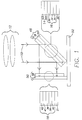
- Incident sunlight, or more generally, photons are represented in FIG. 1 by incoming light rays 10. The term light is used broadly herein to encompass both visible and invisible electromagnetic radiation.
- a solar concentrator system 12 is represented schematically by lenses and can be used to collect sunlight from a wide area and direct it (collimate and/or focus it) towards a spectrally selective reflector 14 that overlies a solar cell 16.
- solar concentrators extend over a much wider area than the solar cells to which they image light.
- the spectrally selective reflector 14 is oriented preferably at 45 degrees to the sun and transmits those photons that can be converted into electricity by solar cell 16 while reflecting other photons towards another solar cell 18.
- Solar cells 16 and 18 overlie respective backplates 20 and 21 and can be individually sized and series connected to build desired cell circuits.
- solar cells 16 and 18 have high and low effective band gaps, respectively, then solar cell 16 will efficiently convert high energy photons while solar cell 18 efficiently converts low energy photons.
- the spectrally selective reflector 14 transmits high energy photons into solar cell 16 while reflecting low energy photons towards solar cell 18.
- solar cells 16 and 18 can be designed for low and high energy photons, respectively, in which case the spectrally selective reflector 14 transmits low energy photons while reflecting high energy photons towards solar cell 18.
- the spectrally selective reflector 14 partitions photons such that photons with energies lying between the effective band gaps of solar cells 16 and 18 are imaged towards that solar cell that has the smaller effective band gap, whereas photons that are more energetic than either of the two band gaps are imaged towards that cell having the larger effective band gap.
- This partitioning of the photons efficiently converts the energy of the photons into electricity. Where photons with energies below the band gaps of both cells are imaged is not of immediate interest, since they cannot be converted into electricity in either cell.
- Solar cells 16 and 18 may comprise a variety of materials formed by different techniques including molecular beam epitaxy and diffusion. Cutaways in FIG. 1 show in greater detail how solar cells 16 and 18, spectrally selective reflector 14 and backplates 20 and 21 are preferably constructed and their relationship to each other. Solar cell 16 is shown here as the high energy band gap cell which preferably comprises 5 micron thick layers of GaInP 30 and GaAs 32 grown on a substrate 34 that is preferably 170 micron thick Ge.
- GaInP and GaAs have band gaps of 1.85 eV and 1.45 eV, respectively, photons having wavelengths (as measured in vacuum) shorter than 0.67 microns are absorbed in the GaInP layer 30, whereas the GaAs layer 32 will produce electricity from photons passing through the GaInP layer 30 which have wavelengths between 0.67 and 0.89 microns.
- solar cell 16 has an effective band gap defined by the GaAs layer 32, i.e. 1.45 eV, so that solar cell 16 converts photons having vacuum wavelengths less than 0.89 microns.
- the low energy band gap cell is shown here as solar cell 18 and preferably includes 3-5 micron thick layers of GaInAsP 36 and alternatively GaInAs 38 as well grown on a substrate 40 that is preferably 350 micron thick InP.
- GaInAsP and GaInAs have band gaps of 1.03 and 0.74 eV, respectively, so that cell 18 has an effective band gap of 0.74 eV. That is, photons having wavelengths less than 1.3 microns will be absorbed in the GaInAsP layer 36, whereas the GaInAs layer 38 will produce electricity only from photons falling in the wavelength range between 1.3 and 1.7 microns.
- Photons having wavelengths longer than 1.7 microns cannot produce electron-hole pairs in GaInAs, since they are not energetic enough to promote an electron from the conduction band to the valence band.
- Other semiconductor materials can be used as low band gap materials, such as GaSb, Si, CuInGaSe and GaAs, whereas substrate 40 may also comprise materials such as Si or Ge.
- a substantially transparent glass layer 41 can be placed on top of the active semiconductor materials of solar cell 18 (or cell 16) to protect it from cosmic radiation.
- An anti-reflection coating 42 for reducing infrared reflection may be applied to one or both sides of glass layer 41 or, when glass layer 41 is not used, directly onto the GaInAsP layer 36.
- the spectrally selective reflector 14 is designed to generally transmit photons having wavelengths less than 0.89 microns into solar cell 16, but generally reflect photons between 0.89 and 1.7 microns towards solar cell 18.
- the spectrally selective reflector 14 preferably includes a spectrally selective coating 43 applied to a substantially transparent glass layer 44 that in turn is bonded to the solar cell 16 with an optically transparent adhesive such as Dow Corning Inc. type 93-500.
- Coating 43 may also be applied directly to solar cell 16, however, and may be a multilayer coating comprising a series of TiO 2 and SiO 2 layers. Alternatively, it may be a single layer with a spatially varying refractive index.
- the spectrally selective reflector 14 permits photons to be more directly imaged towards those semiconductor layers in which they generate electricity than do tandem cells in which transparent adhesive layers are used to join the semiconductor layers. This approach substantially reduces absorption of the incident sunlight by free carriers, thereby increasing the overall solar to electrical energy conversion efficiency. Furthermore, it permits low cost Ge to be used as the substrate 34 for the GaInP and GaAs layers 30 and 32, rather than the more expensive GaAs, which would otherwise be required because of its better transmission properties in the infrared.
- Backplates 20 and 21 provide a mechanical platform for solar cells 16 and 18.
- the backplates 20 and 21 are preferably 250-500 micron thick graphite epoxy or metal such as copper, since these materials are relatively light-weight, rigid, and are effective absorbers of cosmic radiation.
- Solar cell 16, spectrally selective reflector 14 and backplate 20 form a solar panel 48
- solar cell 18 and backplate 21 form a solar panel 50.
- the solar panels 48 and 50 can be mounted with hinges, brackets or other support structures (not shown in FIG. 1) to a facesheet 52 that is preferably 100-500 micron thick KevlarTM or aluminum.
- the facesheet 52 can in turn be secured, for example, to an aluminum honeycomb structure like that commonly used to support solar panels in space.
- panel 50 could include a spectrally selective reflector that reflects light between 1.3 and 1.7 microns while transmitting light between 0.89 and 1.3 microns.
- GaInAs layer 38 would not be part of panel 50 but would form its own panel, and panel 50 would be oriented so that light between 1.3 and 1.7 microns would be reflected onto this GaInAs-containing panel.
- FIG. 2 shows an array of pairs of solar panels 48 and 50, in which each pair of panels is used in conjunction with a mirror 60 that is preferably oriented at 45 degrees to incident sunlight.
- the mirrors 60 are preferably substantially flat, broadband reflectors that reflect those photons that can be converted into electricity.
- Aluminized Mylar bonded to a supporting medium or polished aluminum by itself can be used for this purpose.
- An optional solar concentrator system 12' is represented schematically by lenses and can be used to collect sunlight from a wide area and direct it (collimate and/or focus it) towards the mirrors 60.
- System 12' preferably extends over a much larger area than that represented by the panels 48 and 50.
- Light rays 10' are reflected by mirrors 60 towards solar panels 48, which include solar cells 16 and spectrally selective reflectors 14, as shown in FIG. 1.
- the spectrally selective reflectors 14 redirect those photons that can be efficiently converted by solar cells 18 towards solar panels 50.
- Solar panels 48 and 50 and mirrors 60 are preferably arranged in a close packing configuration as shown in FIG. 2, in which panels 48 and mirrors 60 adjoin but face away from each other, and have approximately the same length.
- Solar panels 50 are preferably oriented perpendicular to light rays 10', and collect the photon flux reflected from the spectrally selective reflectors 14. As in FIG.
- a facesheet 53 (that is like its counterpart 52) can be used to support solar panels 48 and 50 and mirrors 60.
- hinges (not shown) between the facesheet 53 and each solar panel 48/mirror 60 pair, the solar panels 48 and mirrors 60 can be permitted to rest on the solar panels 50 during storage, and then raised prior to use with tensioning cords (not shown) that are also attached to the facesheet 53 and the solar panels 48 and mirrors 60.
- tensioning cords not shown
- An advantage of the configuration illustrated in FIG. 2 is that the solar cells can be better shielded from cosmic radiation that would otherwise damage them.
- cosmic radiation emanating from the sun must pass through one of the mirrors 60 as well as one of the backplates 20 and one of the substrates 34 in solar panel 48 (shown in FIG. 1) before reaching active semiconductor layers.
- glass layers such as layer 41 can still be used if desired to shield the active semiconductor layers of solar cells 16 and 18 from cosmic radiation that propagates at an oblique angle with respect to light rays 10'.
Landscapes
- Photovoltaic Devices (AREA)
Applications Claiming Priority (2)
| Application Number | Priority Date | Filing Date | Title |
|---|---|---|---|
| US764803 | 1996-12-12 | ||
| US08/764,803 US5902417A (en) | 1996-12-12 | 1996-12-12 | High efficiency tandem solar cells, and operating method |
Publications (3)
| Publication Number | Publication Date |
|---|---|
| EP0848432A2 true EP0848432A2 (de) | 1998-06-17 |
| EP0848432A3 EP0848432A3 (de) | 1998-12-30 |
| EP0848432B1 EP0848432B1 (de) | 2009-09-16 |
Family
ID=25071833
Family Applications (1)
| Application Number | Title | Priority Date | Filing Date |
|---|---|---|---|
| EP97121519A Expired - Lifetime EP0848432B1 (de) | 1996-12-12 | 1997-12-06 | Tandem-Solarzellen von hohem Wirkungsgrad |
Country Status (3)
| Country | Link |
|---|---|
| US (1) | US5902417A (de) |
| EP (1) | EP0848432B1 (de) |
| DE (1) | DE69739578D1 (de) |
Cited By (6)
| Publication number | Priority date | Publication date | Assignee | Title |
|---|---|---|---|---|
| WO2005050744A3 (en) * | 2003-11-14 | 2005-11-17 | Boeing Co | Improved solar power collection with near infrared wideband reflector coating |
| WO2007095892A3 (de) * | 2006-02-22 | 2007-11-01 | Durlum Leuchten | Konzentrierende solarkollektoren mit dünnschichtzellen |
| WO2008145176A1 (en) * | 2007-05-28 | 2008-12-04 | Consiglio Nazionale Delle Ricerche - Infm Istituto Nazionale Per La Fisica Della Materia | Photovoltaic device with enhanced light harvesting |
| ITPD20080259A1 (it) * | 2008-09-10 | 2010-03-11 | Dichroic Cell Srl | Dispositivo fotovoltaico con ricoprimento superficiale dicroico integrato |
| US8928988B1 (en) | 2011-04-01 | 2015-01-06 | The Regents Of The University Of California | Monocentric imaging |
| US9274266B2 (en) | 2008-09-19 | 2016-03-01 | The Regents Of The University Of California | System and method for solar energy capture and related method of manufacturing |
Families Citing this family (37)
| Publication number | Priority date | Publication date | Assignee | Title |
|---|---|---|---|---|
| US6469241B1 (en) * | 2001-06-21 | 2002-10-22 | The Aerospace Corporation | High concentration spectrum splitting solar collector |
| GB0118150D0 (en) * | 2001-07-25 | 2001-09-19 | Imperial College | Thermophotovoltaic device |
| US6660928B1 (en) | 2002-04-02 | 2003-12-09 | Essential Research, Inc. | Multi-junction photovoltaic cell |
| US6689949B2 (en) * | 2002-05-17 | 2004-02-10 | United Innovations, Inc. | Concentrating photovoltaic cavity converters for extreme solar-to-electric conversion efficiencies |
| US7619159B1 (en) * | 2002-05-17 | 2009-11-17 | Ugur Ortabasi | Integrating sphere photovoltaic receiver (powersphere) for laser light to electric power conversion |
| JP3902109B2 (ja) * | 2002-10-02 | 2007-04-04 | 本田技研工業株式会社 | 赤外線カメラ特性確認治具 |
| US20050247339A1 (en) * | 2004-05-10 | 2005-11-10 | Imperial College Innovations Limited | Method of operating a solar cell |
| WO2006119305A2 (en) * | 2005-05-03 | 2006-11-09 | University Of Delaware | Ultra and very-high efficiency solar cells |
| GB0519599D0 (en) * | 2005-09-26 | 2005-11-02 | Imp College Innovations Ltd | Photovoltaic cells |
| US7158306B1 (en) * | 2005-11-30 | 2007-01-02 | Corning Incorporated | Light separator |
| US7741557B2 (en) * | 2005-12-19 | 2010-06-22 | Corning Incorporated | Apparatus for obtaining radiant energy |
| US20070277869A1 (en) * | 2006-04-27 | 2007-12-06 | Intematix Corporation | Systems and methods for enhanced solar module conversion efficiency |
| JP2009545184A (ja) * | 2006-07-28 | 2009-12-17 | ユニバーシティー、オブ、デラウェア | 周囲のシリコンスカベンジャーセルを備えた高効率太陽電池 |
| KR20090117691A (ko) * | 2006-07-28 | 2009-11-12 | 유니버시티 오브 델라웨어 | 고효율 태양 전지 |
| US20080216885A1 (en) * | 2007-03-06 | 2008-09-11 | Sergey Frolov | Spectrally adaptive multijunction photovoltaic thin film device and method of producing same |
| EP2183790A2 (de) * | 2007-08-29 | 2010-05-12 | University Of Delaware | Hybrid-solarzelle mit hohem wirkungsgrad |
| US20100078063A1 (en) * | 2007-08-29 | 2010-04-01 | Barnett Allen M | High efficiency hybrid solar cell |
| US8487179B2 (en) * | 2008-02-07 | 2013-07-16 | Rebecca Grace Willmott | System and method for the improvement of photovoltaic cell efficiency |
| US20090211622A1 (en) * | 2008-02-21 | 2009-08-27 | Sunlight Photonics Inc. | Multi-layered electro-optic devices |
| US10211353B2 (en) * | 2008-04-14 | 2019-02-19 | Sunlight Photonics Inc. | Aligned bifacial solar modules |
| GB2459651A (en) * | 2008-04-28 | 2009-11-04 | Quantasol Ltd | Concentrator photovoltaic cell |
| TWI381141B (zh) * | 2008-08-13 | 2013-01-01 | Sunplus Mmedia Inc | 太陽能系統 |
| WO2010124204A2 (en) * | 2009-04-24 | 2010-10-28 | Light Prescriptions Innovators, Llc | Photovoltaic device |
| US20100300892A1 (en) * | 2009-06-02 | 2010-12-02 | Herbert Franz Matare | Apparatus and Method for Solar Hydrogen Synfuel Production |
| EP2504863B1 (de) * | 2009-11-24 | 2021-01-13 | Guy Pizzarello | Niedrigprofil-sonnenverfolgungssysteme und -verfahren |
| US20120007434A1 (en) * | 2010-02-04 | 2012-01-12 | Massachusetts Institute Of Technology | Three-dimensional photovoltaic apparatus and method |
| WO2011097585A1 (en) * | 2010-02-05 | 2011-08-11 | Energy Focus, Inc. | Method of making an arrangement for collecting or emitting light |
| US9893223B2 (en) | 2010-11-16 | 2018-02-13 | Suncore Photovoltaics, Inc. | Solar electricity generation system |
| US9559235B2 (en) | 2010-12-17 | 2017-01-31 | Semiconductor Energy Laboratory Co., Ltd. | Photoelectric conversion device |
| US11121272B2 (en) | 2011-02-09 | 2021-09-14 | Utica Leaseco, Llc | Self-bypass diode function for gallium arsenide photovoltaic devices |
| US9716196B2 (en) * | 2011-02-09 | 2017-07-25 | Alta Devices, Inc. | Self-bypass diode function for gallium arsenide photovoltaic devices |
| GB2504977B (en) | 2012-08-16 | 2017-10-04 | Airbus Defence & Space Gmbh | Laser power converter |
| WO2015031135A1 (en) * | 2013-08-27 | 2015-03-05 | Cogenra Solar, Inc. | Split spectrum solar energy collector |
| US10686089B2 (en) * | 2014-11-25 | 2020-06-16 | Ricoh Company, Ltd. | Concentrator photovoltaic cell |
| WO2016148668A2 (en) * | 2015-03-16 | 2016-09-22 | T. C. Marmara Universitesi | A solar energy system allowing the spread of the unit of light beam to a larger receiver surface in the same unit area |
| FR3074964B1 (fr) * | 2017-12-07 | 2019-11-29 | Commissariat A L'energie Atomique Et Aux Energies Alternatives | Fabrication d'un sous-module a concentration utilisant les procedes d'assemblage du photovoltaique |
| US20230057141A1 (en) * | 2021-08-23 | 2023-02-23 | Yonghua Wang | Inflatable Non-Imaging concentrator photonic crystal solar spectrum splitter perovskite integrated circuit concentrating photovoltaic system |
Citations (1)
| Publication number | Priority date | Publication date | Assignee | Title |
|---|---|---|---|---|
| US4328389A (en) | 1981-02-19 | 1982-05-04 | General Dynamics Corporation | Inherent spectrum-splitting photovoltaic concentrator system |
Family Cites Families (2)
| Publication number | Priority date | Publication date | Assignee | Title |
|---|---|---|---|---|
| JPS6159884A (ja) * | 1984-08-31 | 1986-03-27 | Nec Corp | 太陽電池モジユ−ル |
| JPH0463320A (ja) * | 1989-03-08 | 1992-02-28 | Victor Co Of Japan Ltd | 光―光変換素子 |
-
1996
- 1996-12-12 US US08/764,803 patent/US5902417A/en not_active Expired - Lifetime
-
1997
- 1997-12-06 EP EP97121519A patent/EP0848432B1/de not_active Expired - Lifetime
- 1997-12-06 DE DE69739578T patent/DE69739578D1/de not_active Expired - Lifetime
Patent Citations (1)
| Publication number | Priority date | Publication date | Assignee | Title |
|---|---|---|---|---|
| US4328389A (en) | 1981-02-19 | 1982-05-04 | General Dynamics Corporation | Inherent spectrum-splitting photovoltaic concentrator system |
Non-Patent Citations (6)
| Title |
|---|
| BEAUMONT, B. ET AL.: "A Four-Cell Photovoltaic System Based on InP and GaAs", 16TH LE.E.E. PHOTOVOLTAIC SPECIALISTS, SEPTEMBER, 1982, pages 595 - 600, XP002082165 |
| DAVIES ET AL.: "Calculations of efficiencies achievable using gallium arsenide and silicon cells mounted together in cavities illuminated by single-stage concentration", SOLAR ENERGY MATERIALS AND SOLAR CELLS, vol. 26, 1992, pages 203 - 215, XP000274201, DOI: doi:10.1016/0927-0248(92)90061-S |
| J.C.C. FAN ET AL.: "Optimal Design of High-Efficiency Tandem Cells", PROCEEDINGS OF THE 16TH IEEE PHOTOVOLTAIC SPECIALISTS CONFERENCE, 1982, pages 692 - 704 |
| M.W. WANLASS ET AL.: "Development of High-Performance GaInAsP Solar Cells for Tandem Solar Cell Applications", PROCEEDINGS OF THE 21ST IEEE PHOTOVOLTAIC SPECIALISTS CONFERENCE, 1990, pages 172 - 178 |
| P.K. CHIANG: "Large Area GaInp2/GaAs/Ge Multijunction Solar Cells for Space Applications", PROCEEDINGS OF LST WCPEC, 1994, pages 2120 - 2123, XP000680195, DOI: doi:10.1109/WCPEC.1994.521640 |
| S. KURTZ ET AL.: "19.6% Electron-Irradiated GaInP/GaAs Cells", PROCEEDINGS OF LST WCPEC (WORLD CONFERENCE ON PHOTOVOLTAIC ENERGY CONVERSION, 1994, pages 2108 - 2111, XP000680194, DOI: doi:10.1109/WCPEC.1994.521637 |
Cited By (7)
| Publication number | Priority date | Publication date | Assignee | Title |
|---|---|---|---|---|
| WO2005050744A3 (en) * | 2003-11-14 | 2005-11-17 | Boeing Co | Improved solar power collection with near infrared wideband reflector coating |
| WO2007095892A3 (de) * | 2006-02-22 | 2007-11-01 | Durlum Leuchten | Konzentrierende solarkollektoren mit dünnschichtzellen |
| WO2008145176A1 (en) * | 2007-05-28 | 2008-12-04 | Consiglio Nazionale Delle Ricerche - Infm Istituto Nazionale Per La Fisica Della Materia | Photovoltaic device with enhanced light harvesting |
| ITPD20080259A1 (it) * | 2008-09-10 | 2010-03-11 | Dichroic Cell Srl | Dispositivo fotovoltaico con ricoprimento superficiale dicroico integrato |
| US9274266B2 (en) | 2008-09-19 | 2016-03-01 | The Regents Of The University Of California | System and method for solar energy capture and related method of manufacturing |
| US8928988B1 (en) | 2011-04-01 | 2015-01-06 | The Regents Of The University Of California | Monocentric imaging |
| US9482850B2 (en) | 2011-04-01 | 2016-11-01 | The Regents Of The University Of California | Monocentric imaging |
Also Published As
| Publication number | Publication date |
|---|---|
| EP0848432B1 (de) | 2009-09-16 |
| EP0848432A3 (de) | 1998-12-30 |
| DE69739578D1 (de) | 2009-10-29 |
| US5902417A (en) | 1999-05-11 |
Similar Documents
| Publication | Publication Date | Title |
|---|---|---|
| US5902417A (en) | High efficiency tandem solar cells, and operating method | |
| US20210151620A1 (en) | Method and means for a high power solar cell | |
| US20090250097A1 (en) | Solar-To-Electricity Conversion System | |
| US20080230112A1 (en) | Photovoltaic cells | |
| KR20090117691A (ko) | 고효율 태양 전지 | |
| EP1872412A2 (de) | Auf spektrale aufteilung basierendes photovoltaisches strahlungskonzentrationssystem | |
| US20070227582A1 (en) | Low aspect ratio concentrator photovoltaic module with improved light transmission and reflective properties | |
| JP2009545184A (ja) | 周囲のシリコンスカベンジャーセルを備えた高効率太陽電池 | |
| US20140174498A1 (en) | Solar energy production system | |
| JP6222667B2 (ja) | 蓄電型ソーラー発電装置及び蓄電型ソーラー発電システム | |
| JP2015530747A (ja) | スペクトル光分割用モジュールおよび集光器光学部品を含んでいる光起電力システム | |
| US7994417B1 (en) | Optimal cell selection for series connection in Cassegrain PV module | |
| Karp et al. | Multiband solar concentrator using transmissive dichroic beamsplitting | |
| WO1987001512A1 (en) | High efficiency photovoltaic assembly | |
| US20200185557A1 (en) | Device for harvesting sunlight | |
| JP2010538455A (ja) | 高効率ハイブリッド太陽電池 | |
| US20100078063A1 (en) | High efficiency hybrid solar cell | |
| US20240291419A1 (en) | Tandem Photovoltaic and Thermophotovoltaic Cell Assemblies for Converting Solar Energy to Electricity and Methods and Systems Therefor | |
| JP2015530746A (ja) | 光捕捉フィルタ付き光学モジュールを含む光起電力システム | |
| JPH1079526A (ja) | 波長分割集光型太陽電池 | |
| US20170012157A1 (en) | Spectral light splitting module and photovoltaic system | |
| Onffroy et al. | High-Efficiency Spectrophotovoltaic System for Orbital Power Generation | |
| JP2009517878A (ja) | 高いスペクトル放射照度用の透過率を低下させた光電変換装置 |
Legal Events
| Date | Code | Title | Description |
|---|---|---|---|
| PUAI | Public reference made under article 153(3) epc to a published international application that has entered the european phase |
Free format text: ORIGINAL CODE: 0009012 |
|
| AK | Designated contracting states |
Kind code of ref document: A2 Designated state(s): DE FR GB IT NL |
|
| AX | Request for extension of the european patent |
Free format text: AL;LT;LV;MK;RO;SI |
|
| PUAL | Search report despatched |
Free format text: ORIGINAL CODE: 0009013 |
|
| AK | Designated contracting states |
Kind code of ref document: A3 Designated state(s): AT BE CH DE DK ES FI FR GB GR IE IT LI LU MC NL PT SE |
|
| AX | Request for extension of the european patent |
Free format text: AL;LT;LV;MK;RO;SI |
|
| RAP1 | Party data changed (applicant data changed or rights of an application transferred) |
Owner name: HUGHES ELECTRONICS CORPORATION |
|
| 17P | Request for examination filed |
Effective date: 19990619 |
|
| AKX | Designation fees paid |
Free format text: DE FR GB IT NL |
|
| 17Q | First examination report despatched |
Effective date: 20051125 |
|
| RTI1 | Title (correction) |
Free format text: HIGH EFFICIENY TANDEM SOLAR CELLS |
|
| GRAP | Despatch of communication of intention to grant a patent |
Free format text: ORIGINAL CODE: EPIDOSNIGR1 |
|
| GRAS | Grant fee paid |
Free format text: ORIGINAL CODE: EPIDOSNIGR3 |
|
| GRAA | (expected) grant |
Free format text: ORIGINAL CODE: 0009210 |
|
| AK | Designated contracting states |
Kind code of ref document: B1 Designated state(s): DE FR GB IT NL |
|
| REG | Reference to a national code |
Ref country code: GB Ref legal event code: FG4D |
|
| REF | Corresponds to: |
Ref document number: 69739578 Country of ref document: DE Date of ref document: 20091029 Kind code of ref document: P |
|
| PG25 | Lapsed in a contracting state [announced via postgrant information from national office to epo] |
Ref country code: NL Free format text: LAPSE BECAUSE OF FAILURE TO SUBMIT A TRANSLATION OF THE DESCRIPTION OR TO PAY THE FEE WITHIN THE PRESCRIBED TIME-LIMIT Effective date: 20090916 |
|
| NLV1 | Nl: lapsed or annulled due to failure to fulfill the requirements of art. 29p and 29m of the patents act | ||
| PLBE | No opposition filed within time limit |
Free format text: ORIGINAL CODE: 0009261 |
|
| STAA | Information on the status of an ep patent application or granted ep patent |
Free format text: STATUS: NO OPPOSITION FILED WITHIN TIME LIMIT |
|
| 26N | No opposition filed |
Effective date: 20100617 |
|
| REG | Reference to a national code |
Ref country code: FR Ref legal event code: PLFP Year of fee payment: 19 |
|
| REG | Reference to a national code |
Ref country code: FR Ref legal event code: PLFP Year of fee payment: 20 |
|
| PG25 | Lapsed in a contracting state [announced via postgrant information from national office to epo] |
Ref country code: IT Free format text: LAPSE BECAUSE OF NON-PAYMENT OF DUE FEES Effective date: 20151206 |
|
| PGFP | Annual fee paid to national office [announced via postgrant information from national office to epo] |
Ref country code: GB Payment date: 20161228 Year of fee payment: 20 |
|
| PGFP | Annual fee paid to national office [announced via postgrant information from national office to epo] |
Ref country code: FR Payment date: 20161227 Year of fee payment: 20 |
|
| PGFP | Annual fee paid to national office [announced via postgrant information from national office to epo] |
Ref country code: DE Payment date: 20161229 Year of fee payment: 20 |
|
| PG25 | Lapsed in a contracting state [announced via postgrant information from national office to epo] |
Ref country code: IT Free format text: LAPSE BECAUSE OF NON-PAYMENT OF DUE FEES Effective date: 20151206 |
|
| PGFP | Annual fee paid to national office [announced via postgrant information from national office to epo] |
Ref country code: IT Payment date: 20161222 Year of fee payment: 20 |
|
| PGRI | Patent reinstated in contracting state [announced from national office to epo] |
Ref country code: IT Effective date: 20170710 |
|
| REG | Reference to a national code |
Ref country code: DE Ref legal event code: R071 Ref document number: 69739578 Country of ref document: DE |
|
| REG | Reference to a national code |
Ref country code: GB Ref legal event code: PE20 Expiry date: 20171205 |
|
| PG25 | Lapsed in a contracting state [announced via postgrant information from national office to epo] |
Ref country code: GB Free format text: LAPSE BECAUSE OF EXPIRATION OF PROTECTION Effective date: 20171205 |