EP0848583A1 - Dispositif d'affichage - Google Patents
Dispositif d'affichage Download PDFInfo
- Publication number
- EP0848583A1 EP0848583A1 EP97117125A EP97117125A EP0848583A1 EP 0848583 A1 EP0848583 A1 EP 0848583A1 EP 97117125 A EP97117125 A EP 97117125A EP 97117125 A EP97117125 A EP 97117125A EP 0848583 A1 EP0848583 A1 EP 0848583A1
- Authority
- EP
- European Patent Office
- Prior art keywords
- substrate
- display device
- perforation
- strips
- starting substrate
- Prior art date
- Legal status (The legal status is an assumption and is not a legal conclusion. Google has not performed a legal analysis and makes no representation as to the accuracy of the status listed.)
- Granted
Links
Images

Classifications
-
- H—ELECTRICITY
- H05—ELECTRIC TECHNIQUES NOT OTHERWISE PROVIDED FOR
- H05K—PRINTED CIRCUITS; CASINGS OR CONSTRUCTIONAL DETAILS OF ELECTRIC APPARATUS; MANUFACTURE OF ASSEMBLAGES OF ELECTRICAL COMPONENTS
- H05K1/00—Printed circuits
- H05K1/02—Details
- H05K1/11—Printed elements for providing electric connections to or between printed circuits
- H05K1/118—Printed elements for providing electric connections to or between printed circuits specially for flexible printed circuits, e.g. using folded portions
-
- H—ELECTRICITY
- H05—ELECTRIC TECHNIQUES NOT OTHERWISE PROVIDED FOR
- H05K—PRINTED CIRCUITS; CASINGS OR CONSTRUCTIONAL DETAILS OF ELECTRIC APPARATUS; MANUFACTURE OF ASSEMBLAGES OF ELECTRICAL COMPONENTS
- H05K1/00—Printed circuits
- H05K1/18—Printed circuits structurally associated with non-printed electric components
- H05K1/189—Printed circuits structurally associated with non-printed electric components characterised by the use of flexible or folded printed circuits
-
- H—ELECTRICITY
- H05—ELECTRIC TECHNIQUES NOT OTHERWISE PROVIDED FOR
- H05K—PRINTED CIRCUITS; CASINGS OR CONSTRUCTIONAL DETAILS OF ELECTRIC APPARATUS; MANUFACTURE OF ASSEMBLAGES OF ELECTRICAL COMPONENTS
- H05K2201/00—Indexing scheme relating to printed circuits covered by H05K1/00
- H05K2201/05—Flexible printed circuits [FPCs]
- H05K2201/053—Tails
-
- H—ELECTRICITY
- H05—ELECTRIC TECHNIQUES NOT OTHERWISE PROVIDED FOR
- H05K—PRINTED CIRCUITS; CASINGS OR CONSTRUCTIONAL DETAILS OF ELECTRIC APPARATUS; MANUFACTURE OF ASSEMBLAGES OF ELECTRICAL COMPONENTS
- H05K2201/00—Indexing scheme relating to printed circuits covered by H05K1/00
- H05K2201/09—Shape and layout
- H05K2201/09009—Substrate related
- H05K2201/0909—Preformed cutting or breaking line
-
- H—ELECTRICITY
- H05—ELECTRIC TECHNIQUES NOT OTHERWISE PROVIDED FOR
- H05K—PRINTED CIRCUITS; CASINGS OR CONSTRUCTIONAL DETAILS OF ELECTRIC APPARATUS; MANUFACTURE OF ASSEMBLAGES OF ELECTRICAL COMPONENTS
- H05K2201/00—Indexing scheme relating to printed circuits covered by H05K1/00
- H05K2201/10—Details of components or other objects attached to or integrated in a printed circuit board
- H05K2201/10007—Types of components
- H05K2201/10106—Light emitting diode [LED]
-
- H—ELECTRICITY
- H05—ELECTRIC TECHNIQUES NOT OTHERWISE PROVIDED FOR
- H05K—PRINTED CIRCUITS; CASINGS OR CONSTRUCTIONAL DETAILS OF ELECTRIC APPARATUS; MANUFACTURE OF ASSEMBLAGES OF ELECTRICAL COMPONENTS
- H05K2201/00—Indexing scheme relating to printed circuits covered by H05K1/00
- H05K2201/10—Details of components or other objects attached to or integrated in a printed circuit board
- H05K2201/10007—Types of components
- H05K2201/10128—Display
-
- H—ELECTRICITY
- H05—ELECTRIC TECHNIQUES NOT OTHERWISE PROVIDED FOR
- H05K—PRINTED CIRCUITS; CASINGS OR CONSTRUCTIONAL DETAILS OF ELECTRIC APPARATUS; MANUFACTURE OF ASSEMBLAGES OF ELECTRICAL COMPONENTS
- H05K3/00—Apparatus or processes for manufacturing printed circuits
- H05K3/0011—Working of insulating substrates or insulating layers
- H05K3/0044—Mechanical working of the substrate, e.g. drilling or punching
- H05K3/0052—Depaneling, i.e. dividing a panel into circuit boards; Working of the edges of circuit boards
Definitions
- the invention relates to a display device, especially for a motor vehicle, with at least a component arranged on a substrate.
- Combination instruments in particular for motor vehicles, for displaying measured values, for example are known.
- housing cover plate
- Hands lighting fixtures
- electrotechnical Components often on substrates that as Circuit carrier and also for the production of electrical Connections of pointer drives and lighting fixtures to serve.
- a disadvantage in the prior art is that design-dependent arrangement of the pointer instruments and Lighting fixtures often just a very inconvenient one Area utilization of the substrate can be achieved can.
- the invention relates to a display device, especially for a motor vehicle, with at least a component arranged on a mounting substrate, the mounting substrate by opening the Perforation of at least one perforation Starting substances can be produced.
- the invention has the features of claim 1 the advantage that by means of at least one perforation the starting substrate easily and inexpensively Mounting substrates of different geometries let realize, the geometric Dimensions of the starting substrate essentially independent of design, i.e. independent of the model of Display device and the arrangement of the pointer instruments and the lighting fixture to each other are.
- the starting substrate for example a polyester film, can be design independent and largely manufactured and executed in a standardized manner, still different arrangements of the pointer instruments and lighting fixtures as well as various Execution models of the combination instruments can be realized.
- At least one perforation under the starting substrate having substrate in the delivery state that is after the production of the substrate and before installation in the display device, Understood.
- the mounting substrate Understand substrate by opening, for example Punching or tearing the at least one Perforation of the starting substrate emerged from this is. After opening the perforation you can Parts of the substrate shifted, twisted, bent or be folded down so that the Significantly change the outer outline of the starting substrate can.
- the starting substrate is essentially a rectangular basic shape with at least one Has perforation.
- the starting substrate points two to one another spaced and parallel to each other Perforation strips on, for example, parallel arranged to the long sides of the starting substrate could be.
- the embodiment is another perforation strip provided vertically from one long side of the starting substrate up to one of the parallel to arranged along the long sides of the starting substrate other perforation strips.
- FIG. 1 is a combination instrument 1 in one Exploded view shown.
- the combination instrument 1 comprises a mounting substrate 20, for example a polyester film, a reflector 3, a light disk 4, a dial 5, a pointer 6, a front frame 7 and one Cover disk 8.
- On the mounting substrate 20 is a Illuminant 9, a pointer drive 10 and an electronic Component 11 attached.
- the reflector 3 has a center hole 12 and an opening 13, a fastening element 14 and a fixing device 15 on.
- the light disk 4 also has a center hole 18 and a receiving device 19 for recording the fixing device 15 is used.
- the dial 5 is a center hole 16 and one Recording 17 assigned to the fixing device 15.
- a structure, in which the luminous disc 4 is inserted into the reflector 3 is so that the fixing device 15th engages in the receiving device 19 and the Illuminated disc 4 held by the fastener 14 , with the central axes of the light disk 4 and the reflector 3 are aligned. After this the illuminated disc 4 is inserted into the reflector 3 dial 5 is in the same way as the light plate 4 assigned to the reflector 3.
- the mounting substrate 20 from the right side shown in Figure 1 the reflector 3 attached.
- the mounting substrate 20 can here by fasteners, not shown to be attached to the reflector 3. If the mounting substrate 20 is assigned to the reflector 3, so the lamp 9 extends in the Breakthrough 13 and the pointer drive 10 protrudes with one Drive axis 35 through the center holes 12, 18th and 16.
- the Pointer 6 with an extension 21, one not here includes visible recording on the drive axle 35 of the pointer drive 10 are attached.
- the resulting unit can exist from mounting substrate 20, reflector 3, Illuminated disc 4 and dial 5 with the front frame 7 are connected.
- On the front frame 7 is to protect the display instrument, that is, to Protection of moving elements, such as the Pointer 6, a cover plate 8 applied.
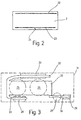
- Figure 2 shows the starting substrate 2 with a first Perforation strips 22 and a second perforation strip 23, another perforation strip 24 is assigned at right angles.
- the Perforation strips 22 and 23 are parallel and spaced apart along the long sides of the Output substrate 2 arranged.
- the starting substrate shown here is 2 shows a substrate in the “delivery state”. That is, the perforation strips 22, 23 and 24 are not open yet.
- FIG. 3 shows the mounting substrate 20 after it all necessary processing and assembly processes has passed through, here conductor tracks and components are not shown. Especially the mounting substrate 20 differs from the starting substrate 2 by opening the perforation strips 22, 23 and 24 and the spatial reorganization of the substrate strips 32, 33 and 34. The mounting substrate 20 is located accordingly in the "installed state”.
- Display instruments 25, 26 are exemplary here and 27 shown in dashed lines. There are also status indicators different vehicle functions shown, for example warning lights 28, 29 and a control lamp 30 for a direction indicator.
- the display instruments arranged here as examples 25, 26 and 27, warning lights 28, 29 and the control lamp 30 are part of a here only schematically shown instrument panel 31 of a motor vehicle, not shown here.
- Substrate strips 32, 33 and 34 released.
- the resulting substrate strips 32, 33 and 34 can be both in one plane relative to the main part of the mounting substrate 20 are shifted like this indicated by the substrate strips 32 and 33 will be folded down as well, as in the case of the Substrate strip 34 shown.
- Substrate strips 32, 33 and 34 can be saved in material firmly make an electrical connection between the display instruments 25, 26 and 27, the warning lights 28, 29 and the indicator light 30 manufacture.
- warning lights and indicator lights realized can be, including electronic Components and illuminants the respective display elements can be individually assigned.
- the perforated starting substrate enables a material-reduced and therefore inexpensive Manufacture of the display device and optimal use of the available substrate area.
- substrate strips which are formed after opening the perforation, both shifted in the plane and folded can be. Show folded substrate strips the advantage that with a one-sided assembly of the substrate in one operation or similar on the back of the substrate can be applied. This reduces the Processing costs.
Landscapes
- Engineering & Computer Science (AREA)
- Microelectronics & Electronic Packaging (AREA)
- Instrument Panels (AREA)
Applications Claiming Priority (2)
| Application Number | Priority Date | Filing Date | Title |
|---|---|---|---|
| DE19651863A DE19651863A1 (de) | 1996-12-13 | 1996-12-13 | Anzeigevorrichtung |
| DE19651863 | 1996-12-13 |
Publications (2)
| Publication Number | Publication Date |
|---|---|
| EP0848583A1 true EP0848583A1 (fr) | 1998-06-17 |
| EP0848583B1 EP0848583B1 (fr) | 2003-03-26 |
Family
ID=7814583
Family Applications (1)
| Application Number | Title | Priority Date | Filing Date |
|---|---|---|---|
| EP97117125A Expired - Lifetime EP0848583B1 (fr) | 1996-12-13 | 1997-10-02 | Dispositif d'affichage |
Country Status (2)
| Country | Link |
|---|---|
| EP (1) | EP0848583B1 (fr) |
| DE (2) | DE19651863A1 (fr) |
Cited By (1)
| Publication number | Priority date | Publication date | Assignee | Title |
|---|---|---|---|---|
| EP1168897A3 (fr) * | 2000-06-30 | 2004-01-02 | Coroplast Fritz Müller GmbH & Co. KG | Panneau à circuit imprimé en feuille mince et son procédé de fabrication et de montage |
Families Citing this family (1)
| Publication number | Priority date | Publication date | Assignee | Title |
|---|---|---|---|---|
| DE10029729A1 (de) * | 2000-06-16 | 2002-02-21 | Mannesmann Vdo Ag | Kombiinstrument zur Anzeige von Messwerten und/oder sonstigen Hinweisen, insbesondere zur Verwendung in einem Kraftfahrzeug |
Citations (4)
| Publication number | Priority date | Publication date | Assignee | Title |
|---|---|---|---|---|
| EP0126856A2 (fr) * | 1983-05-21 | 1984-12-05 | GRUNDIG E.M.V. Elektro-Mechanische Versuchsanstalt Max Grundig holländ. Stiftung & Co. KG. | Procédé de fabrication d'une plaquette de circuit comportant des domaines rigides et flexibles |
| US4569885A (en) * | 1981-08-20 | 1986-02-11 | Nitto Electric Industrial Company, Limited | Polyester film for forming printed circuit |
| DE3500899A1 (de) * | 1985-01-12 | 1986-07-17 | Benny S - car + boat Technik + Design Team GmbH, 5650 Solingen | Anzeigeinstrument mit quasi-kontinuierlicher darstellung |
| DE3904656A1 (de) * | 1989-02-16 | 1990-08-23 | Vdo Schindling | Zeigerinstrument |
-
1996
- 1996-12-13 DE DE19651863A patent/DE19651863A1/de not_active Withdrawn
-
1997
- 1997-10-02 DE DE59709619T patent/DE59709619D1/de not_active Expired - Lifetime
- 1997-10-02 EP EP97117125A patent/EP0848583B1/fr not_active Expired - Lifetime
Patent Citations (4)
| Publication number | Priority date | Publication date | Assignee | Title |
|---|---|---|---|---|
| US4569885A (en) * | 1981-08-20 | 1986-02-11 | Nitto Electric Industrial Company, Limited | Polyester film for forming printed circuit |
| EP0126856A2 (fr) * | 1983-05-21 | 1984-12-05 | GRUNDIG E.M.V. Elektro-Mechanische Versuchsanstalt Max Grundig holländ. Stiftung & Co. KG. | Procédé de fabrication d'une plaquette de circuit comportant des domaines rigides et flexibles |
| DE3500899A1 (de) * | 1985-01-12 | 1986-07-17 | Benny S - car + boat Technik + Design Team GmbH, 5650 Solingen | Anzeigeinstrument mit quasi-kontinuierlicher darstellung |
| DE3904656A1 (de) * | 1989-02-16 | 1990-08-23 | Vdo Schindling | Zeigerinstrument |
Cited By (1)
| Publication number | Priority date | Publication date | Assignee | Title |
|---|---|---|---|---|
| EP1168897A3 (fr) * | 2000-06-30 | 2004-01-02 | Coroplast Fritz Müller GmbH & Co. KG | Panneau à circuit imprimé en feuille mince et son procédé de fabrication et de montage |
Also Published As
| Publication number | Publication date |
|---|---|
| DE59709619D1 (de) | 2003-04-30 |
| DE19651863A1 (de) | 1998-06-18 |
| EP0848583B1 (fr) | 2003-03-26 |
Similar Documents
| Publication | Publication Date | Title |
|---|---|---|
| EP0382879B1 (fr) | Instrument muni d'une aiguille | |
| DE2913138A1 (de) | Anzeigevorrichtung | |
| DE3902956A1 (de) | Anordnung fuer eine instrumententafel oder einen instrumententafelteil, insbesondere fuer kraftfahrzeuge | |
| EP1019260A1 (fr) | Systeme de mesure, notamment pour dispositifs d'affichage en technique automobile | |
| DE2245415C3 (de) | Kompakter elektronischer Rechner | |
| DE19652139C1 (de) | Anzeigeeinheit | |
| DE19757545A1 (de) | Anzeigevorrichtung, insbesondere für ein Armaturenbrett | |
| EP0848583B1 (fr) | Dispositif d'affichage | |
| DE2611434A1 (de) | Beleuchtungseinrichtung fuer anzeigeinstrumente | |
| DE4440148A1 (de) | Rohrstückförmiges Gehäuse | |
| DE3113773C2 (fr) | ||
| EP0799406A1 (fr) | Indicateur | |
| EP0841542A1 (fr) | Dispositif d'affichage | |
| DE2546842A1 (de) | Instrumenten-anordnung | |
| DE2607398A1 (de) | Batteriebetriebene elektrische uhr | |
| EP0935740A1 (fr) | Instrument afficheur a plan d'affichage lumineux | |
| DE3735004A1 (de) | Anzeigevorrichtung | |
| DE29618395U1 (de) | Anzeigeinstrument mit einem beleuchtbaren Anzeigefeld | |
| EP0755822A2 (fr) | Dispositif d'affichage pour des fonctions et des états de fonctionnement d'une automobile | |
| EP1136870B1 (fr) | Dispositif d'affichage | |
| DE10202955A1 (de) | Modulare Innenleuchte für ein Kraftfahrzeug | |
| AT408283B (de) | Türsprechanlage mit einer geräte-frontplatte | |
| DE2903830A1 (de) | Elektrischer verbinder fuer kraftfahrzeuge | |
| DE1817530C3 (de) | Halterungsanordnung für ein Anzeigeinstrument | |
| EP2567853A2 (fr) | Élément de fixation pour un moteur électrique sur une plaquette électronique, dispositif d'affichage d'un véhicule automobile comprenant un instrument à aiguille électrique avec moteur électrique fixé sur une plaquette électronique au moyen d'un tel élément de fixation ainsi que le procédé de fixation d'un moteur électrique sur une plaquette électronique avec un tel élément de fixation |
Legal Events
| Date | Code | Title | Description |
|---|---|---|---|
| PUAI | Public reference made under article 153(3) epc to a published international application that has entered the european phase |
Free format text: ORIGINAL CODE: 0009012 |
|
| AK | Designated contracting states |
Kind code of ref document: A1 Designated state(s): DE FR GB IT |
|
| AX | Request for extension of the european patent |
Free format text: AL;LT;LV;RO;SI |
|
| 17P | Request for examination filed |
Effective date: 19981217 |
|
| AKX | Designation fees paid |
Free format text: DE FR GB IT |
|
| RBV | Designated contracting states (corrected) |
Designated state(s): DE FR GB IT |
|
| 17Q | First examination report despatched |
Effective date: 19990315 |
|
| GRAH | Despatch of communication of intention to grant a patent |
Free format text: ORIGINAL CODE: EPIDOS IGRA |
|
| GRAH | Despatch of communication of intention to grant a patent |
Free format text: ORIGINAL CODE: EPIDOS IGRA |
|
| GRAA | (expected) grant |
Free format text: ORIGINAL CODE: 0009210 |
|
| AK | Designated contracting states |
Designated state(s): DE FR GB IT |
|
| REG | Reference to a national code |
Ref country code: GB Ref legal event code: FG4D Free format text: NOT ENGLISH |
|
| REF | Corresponds to: |
Ref document number: 59709619 Country of ref document: DE Date of ref document: 20030430 Kind code of ref document: P |
|
| GBT | Gb: translation of ep patent filed (gb section 77(6)(a)/1977) | ||
| ET | Fr: translation filed | ||
| PLBE | No opposition filed within time limit |
Free format text: ORIGINAL CODE: 0009261 |
|
| STAA | Information on the status of an ep patent application or granted ep patent |
Free format text: STATUS: NO OPPOSITION FILED WITHIN TIME LIMIT |
|
| 26N | No opposition filed |
Effective date: 20031230 |
|
| PGFP | Annual fee paid to national office [announced via postgrant information from national office to epo] |
Ref country code: IT Payment date: 20091023 Year of fee payment: 13 Ref country code: GB Payment date: 20091023 Year of fee payment: 13 Ref country code: FR Payment date: 20091110 Year of fee payment: 13 |
|
| PGFP | Annual fee paid to national office [announced via postgrant information from national office to epo] |
Ref country code: DE Payment date: 20091215 Year of fee payment: 13 |
|
| GBPC | Gb: european patent ceased through non-payment of renewal fee |
Effective date: 20101002 |
|
| PG25 | Lapsed in a contracting state [announced via postgrant information from national office to epo] |
Ref country code: FR Free format text: LAPSE BECAUSE OF NON-PAYMENT OF DUE FEES Effective date: 20101102 |
|
| REG | Reference to a national code |
Ref country code: FR Ref legal event code: ST Effective date: 20110630 |
|
| REG | Reference to a national code |
Ref country code: DE Ref legal event code: R119 Ref document number: 59709619 Country of ref document: DE Effective date: 20110502 |
|
| PG25 | Lapsed in a contracting state [announced via postgrant information from national office to epo] |
Ref country code: GB Free format text: LAPSE BECAUSE OF NON-PAYMENT OF DUE FEES Effective date: 20101002 |
|
| PG25 | Lapsed in a contracting state [announced via postgrant information from national office to epo] |
Ref country code: IT Free format text: LAPSE BECAUSE OF NON-PAYMENT OF DUE FEES Effective date: 20101002 |
|
| PG25 | Lapsed in a contracting state [announced via postgrant information from national office to epo] |
Ref country code: DE Free format text: LAPSE BECAUSE OF NON-PAYMENT OF DUE FEES Effective date: 20110502 |