EP0849854A2 - Bloc électronique d'alimentation à découpage - Google Patents
Bloc électronique d'alimentation à découpage Download PDFInfo
- Publication number
- EP0849854A2 EP0849854A2 EP97121481A EP97121481A EP0849854A2 EP 0849854 A2 EP0849854 A2 EP 0849854A2 EP 97121481 A EP97121481 A EP 97121481A EP 97121481 A EP97121481 A EP 97121481A EP 0849854 A2 EP0849854 A2 EP 0849854A2
- Authority
- EP
- European Patent Office
- Prior art keywords
- transistor
- switching
- switching element
- power supply
- electronic
- Prior art date
- Legal status (The legal status is an assumption and is not a legal conclusion. Google has not performed a legal analysis and makes no representation as to the accuracy of the status listed.)
- Granted
Links
Images

Classifications
-
- H—ELECTRICITY
- H03—ELECTRONIC CIRCUITRY
- H03K—PULSE TECHNIQUE
- H03K17/00—Electronic switching or gating, i.e. not by contact-making and –breaking
- H03K17/51—Electronic switching or gating, i.e. not by contact-making and –breaking characterised by the components used
- H03K17/78—Electronic switching or gating, i.e. not by contact-making and –breaking characterised by the components used using opto-electronic devices, i.e. light-emitting and photoelectric devices electrically- or optically-coupled
- H03K17/785—Electronic switching or gating, i.e. not by contact-making and –breaking characterised by the components used using opto-electronic devices, i.e. light-emitting and photoelectric devices electrically- or optically-coupled controlling field-effect transistor switches
-
- H—ELECTRICITY
- H02—GENERATION; CONVERSION OR DISTRIBUTION OF ELECTRIC POWER
- H02H—EMERGENCY PROTECTIVE CIRCUIT ARRANGEMENTS
- H02H9/00—Emergency protective circuit arrangements for limiting excess current or voltage without disconnection
- H02H9/001—Emergency protective circuit arrangements for limiting excess current or voltage without disconnection limiting speed of change of electric quantities, e.g. soft switching on or off
-
- H—ELECTRICITY
- H02—GENERATION; CONVERSION OR DISTRIBUTION OF ELECTRIC POWER
- H02M—APPARATUS FOR CONVERSION BETWEEN AC AND AC, BETWEEN AC AND DC, OR BETWEEN DC AND DC, AND FOR USE WITH MAINS OR SIMILAR POWER SUPPLY SYSTEMS; CONVERSION OF DC OR AC INPUT POWER INTO SURGE OUTPUT POWER; CONTROL OR REGULATION THEREOF
- H02M1/00—Details of apparatus for conversion
- H02M1/32—Means for protecting converters other than automatic disconnection
-
- H—ELECTRICITY
- H02—GENERATION; CONVERSION OR DISTRIBUTION OF ELECTRIC POWER
- H02M—APPARATUS FOR CONVERSION BETWEEN AC AND AC, BETWEEN AC AND DC, OR BETWEEN DC AND DC, AND FOR USE WITH MAINS OR SIMILAR POWER SUPPLY SYSTEMS; CONVERSION OF DC OR AC INPUT POWER INTO SURGE OUTPUT POWER; CONTROL OR REGULATION THEREOF
- H02M1/00—Details of apparatus for conversion
- H02M1/36—Means for starting or stopping converters
-
- H—ELECTRICITY
- H02—GENERATION; CONVERSION OR DISTRIBUTION OF ELECTRIC POWER
- H02M—APPARATUS FOR CONVERSION BETWEEN AC AND AC, BETWEEN AC AND DC, OR BETWEEN DC AND DC, AND FOR USE WITH MAINS OR SIMILAR POWER SUPPLY SYSTEMS; CONVERSION OF DC OR AC INPUT POWER INTO SURGE OUTPUT POWER; CONTROL OR REGULATION THEREOF
- H02M3/00—Conversion of DC power input into DC power output
- H02M3/02—Conversion of DC power input into DC power output without intermediate conversion into AC
- H02M3/04—Conversion of DC power input into DC power output without intermediate conversion into AC by static converters
- H02M3/10—Conversion of DC power input into DC power output without intermediate conversion into AC by static converters using discharge tubes with control electrode or semiconductor devices with control electrode
- H02M3/145—Conversion of DC power input into DC power output without intermediate conversion into AC by static converters using discharge tubes with control electrode or semiconductor devices with control electrode using devices of a triode or transistor type requiring continuous application of a control signal
- H02M3/155—Conversion of DC power input into DC power output without intermediate conversion into AC by static converters using discharge tubes with control electrode or semiconductor devices with control electrode using devices of a triode or transistor type requiring continuous application of a control signal using semiconductor devices only
- H02M3/156—Conversion of DC power input into DC power output without intermediate conversion into AC by static converters using discharge tubes with control electrode or semiconductor devices with control electrode using devices of a triode or transistor type requiring continuous application of a control signal using semiconductor devices only with automatic control of output voltage or current, e.g. switching regulators
- H02M3/158—Conversion of DC power input into DC power output without intermediate conversion into AC by static converters using discharge tubes with control electrode or semiconductor devices with control electrode using devices of a triode or transistor type requiring continuous application of a control signal using semiconductor devices only with automatic control of output voltage or current, e.g. switching regulators including plural semiconductor devices as final control devices for a single load
Definitions
- the invention relates to an electronic switching power supply according to the preamble of claim 1.
- Switched-mode power supplies for direct current supply to a load, which are fed from an AC mains voltage, are known in a number of embodiments. Tietze-Schenk, for example, provides an overview of the circuit principles used for this Semiconductor Circuit Technology ", Springer Verlag Berlin, 9th edition 1989 in section 18.5 Switched-mode power supplies ", p. 561 ff. Put simply, such switched-mode power supplies comprise a rectifier circuit connected to the supplying AC voltage, which is often designed as a rectifier bridge.
- the rectifier circuit supplies a pulsating DC voltage, which is converted into a smoothed DC voltage in an output stage of the switched-mode power supply connected to it.
- these output stages can be designed differently depending on the application, for example as a forward or flyback converter.
- DE-A-34 02 222 is a circuit arrangement for limiting overvoltages in DC electrical systems known.
- the comparator compares it to it signals fed to both of its inputs and controls the Switches such that a connected to this circuit arrangement Device is disconnected from the mains in the event of overvoltages.
- the controllable switch can also be used as a semiconductor switch be trained. This is made possible by means of one in its control circuit lying capacitor at a high capacitive Load from the connected device the high inrush current to reduce.
- EP-A-0 423 885 is a power supply device known with a circuit for inrush current limitation.
- This circuit has a first semiconductor switch on whose switching path together with one of them in parallel resistance in the low potential Supply line is switched on.
- the switching path of a second semiconductor switch intended.
- the control electrode of the second semiconductor switch is connected to the tap of a voltage divider, which in turn has a second capacitor in parallel lies.
- the switching path of a third semiconductor switch between the tap of the voltage divider and connected to the supply line at low potential. This third semiconductor switch becomes dependent one supplied by a threshold circuit Control current controlled so that it falls below a predetermined threshold value of the supply voltage blocks.
- the last-mentioned known circuit arrangement is - with all functional advantages - very complex in terms of circuit technology.
- Both known circuit arrangements also have in common that they separate a connected output stage or a device supplied with the supply voltage from the direct current supply by a switch coupled into the supply or mains line which is at a low potential, they are switching power supplies with so-called Low-side "switches.
- This supply line is usually at ground reference potential. This can result in a different ground reference potential in the different operating states on different modules, which must be taken into account when designing the circuit and can make implementation of the circuit very difficult.
- the present invention is therefore based on the object to further develop a switching power supply of the type mentioned at the beginning, that a controlled with little effort Switching the rectified AC line voltage in the high potential branch of its supply with a inexpensive power semiconductor switch performed so an interruption of the low potential Supply line avoided and at the same time a controlled Current limitation is made possible.
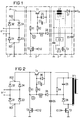
- FIG. 1 is a switching power supply with an output stage as an example selected as the step-up converter of an electronic Ballast designed for fluorescent lamps is.
- an AC line voltage u ⁇ - if necessary via a harmonic filter, not shown -
- a rectifier bridge 1 which consists of four diodes D1 to D4 is constructed and has two outputs RO1 and RO2. The one output is RO1 of the rectifier bridge 1 connected to ground reference potential.
- At the second exit RO2, which is at high potential is given by rectifier bridge 1 a rectified derived from the AC line voltage u ⁇ Voltage U + off.
- This second output RO2 of the rectifier bridge 1 is over an electronic switch 2, which will be described in more detail below is explained with the input of a step-up converter 3 connected.
- a choke L1 is connected, which on the other hand via a charging diode polarized in the forward direction D7 with the positive pole of an electrolytic capacitor Storage capacitor C5 is connected, the second Pole is connected to ground reference potential.
- the connection point between inductor L1 and charging diode D7 is over the switching distance of a switching transistor T3 also at ground reference potential placed.
- the positive pole of the storage capacitor C5 forms the output of the step-up converter 3, at which a step-up, smoothed DC voltage Ua to a in FIG Lamp circuit is no longer shown.
- the circuit arrangement described above is for electronic Ballasts for fluorescent lamps as such to look familiar.
- the rectifier bridge 1 With the help of the rectifier bridge 1 the rectified, pulsating DC voltage U + generated and via the electronic Switch 2 fed to the step-up converter 3. Is the switching transistor T3 switched on, the current in the Throttle L1 is essentially linear.
- the Switching transistor T3 opened again and the described Function repeats itself. It serves as the setpoint for the Deactivation times of the switching transistor T3 the instantaneous value the rectified pulsating voltage U +.
- the Storage capacitor C5 In the sequence of these processes, which are compared to the Mains frequency with a higher repetition frequency, the Storage capacitor C5 to the smoothed output voltage Ua of the switching power supply, whose level is above the peak value the rectified voltage U +.
- control signals Ct3 are to be fed to it. How these control signals Ct3 can be generated is quite familiar to the expert and here of minor importance Meaning. Therefore, in Figure 1 is only exemplary in broken lines and schematic in a block diagram indicated such a possibility.
- a signal generator CG detects the instantaneous value of the rectified voltage U +, further via an auxiliary winding L11 of the choke L1 Unloading processes and the current state of charge of the storage capacitor C5 and generated from these detection signals the control signals for the switching transistor T3.
- the step-up converter 3 which in conjunction with the rectifier bridge 1 conventionally forms the power supply of an electronic ballast for fluorescent lamps, a relatively high inrush current results when the storage capacitor C5, which is initially discharged during commissioning, is charged.
- the electronic switch 2 is now arranged between the rectifier bridge 1 and the step-up converter 3.
- This transistor switching element T1 which is designed in particular as an N-channel semiconductor switching element and is arranged with its switching path between the high potential output RO2 of the rectifier bridge 1 and the corresponding input of the step-up converter 3.
- This transistor switching element can, depending on the application, as a MOSFET may be formed as an IGBT (Insulated Gate Bipolar Transistor T) or as another bipolar power transistor.
- Another switching transistor T2 is arranged with its switching path via a series resistor R1, located in front of the transistor switching element T1, between the input of the electronic switch 2, which is at high potential, and the ground reference potential.
- the connection point A of the series resistor R1 with the second switching transistor T2 is connected to the control input of the transistor switching element T1 via an input resistor R2.
- this connection point A is connected via the series circuit of a further resistor R3 and a coupling diode D6 to the high potential of the storage capacitor C5.
- a parallel connection of a Zener diode D5 and a further capacitor C3 is provided between the emitter output of the transistor switching element T1 and its control input.
- the electronic switch 2 remains deactivated and disconnects the output of the rectifier bridge 1 from that to high Potential input of the step-up converter 3, if the second switching transistor T2 via a corresponding him supplied control signal Ct2 is turned on. Because then the connection point A lies between this second one Switching transistor and the series resistor R1 to ground reference potential and blocks the transistor switching element T1.
- the second switching transistor T2 In order to switch the electronic switch 2 on, the second switching transistor T2 is blocked. In this condition of the second switching transistor T2 current flows through the Series resistor R1 and the input resistor R2, with which the coupled to the control input of the transistor switching element T1 Capacitor C3 is charged.
- the tension increases conditional at the control input of the transistor switching element T1 by the time constant of the RC element with the resistors R1, R2 and capacitor C3, slowly on.
- the transistor switching element T1 is also not immediately switched on, but switched on in a continuous transition. That is, it becomes the active area of the transistor switching element Drive through T1 slowly and the inrush current of the connected boost converter 3 to a predetermined one Limited peak.
- the storage capacitor C5 charges of the step-up converter 3 accordingly slowly to the peak value the mains AC voltage u ⁇ . Then the switching transistor T3 controlled. In the stationary state of the step-up converter 3 finally stands the boosted output voltage Among others available. Only then is the control input an auxiliary voltage is supplied to the transistor switching element T1, which is greater than the instantaneous value of the electronic switch 2 supplied rectified voltage U +.
- This Auxiliary voltage becomes the output side of the switching power supply itself taken and in the example of the circuit arrangement of Figure 1 on the control input of the transistor switching element T1 the coupling diode D6 and the resistors R3, R2 supplied.
- the transistor switching element T1 finally controlled into saturation, so that then its current-limiting effect is eliminated.
- the explained limitation of the inrush current of the step-up converter 3 or more generally that of the electronic switch connected output stage of the power supply means not only that of the components located in the current path in question be less burdened when switching on, what contributes to their extension of the lifespan and if necessary also allows a more favorable dimensioning.
- the transistor switching element T1 in the high potential current path is arranged and only affects this, any influence on that Ground reference potential of the switching power supply avoided and thus the disadvantages mentioned at the outset are excluded.
- circuitry becomes simple Way a switch in the high potential Current path realized with the commercially available N-channel semiconductor switching elements is to be implemented. This is more advantageous than P-channel types with their known ones To have disadvantages.
- FIG 2 is another embodiment for a the switching power supply operating principle explained above shown, the output stage in this case as Flyback converter 31 is formed.
- Flyback converters are as such well known, so that it is sufficient to point out that in this case the throttle L1 of the embodiment extended from Figure 1 to a transformer TF1 is, whose primary winding - analogous to the embodiment of Figure 1 - via the switching transistor T3 at ground reference potential is laid. All others, otherwise with the one in figure 1 illustrated embodiment at least functionally matching components of the circuit arrangement designated with the same reference numerals. Especially this also applies to the storage capacitor CS in this Case of the primary winding of the transformer TF1 lying in parallel is arranged.
- the embodiment shown in Figure 3 differs differs only from the exemplary embodiment according to FIG with respect to that connected in parallel with the primary winding of the transformer TF1 Voltage limiting network. In this case is that from the resistor R4 and the capacitor C6 after Figure 2 formed RC element replaced by another Z-diode D9.
- FIG. 4 shows an alternative in a further exemplary embodiment for driving the transistor switching element T1 shown.
- this alternative can be used in general it is here, for the sake of simplicity, in connection with the step-up converter selected for the first exemplary embodiment 3 shown, so that at this point only on the Circuit differences to Figure 1 is to be pointed out.
- the control of the Transistor switching element T1 galvanically decoupled by instead of the second switching transistor T2 an optocoupler OC1 is arranged in the network that is the control input of the Transistor switching element T 1 is assigned.
- this optocoupler OC1 at its control inputs Control signals Ct01 or Ct02 are supplied the control signals Ct2 of the second switching transistor T2 in 1 correspond functionally to the embodiment of FIG.
- the output side of the optocoupler OC1 is in the control network of the transistor switching element T1 between the capacitor C3 and the resistor R3 arranged over the - as in the embodiment 1 - the transistor switching element T1 again the auxiliary voltage required for saturation operation is fed.
- the Voltage at the control input of the transistor switching element T1 below the threshold voltage and thus this locked, so as long as the output transistor of the optocoupler OC1 conducts. If, on the other hand, the optocoupler OC1 is blocked, then in this case via the series resistor R1 between the emitter and control input of the transistor switching element T1 lying Capacitor C3 charged and thus the switch-on function of the Transistor switching element T1 initiated, already in detail described with reference to the embodiment of Figure 1 was and therefore need not be explained again.
Landscapes
- Engineering & Computer Science (AREA)
- Power Engineering (AREA)
- Dc-Dc Converters (AREA)
- Rectifiers (AREA)
- Stand-By Power Supply Arrangements (AREA)
- Circuits Of Receivers In General (AREA)
Applications Claiming Priority (2)
| Application Number | Priority Date | Filing Date | Title |
|---|---|---|---|
| DE19652808 | 1996-12-18 | ||
| DE19652808 | 1996-12-18 |
Publications (3)
| Publication Number | Publication Date |
|---|---|
| EP0849854A2 true EP0849854A2 (fr) | 1998-06-24 |
| EP0849854A3 EP0849854A3 (fr) | 1999-07-14 |
| EP0849854B1 EP0849854B1 (fr) | 2003-06-18 |
Family
ID=7815227
Family Applications (1)
| Application Number | Title | Priority Date | Filing Date |
|---|---|---|---|
| EP97121481A Expired - Lifetime EP0849854B1 (fr) | 1996-12-18 | 1997-12-05 | Bloc électronique d'alimentation à découpage |
Country Status (4)
| Country | Link |
|---|---|
| US (1) | US5877614A (fr) |
| EP (1) | EP0849854B1 (fr) |
| AT (1) | ATE243384T1 (fr) |
| DE (1) | DE59710304D1 (fr) |
Cited By (2)
| Publication number | Priority date | Publication date | Assignee | Title |
|---|---|---|---|---|
| US7432690B2 (en) | 2005-05-27 | 2008-10-07 | Hubbell Incorporated | Dual circuit wall switch occupancy sensor and method of operating same |
| WO2021197997A1 (fr) * | 2020-03-30 | 2021-10-07 | Freifrau von Fürstenberg, Stephanie | Circuit pour limiter le courant d'appel |
Families Citing this family (6)
| Publication number | Priority date | Publication date | Assignee | Title |
|---|---|---|---|---|
| JP2000197365A (ja) * | 1998-12-24 | 2000-07-14 | Denso Corp | 直流電源回路 |
| US6377164B1 (en) | 1999-03-10 | 2002-04-23 | Chester C. Fulmer | High powered tri-mode light show |
| KR100491599B1 (ko) * | 2002-08-29 | 2005-05-27 | 삼성전자주식회사 | 고압전원장치 |
| DE102005030123B4 (de) * | 2005-06-28 | 2017-08-31 | Austriamicrosystems Ag | Stromversorgungsanordnung und deren Verwendung |
| CN101606435B (zh) * | 2007-02-13 | 2011-04-13 | 奥斯兰姆有限公司 | 用于驱动至少一个发光二极管的发光二极管模块和方法 |
| US11476772B2 (en) * | 2019-07-31 | 2022-10-18 | Epistar Corporation | Voltage converter circuit for converting AC voltage to DC voltage |
Family Cites Families (13)
| Publication number | Priority date | Publication date | Assignee | Title |
|---|---|---|---|---|
| DE3402222A1 (de) * | 1984-01-24 | 1985-07-25 | Licentia Patent-Verwaltungs-Gmbh, 6000 Frankfurt | Schaltungsanordnung zum begrenzen von ueberspannungen |
| DE3722337A1 (de) * | 1987-07-07 | 1989-01-19 | Philips Patentverwaltung | Schaltungsanordnung zum uebertragen elektrischer energie |
| DE3840305A1 (de) * | 1988-11-30 | 1990-05-31 | Philips Patentverwaltung | Schaltungsanordnung zum speisen einer last |
| GB2226195A (en) * | 1988-12-15 | 1990-06-20 | Philips Nv | A transient protection circuit |
| FI85633C (fi) * | 1989-05-08 | 1992-05-11 | Telenokia Oy | Spaenningsfoerhoejningsregulator. |
| US5068572A (en) * | 1989-06-08 | 1991-11-26 | U.S. Philips Corporation | Switch mode power supply |
| DE3934577A1 (de) * | 1989-10-17 | 1991-04-18 | Philips Patentverwaltung | Stromversorgungseinrichtung mit einschaltstrombegrenzungsschaltung |
| US5198743A (en) * | 1990-12-11 | 1993-03-30 | Span, Inc. | Battery charger with microprocessor control |
| EP0590304B1 (fr) * | 1992-09-30 | 1998-07-08 | Siemens Aktiengesellschaft | Procédé pour la commande pilote d'une alimentation en courant commutée pour légalisation de la tension d'alimentation |
| US5283707A (en) * | 1992-11-27 | 1994-02-01 | Northern Telecom Limited | Inrush current limiting circuit |
| JP2784136B2 (ja) * | 1993-10-19 | 1998-08-06 | 浜松ホトニクス株式会社 | スイッチング電源の過負荷・短絡保護回路 |
| DE4421806C1 (de) * | 1994-06-22 | 1995-08-10 | Siemens Ag | Schaltnetzteil mit sinusförmiger Stromaufnahme |
| US5694025A (en) * | 1996-04-23 | 1997-12-02 | Motorola, Inc. | Battery charger with control circuit |
-
1997
- 1997-12-05 DE DE59710304T patent/DE59710304D1/de not_active Expired - Lifetime
- 1997-12-05 EP EP97121481A patent/EP0849854B1/fr not_active Expired - Lifetime
- 1997-12-05 AT AT97121481T patent/ATE243384T1/de not_active IP Right Cessation
- 1997-12-16 US US08/991,934 patent/US5877614A/en not_active Expired - Lifetime
Cited By (3)
| Publication number | Priority date | Publication date | Assignee | Title |
|---|---|---|---|---|
| US7432690B2 (en) | 2005-05-27 | 2008-10-07 | Hubbell Incorporated | Dual circuit wall switch occupancy sensor and method of operating same |
| US7830133B2 (en) | 2005-05-27 | 2010-11-09 | Hubbell Incorporated | Dual circuit wall switch occupancy sensor and method of operating same |
| WO2021197997A1 (fr) * | 2020-03-30 | 2021-10-07 | Freifrau von Fürstenberg, Stephanie | Circuit pour limiter le courant d'appel |
Also Published As
| Publication number | Publication date |
|---|---|
| EP0849854A3 (fr) | 1999-07-14 |
| ATE243384T1 (de) | 2003-07-15 |
| EP0849854B1 (fr) | 2003-06-18 |
| US5877614A (en) | 1999-03-02 |
| DE59710304D1 (de) | 2003-07-24 |
Similar Documents
| Publication | Publication Date | Title |
|---|---|---|
| DE69729294T2 (de) | Niedrigpreis-, Hochspannungs-, Flyback-Stromversorgung | |
| DE102011087368B4 (de) | Treiberschaltung, Anordnung und Verfahren zum Bootstrapping eines Schaltertreibers | |
| EP1920525B1 (fr) | Dispositif de commande conçu pour un convertisseur de tension, et procede | |
| DE2834512C2 (de) | Umformer mit ausschaltbaren Thyristoren | |
| EP2026457A1 (fr) | Onduleur avec deux circuits intermédiaires | |
| EP2089961A1 (fr) | Convertisseur cc/cc autohétérodyne et procédé à cet effet | |
| DE102014107815A1 (de) | System und Verfahren zum Ansteuern von Transistoren | |
| DE102012216691A1 (de) | Stromrichterschaltung und Verfahren zur Steuerung der Stromrichterschaltung | |
| EP2026456A1 (fr) | Onduleur | |
| DE102004016927A1 (de) | Verfahren zur Strom- und Spannungsregelung für ein Schaltnetzteil | |
| DE4421249C2 (de) | Schaltstromversorgungsgerät mit Snubber-Schaltung | |
| EP0849854B1 (fr) | Bloc électronique d'alimentation à découpage | |
| EP0201878A2 (fr) | Circuit à transistor MOS à canal N commutant un potentiel positif | |
| DE102005016047A1 (de) | Umschaltbarer Spannungswandler | |
| EP2168229A1 (fr) | Ensemble circuit pourvu d'un transformateur de tension et procédé correspondant | |
| EP2208400A1 (fr) | Alimentation en courant commutable pour circuits auxiliaires dans un convertisseur | |
| WO1993012630A1 (fr) | Dispositif utilise pour faire fonctionner une lampe a decharge | |
| DE19614816C1 (de) | Elektronisches Schaltnetzteil und dessen Verwendung | |
| DE10257908A1 (de) | Getaktete Leistungsversorgung | |
| EP0009225B1 (fr) | Circuit de protection | |
| DE102019104652B4 (de) | Leistungselektronische Vorrichtung und Verfahren zur elektrischen Spannungsversorgung einer Treiberschaltung eines Leistungshalbleiterschalters | |
| DE3300285C2 (de) | Elektronisches Schaltnetzteil | |
| EP0854562B1 (fr) | Alimentation de puissance à decoupape | |
| DE3311737C2 (de) | Elektronisches Schaltnetzteil | |
| DE102007052669B4 (de) | Vorschaltgerät für eine Gasentladungslampe, bspw. eine HID-Lampe |
Legal Events
| Date | Code | Title | Description |
|---|---|---|---|
| PUAI | Public reference made under article 153(3) epc to a published international application that has entered the european phase |
Free format text: ORIGINAL CODE: 0009012 |
|
| AK | Designated contracting states |
Kind code of ref document: A2 Designated state(s): AT CH DE FR GB IT LI NL SE |
|
| AX | Request for extension of the european patent |
Free format text: AL;LT;LV;MK;RO;SI |
|
| PUAL | Search report despatched |
Free format text: ORIGINAL CODE: 0009013 |
|
| AK | Designated contracting states |
Kind code of ref document: A3 Designated state(s): AT BE CH DE DK ES FI FR GB GR IE IT LI LU MC NL PT SE |
|
| AX | Request for extension of the european patent |
Free format text: AL;LT;LV;MK;RO;SI |
|
| RIC1 | Information provided on ipc code assigned before grant |
Free format text: 6H 02H 9/02 A, 6H 02M 3/335 B |
|
| 17P | Request for examination filed |
Effective date: 19991217 |
|
| AKX | Designation fees paid |
Free format text: AT CH DE FR GB IT LI NL SE |
|
| RAP1 | Party data changed (applicant data changed or rights of an application transferred) |
Owner name: PATENT-TREUHAND-GESELLSCHAFT FUER ELEKTRISCHE GLUE |
|
| 17Q | First examination report despatched |
Effective date: 20010430 |
|
| GRAH | Despatch of communication of intention to grant a patent |
Free format text: ORIGINAL CODE: EPIDOS IGRA |
|
| GRAH | Despatch of communication of intention to grant a patent |
Free format text: ORIGINAL CODE: EPIDOS IGRA |
|
| GRAA | (expected) grant |
Free format text: ORIGINAL CODE: 0009210 |
|
| AK | Designated contracting states |
Designated state(s): AT CH DE FR GB IT LI NL SE |
|
| REG | Reference to a national code |
Ref country code: GB Ref legal event code: FG4D Free format text: NOT ENGLISH |
|
| REG | Reference to a national code |
Ref country code: CH Ref legal event code: NV Representative=s name: SERVOPATENT GMBH Ref country code: CH Ref legal event code: EP |
|
| REF | Corresponds to: |
Ref document number: 59710304 Country of ref document: DE Date of ref document: 20030724 Kind code of ref document: P |
|
| REG | Reference to a national code |
Ref country code: SE Ref legal event code: TRGR |
|
| GBT | Gb: translation of ep patent filed (gb section 77(6)(a)/1977) |
Effective date: 20031006 |
|
| PLBE | No opposition filed within time limit |
Free format text: ORIGINAL CODE: 0009261 |
|
| STAA | Information on the status of an ep patent application or granted ep patent |
Free format text: STATUS: NO OPPOSITION FILED WITHIN TIME LIMIT |
|
| ET | Fr: translation filed | ||
| 26N | No opposition filed |
Effective date: 20040319 |
|
| PGFP | Annual fee paid to national office [announced via postgrant information from national office to epo] |
Ref country code: AT Payment date: 20051123 Year of fee payment: 9 |
|
| PGFP | Annual fee paid to national office [announced via postgrant information from national office to epo] |
Ref country code: NL Payment date: 20051205 Year of fee payment: 9 |
|
| PGFP | Annual fee paid to national office [announced via postgrant information from national office to epo] |
Ref country code: SE Payment date: 20051208 Year of fee payment: 9 Ref country code: GB Payment date: 20051208 Year of fee payment: 9 |
|
| PGFP | Annual fee paid to national office [announced via postgrant information from national office to epo] |
Ref country code: FR Payment date: 20051216 Year of fee payment: 9 |
|
| PGFP | Annual fee paid to national office [announced via postgrant information from national office to epo] |
Ref country code: CH Payment date: 20060308 Year of fee payment: 9 |
|
| PG25 | Lapsed in a contracting state [announced via postgrant information from national office to epo] |
Ref country code: SE Free format text: LAPSE BECAUSE OF NON-PAYMENT OF DUE FEES Effective date: 20061206 |
|
| PG25 | Lapsed in a contracting state [announced via postgrant information from national office to epo] |
Ref country code: LI Free format text: LAPSE BECAUSE OF NON-PAYMENT OF DUE FEES Effective date: 20061231 Ref country code: CH Free format text: LAPSE BECAUSE OF NON-PAYMENT OF DUE FEES Effective date: 20061231 |
|
| PGFP | Annual fee paid to national office [announced via postgrant information from national office to epo] |
Ref country code: IT Payment date: 20061231 Year of fee payment: 10 |
|
| PG25 | Lapsed in a contracting state [announced via postgrant information from national office to epo] |
Ref country code: NL Free format text: LAPSE BECAUSE OF NON-PAYMENT OF DUE FEES Effective date: 20070701 |
|
| REG | Reference to a national code |
Ref country code: CH Ref legal event code: PL |
|
| EUG | Se: european patent has lapsed | ||
| GBPC | Gb: european patent ceased through non-payment of renewal fee |
Effective date: 20061205 |
|
| NLV4 | Nl: lapsed or anulled due to non-payment of the annual fee |
Effective date: 20070701 |
|
| REG | Reference to a national code |
Ref country code: FR Ref legal event code: ST Effective date: 20070831 |
|
| PG25 | Lapsed in a contracting state [announced via postgrant information from national office to epo] |
Ref country code: GB Free format text: LAPSE BECAUSE OF NON-PAYMENT OF DUE FEES Effective date: 20061205 Ref country code: AT Free format text: LAPSE BECAUSE OF NON-PAYMENT OF DUE FEES Effective date: 20061205 |
|
| PG25 | Lapsed in a contracting state [announced via postgrant information from national office to epo] |
Ref country code: FR Free format text: LAPSE BECAUSE OF NON-PAYMENT OF DUE FEES Effective date: 20070102 |
|
| PG25 | Lapsed in a contracting state [announced via postgrant information from national office to epo] |
Ref country code: IT Free format text: LAPSE BECAUSE OF NON-PAYMENT OF DUE FEES Effective date: 20071205 |
|
| PGFP | Annual fee paid to national office [announced via postgrant information from national office to epo] |
Ref country code: DE Payment date: 20110221 Year of fee payment: 14 |
|
| REG | Reference to a national code |
Ref country code: DE Ref legal event code: R119 Ref document number: 59710304 Country of ref document: DE Effective date: 20120703 |
|
| PG25 | Lapsed in a contracting state [announced via postgrant information from national office to epo] |
Ref country code: DE Free format text: LAPSE BECAUSE OF NON-PAYMENT OF DUE FEES Effective date: 20120703 |