EP0851429A2 - Dispositif de détection de données et méthode pour cellule de mémoire multibit - Google Patents
Dispositif de détection de données et méthode pour cellule de mémoire multibit Download PDFInfo
- Publication number
- EP0851429A2 EP0851429A2 EP97109419A EP97109419A EP0851429A2 EP 0851429 A2 EP0851429 A2 EP 0851429A2 EP 97109419 A EP97109419 A EP 97109419A EP 97109419 A EP97109419 A EP 97109419A EP 0851429 A2 EP0851429 A2 EP 0851429A2
- Authority
- EP
- European Patent Office
- Prior art keywords
- data
- memory cell
- signal
- clock signal
- reference voltage
- Prior art date
- Legal status (The legal status is an assumption and is not a legal conclusion. Google has not performed a legal analysis and makes no representation as to the accuracy of the status listed.)
- Granted
Links
- 230000015654 memory Effects 0.000 title claims abstract description 104
- 238000000034 method Methods 0.000 title claims abstract description 22
- 230000004044 response Effects 0.000 claims abstract description 10
- 238000004519 manufacturing process Methods 0.000 claims description 5
- 230000000903 blocking effect Effects 0.000 claims description 2
- 238000010586 diagram Methods 0.000 description 4
- 239000003990 capacitor Substances 0.000 description 3
- 230000000630 rising effect Effects 0.000 description 3
- 238000012986 modification Methods 0.000 description 2
- 230000004048 modification Effects 0.000 description 2
- 239000004065 semiconductor Substances 0.000 description 2
- 238000003860 storage Methods 0.000 description 2
- 241000131943 Ascaridia compar Species 0.000 description 1
- 238000013500 data storage Methods 0.000 description 1
- 238000009826 distribution Methods 0.000 description 1
- 230000003028 elevating effect Effects 0.000 description 1
- 230000002708 enhancing effect Effects 0.000 description 1
- 238000012856 packing Methods 0.000 description 1
- 230000008569 process Effects 0.000 description 1
- 230000009467 reduction Effects 0.000 description 1
- 238000006467 substitution reaction Methods 0.000 description 1
Images




Classifications
-
- G—PHYSICS
- G11—INFORMATION STORAGE
- G11C—STATIC STORES
- G11C7/00—Arrangements for writing information into, or reading information out from, a digital store
-
- G—PHYSICS
- G11—INFORMATION STORAGE
- G11C—STATIC STORES
- G11C11/00—Digital stores characterised by the use of particular electric or magnetic storage elements; Storage elements therefor
- G11C11/56—Digital stores characterised by the use of particular electric or magnetic storage elements; Storage elements therefor using storage elements with more than two stable states represented by steps, e.g. of voltage, current, phase, frequency
- G11C11/5621—Digital stores characterised by the use of particular electric or magnetic storage elements; Storage elements therefor using storage elements with more than two stable states represented by steps, e.g. of voltage, current, phase, frequency using charge storage in a floating gate
-
- G—PHYSICS
- G11—INFORMATION STORAGE
- G11C—STATIC STORES
- G11C11/00—Digital stores characterised by the use of particular electric or magnetic storage elements; Storage elements therefor
- G11C11/56—Digital stores characterised by the use of particular electric or magnetic storage elements; Storage elements therefor using storage elements with more than two stable states represented by steps, e.g. of voltage, current, phase, frequency
- G11C11/5621—Digital stores characterised by the use of particular electric or magnetic storage elements; Storage elements therefor using storage elements with more than two stable states represented by steps, e.g. of voltage, current, phase, frequency using charge storage in a floating gate
- G11C11/5642—Sensing or reading circuits; Data output circuits
-
- G—PHYSICS
- G11—INFORMATION STORAGE
- G11C—STATIC STORES
- G11C16/00—Erasable programmable read-only memories
- G11C16/02—Erasable programmable read-only memories electrically programmable
- G11C16/06—Auxiliary circuits, e.g. for writing into memory
- G11C16/32—Timing circuits
-
- G—PHYSICS
- G11—INFORMATION STORAGE
- G11C—STATIC STORES
- G11C2211/00—Indexing scheme relating to digital stores characterized by the use of particular electric or magnetic storage elements; Storage elements therefor
- G11C2211/56—Indexing scheme relating to G11C11/56 and sub-groups for features not covered by these groups
- G11C2211/563—Multilevel memory reading aspects
- G11C2211/5634—Reference cells
-
- G—PHYSICS
- G11—INFORMATION STORAGE
- G11C—STATIC STORES
- G11C2211/00—Indexing scheme relating to digital stores characterized by the use of particular electric or magnetic storage elements; Storage elements therefor
- G11C2211/56—Indexing scheme relating to G11C11/56 and sub-groups for features not covered by these groups
- G11C2211/564—Miscellaneous aspects
- G11C2211/5644—Multilevel memory comprising counting devices
Definitions
- the present invention relates to device and method for reading in information stored in a semiconductor device and, more particularly, to a data sensing device and method for a multibit memory cell for reading in a data programmed in multilevel of two or over two levels stored in the multibit memory cell.
- the semiconductor memories in general, there are at large volatile memories from/to which information is erasable and recordable, and non-volatile memories information once recorded in which can be conserved permanently.
- the volatile memories there RAM to/from which data is recordable and readable
- the non-volatile memories there are ROM, EPROM(Erasable Programmable ROM) and EEPROM(Electrically Erasable Programmable ROM).
- the ROM is a memory which is no more programmable once information is recorded, and both the EPROM and EEPROM are memories from/to which information is erasable and recordable.
- the EPROM and EEPROM are identical in their programming operations, but different in their information erasing operations; the information recorded in EPROM is erased by an ultra-violet beam and the information stored in EEPROM is electrically erased.
- the DRAM is the most widely used as a mass storage media because large sized memories are required as the information industry is developed.
- the DRAM which requires a storage capacitor of greater than a predetermined size, has a disadvantage that refreshing operations of the capacitor are required in certain intervals due to the use of capacitor. Because of this, there has been ceaseless study on the EEPROM, which does not require any refreshing operations, in substitution for the DRAM.
- the EEPROM can also store data of either "1" or "0" in a memory cell, device packing density corresponds to a number of the memory cells in one to one fashion. Therefore, the drawback in using the EEPROM as a data storage media that is the most difficult to overcome is the high cost-per-bit of the memories.
- a multibit memory cell stores data of over two bits in one memory cell, thus enhancing the density of data on the same chip area without reducing the size of the memory cell.
- more than two threshold voltage levels should be programmed on respective cell.
- the respective cells must be programmed in 2 2 , that is, four threshold levels.
- the four threshold levels corresponds to logic states 00, 01, 10 and 11, respectively.
- As distribution is reduced by precisely adjusting the respective threshold levels more levels can be programmed, which in turn increases the number of bits for every cell.
- the data thus programmed in multilevels should be read in fast speed.
- FIG. 1 illustrates a system of a conventional sensing device for sensing a multibit memory cell
- Fig. 2 illustrates a graph explaining the operation of the conventional sensing device for sensing a multibit memory cell.
- a system having a sensing amplifier(S.A) connected to a drain region D in a unit cell of an EEPROM with a floating gate F.G., control gate C.G., source region S and the drain region D.
- the sensing amplifier S.A. has a plurality of reference currents therein.
- the memory cell has been programmed in multilevel threshold voltages. That is, as shown in Fig. 2, in case of recording a two bit data, it is assumed that the two bit data has been programmed in the floating gate F.G. as one of four threshold voltages V T0 , V T1 , V T3 , V T4 .
- a predetermined voltage V READ is selectively applied to the control gate C.G. of a memory cell of which data is intended to read.
- a drain current I D corresponding to the programmed state flows through the sensing amplifier S.A.
- the sensing amplifier S.A The sensing amplifier S.A.
- Fig. 2 compares the drain current from the memory cell to the multilevel reference currents within the sensing amplifier S.A in multilevels, thereby the data can be read. That is, referring to Fig. 2, if the floating gate F. G. of a memory cell in an EEPROM from which a data is intended to read has been programmed in the threshold voltage V T0 , a drain current I R0 corresponding to the threshold voltage V T0 will flow through the sensing amplifier S.A., if the floating gate F. G. has been programmed in the threshold voltage V T1 , a drain current corresponding to the threshold voltage V T1 will flow through the sensing amplifier S.A., and if the floating gate F. G.
- the sensing amplifier S.A can sense the data by comparing the drain current with the multilevel reference currents within the sensing amplifier SA.
- the conventional data sensing device and method for sensing a data in a multibit memory cell has the following problems because a predetermined voltage Vc of a readable condition is applied to the control gate of a memory cell from which a data is intended to read in selection of the memory cell, and the drain cuffent from the memory cell is compared in multilevels in the sensing amplifier in reading the data.
- the sensing amplifier must have the multilevel reference currents, that causes the size of the sensing amplifier bigger, particularly in a page mode READ, in which more bits(for example, 512 bits, 128 bits) are required, together with chip size.
- the plurality of reference currents always required to supply to the sensing amplifier causes increase of power consumption.
- the present invention is directed to a data sensing device and method of a multibit memory cell that substantially obviates one or more of the problems due to limitations and disadvantages of the related art.
- the data sensing device of a multibit memory cell includes a reference voltage generating part for generating a plurality of reference voltages, a switching part for successive application of the plurality of reference voltages from the reference voltage generating part to a control gate on a memory cell, a sensing part for comparing a data recorded in the memory cell to the reference value every time each of the reference voltages is applied thereto, a clock signal controlling part for subjecting a signal from the sensing part and a highest reference voltage selecting signal to logical operation in controlling an external main clock signal, a controlling part for controlling the switching part to generate the reference voltages in succession, and controlling the highest voltage to be applied to the clock signal controlling part so that the data is produced in response to a clock signal from the clock signal controlling part, and a latching part for latching the data from the controlling part.
- a method for sensing a data in a multibit memory cell including the steps of receiving an external main clock signal, successive latching of data in response to the main clock signal, successive application of a plurality of reference voltages to a control gate on a memory cell, sensing the memory cell whenever each of the reference voltages is applied to the memory cell, detecting a time when an output of the sensing part is changed for blocking the main clock signal, and presenting a data latched by a most recent clock signal as a programmed data in the memory cell.
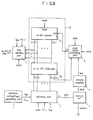
- Fig: 3 illustrates a block diagram of a device for sensing a data in a multibit memory cell in accordance with a first embodiment of the present invention.
- the device for sensing a data in a multibit memory cell in accordance with a first embodiment of the present invention includes a reference voltage generating part 1 for generating a plurality of reference voltages(2 n -1 in case of n bits), a switching part 2 for applying the plurality of reference voltages from the reference voltage generating part 1 to a control gate in a memory cell 3 in succession under the control of the controlling part which will be explained later, a sensing part 4 for comparing the data recorded in the memory cell 3 having one of the reference voltage applied thereto to a reference value, a clock signal controlling part 5 for receiving a signal from the sensing part 4 and a highest voltage selection signal from a controlling part which will be explained below and subjecting to logical operation in controlling an external main clock signal, a controlling part 6 for applying a reference voltage selection signal to the switching part 2 to control the reference voltages generated in succession(in the order of from a lower reference voltage to a higher reference voltage or vice versa) and producing a data in response to
- the controlling part 6 includes a ring counter 8 for counting the clock signal from the clock signal controlling part 5 in generating the reference signal selection signals P 0 , P 1 --- P n-2 , and P n-1 , and an n-bit counter 9 for counting the clock signal from the clock signal controlling part 5 in producing a relevant data.
- Fig. 4 illustrates a detail circuit of a first embodiment of the switching part shown in Fig. 3
- Fig. 5 illustrates a detail circuit of a second embodiment of the switching part shown in Fig. 3
- Fig. 6 illustrates a detail circuit of the clock signal controlling part shown in Fig. 3
- Fig. 7 illustrates a detail circuit of the latching part shown in Fig. 3.
- the switching part 1 includes a plurality of transistors M 1 , M 2 , ---, M n-1 each for switching the plurality of reference voltages from the reference voltage generating part 1 in succession in response to the reference voltage selection signals P 0 , P 1 , P 2 , --- and P n-2 except the highest reference voltage selection signal P n-1 of the reference voltage selection signals P 0 , , P 1 --- P n-2 , and P n-1 from the controlling part 6, an OR gate IC 1 for subjecting the highest reference voltage selection signal P n-1 from the controlling part 6, a signal S OUT from the sensing part 4 and a reset signal RESET to a logical sum operation, and a transistor Q 1 for switching the reference voltages applied to an output terminal thereof from the plurality of transistors M 1 , M 2 , ---, M n-1 in response to a signal from the OR gate IC 1 .
- the switching part 2 may include a plurality of pass transistors PTR 1 as shown in Fig. 5 in place of the plurality of transistors M 1 , M 2 , ---, M n-1 shown in Fig. 4, each of which produces the reference signal at "high".
- the clock signal controlling part 5 includes an NOR gate IC 2 for subjecting the highest reference voltage selection signal P n-1 from the controlling part 6 and the signal S OUT from the sensing part 4 to a logical sum operation and inverting a resultant of the logical sum operation, and an AND gate IC 3 for subjecting a start signal START, external main clock signal CLOCK and a signal from the NOR gate IC 2 to a logical production operation in applying the clock signal to the controlling part 6.
- the latching part 7 includes a plurality of flipflops. That is, the latching part 7 includes a delay D 1 for delaying the highest reference voltage selection signal P n-1 for a predetermined time period, an OR gate IC 4 for subjecting a signal from the delay D 1 and the signal S OUT from the sensing part 4 to a logical sum operation, and the plurality of flipflops F/F 0 , F/F 1 , ---, F/F n-1 for latching the data from the n-bit counter 9 in the controlling part 6 using a signal from the OR gate IC 4 as a clock signal.
- Fig. 8 illustrates a block diagram of a device for sensing a data in a multibit memory cell in accordance with a second embodiment of the present invention.
- the device for sensing a data in a multibit memory cell in accordance with a second embodiment of the present invention has a decoder 8a for decoding the plurality of reference signal selection signals in place of the ring counter 8 in the controlling part 6 of the device for sensing a data in a multibit memory cell in accordance with the first embodiment of the present invention.
- a sensing method in the device for sensing a data in a multibit memory cell in accordance with the present invention will be explained.
- Fig. 9 explains threshold levels of an n bit cell and the corresponding reference voltages in accordance with the present invention
- Fig. 10 explains reference voltage selection in the first embodiment of the present invention
- Fig. 11 explains reference voltage selection in the second embodiment of the present invention.
- a value between adjacent threshold levels is taken as the reference voltage.
- the reference voltage generating part 1 generates 2 n -1 number of voltages each corresponding to an intermediate value of adjacent threshold voltage levels in case of an n bit memory cell.
- the controlling part 6 controls the switching part 2 to output the reference voltages from the reference voltage generating part 1 in succession.
- the threshold levels are n bits, though a 2 n -1 number of reference voltages is required, a number of the reference voltage selection signals from the controlling part 6 is 2 n .
- the reference voltages are actually selected by the reference voltage selection signals P 0 , P 1 , P 2 , --- and P n-2 , but the highest reference voltage selection signal P n-1 . That is, the controlling part 6 controls the switching part 2 to output the reference voltages in an order of from a lower voltage to a higher voltage as shown in Fig. 10, or from a higher voltage to a lower voltage as shown in Fig. 11, by the following method.
- the transistors M 1 , M 2 , ---, M n-1 in the switching part 2 having the high signals applied thereto are turned on to output the reference voltages in the order of from a lower voltage to a higher voltage as shown in Fig. 10.
- the highest reference voltage selection signal P n-1 is applied, not to any of the transistors in the switching part 2, but to the OR gate IC 1 in the switching part 2, clock signal controlling part 5 and the latching part 7.
- the highest reference voltage is produced by the reference voltage selection signal P n-2 .
- the transistors M 1 , M 2 , ---, M n-1 in the switching part 2 having the high signals applied thereto are turned on to output the reference voltages in the order of from a higher voltage to a lower voltage as shown in Fig. 11.
- the reference voltages in the order of from lower reference voltage to higher reference voltage as shown in Fig. 10, because, at reading data, the data may be sensed, not always by selecting up to the last reference voltage, but by selecting an intermediate reference voltage.
- the sensing part makes turning on/off operations.
- a channel is formed between a source region and a drain region in the memory cell 3 in case a reference voltage over a threshold level is applied to the control gate, and no channel is formed between the source region and the drain region in the memory cell 3 in case a reference voltage below a threshold level is applied to the control gate.
- the sensing part 4 also produces a high signal when a reference voltage over a threshold level is applied to the control gate, and a low signal when a reference voltage below a threshold level is applied to the control gate.
- the controlling part 6 applies the reference voltages to the control gate on the memory cell 3 in the order of from lower reference voltage to higher reference voltage as shown in Fig. 10, the memory cell has been programmed in one of the two bit threshold levels V TH, 0 , V TH, 1 , V TH, 2 and V TH, 3 , and there are three of the reference voltages V REF, 0 , V REF, 1 and V REF, 2 each of which value falls on between adjacent two of the threshold levels.
- the sensing part 4 Upon the reference voltage V REF,0 a is applied to the control gate on the memory cell 3 by the switching part 2, the sensing part 4 produces a high signal only when the memory cell has been programmed in the threshold level V TH,0 because the channel will be formed between the source region and the drain region of the memory cell, and the sensing part 4 produces a low signal when the memory cell has been programmed in one of the rest of the threshold levels V TH, 1 , V TH, 2 and V TH, 3 .
- the sensing part 4 upon the reference voltage V REF, 2 is applied to the control gate on the memory cell 3 by the switching part 2, the sensing part 4 produces a low signal only when the memory cell has been-programmed in the threshold level V TH, 3 because the channel will not be formed between the source region and the drain region of the memory cell, and the sensing part 4 produces a high signal when the memory cell has been programmed in one of the rest of the threshold levels V TH,0 , V TH, 1 and V TH, 2 .
- the device of the present invention senses a data in the multibit memory cell.
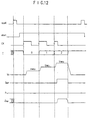
- FIG. 12 explains timings of different parts when the memory cell of the present invention is programmed in a threshold level V TH2
- Fig. 13 explains timings of different parts when the highest level data is read according to the present invention.
- the clock signal controlling part 5 Upon reception of an external main clock signal CLOCK, then, a reset signal RESET and a start signal START, the clock signal controlling part 5 produces a clock signal to the controlling part 6.
- the controlling part 6 then counts the clock to generates a reference voltage selection signal and a 2 bit data signal. That is, the ring counter 8 in the controlling part 6 causes the lowest reference voltage V REF, 0 a to be produced and applied to the memory cell 3 through the switching part 2, and the n bit counter 9 in the controlling part 6 produces a data 00.
- the sensing part 4 Upon reception of the reference voltage V REF, 0 a thus, since the memory cell 3 is programmed in the threshold level V TH,, 2 , the sensing part 4 produces a low signal.
- the NOR gate IC 2 in the clock signal controlling part 6 produces a high signal, so that the AND gate IC 3 in the clock signal controlling part 5 continues to apply the external main clock signal CLOCK to the controlling part 6.
- the controlling part 6 controls the ring counter 8 to produce the reference voltage selection signal P 1 at a second rising edge of the clock signal for producing the next reference voltage V REF, 1 , the reference voltage V REF,1 produced in the reference voltage generating part 1 to be applied to the memory cell 3, and the n bit counter 9 to produce the data 01. Even if the reference voltage V REF, 1 is received, the sensing part 4 produces a low signal because the memory cell 3 has been programmed in the threshold level V TH, 2 .
- the NOR gate IC 2 in the clock signal controlling part 6 produces a high signal, so that the AND gate IC 3 in the clock signal controlling part 5 continues to apply the external main clock signal CLOCK to the controlling part 6. Then, the controlling part 6 controls the ring counter 8 and the n bit counter 9 to cause the reference voltage V REF, 2 generated in the reference signal generating part 1 to be applied to the memory cell 3 through the switching part 2 and to produce the data 10 respectively at a third rising edge of the clock signal.
- the sensing part 4 Upon reception of the reference voltage V REF, 2 , the sensing part 4 produces a high signal because the memory cell 3 has been programmed in the threshold level V TH, 2 .
- the NOR gate IC 2 in the clock signal controlling part 5 produces a low signal regardless of the reference voltage selection signal P n-1 from the controlling part 6. Therefore, the AND gate IC 3 in the clock signal controlling part 5 applies no external main clock signal CLOCK to the controlling part 6. If no clock signal is applied to the controlling part 6, all the parts of the sensing device are initialized, and the latching part 7 presents the data 10 finally produced in the n bit counter 9 of the controlling part 6 as a sensed data.
- a 2 n -1 number of level values are sensed except the highest level value in the multilevel programmed memory cell, and the remained one highest level value is sensed by a method as shown in Fig. 13.
- the sensing part 4 produces a low signal.
- the clock signal controlling part 5 also continues to apply the external clock signal to the controlling part 6.
- the ring counter 8 and the n bit counter 9 in the controlling part 6 respectively count the clock signal to produce the highest reference voltage selection signal P n-1 at "high” and to apply the data 11 to the latching part 7 at a fourth rising edge of the clock signal, respectively.
- the NOR gate IC 2 in the clock signal controlling part 5 then produces a low signal to stop application of the external clock signal to the controlling part 6 even if the low signal is under production in the sensing part 4.
- the latching part 7 can present a final data 11.
- the sensing method of the device for sensing a data in a multibit memory cell in accordance with the second embodiment of the present invention is identical to the sensing method of the device for sensing a data in a multibit memory cell in accordance with the first embodiment of the present invention, except the operation of the controlling part 6. That is, the decoder 8a in the second embodiment is applied of, not the clock signal from the clock signal controlling part 5, but the a data signal from the n bit counter 9, in decoding the reference voltage selection signal.
- the data sensing device and method for a multibit memory cell of the present invention has the following advantages.
- the requirement for application of only one reference voltage of a certain value to the sensing amplifier helps to reduce a power consumption
Landscapes
- Engineering & Computer Science (AREA)
- Computer Hardware Design (AREA)
- Read Only Memory (AREA)
- Static Random-Access Memory (AREA)
Applications Claiming Priority (2)
| Application Number | Priority Date | Filing Date | Title |
|---|---|---|---|
| KR9676873 | 1996-12-30 | ||
| KR1019960076873A KR100226746B1 (ko) | 1996-12-30 | 1996-12-30 | 다중비트셀의데이타센싱장치및방법 |
Publications (3)
| Publication Number | Publication Date |
|---|---|
| EP0851429A2 true EP0851429A2 (fr) | 1998-07-01 |
| EP0851429A3 EP0851429A3 (fr) | 1999-03-31 |
| EP0851429B1 EP0851429B1 (fr) | 2003-12-17 |
Family
ID=19492355
Family Applications (1)
| Application Number | Title | Priority Date | Filing Date |
|---|---|---|---|
| EP97109419A Expired - Lifetime EP0851429B1 (fr) | 1996-12-30 | 1997-06-10 | Dispositif de détection de données et méthode pour cellule de mémoire multibit |
Country Status (6)
| Country | Link |
|---|---|
| US (1) | US5943259A (fr) |
| EP (1) | EP0851429B1 (fr) |
| JP (1) | JP3722401B2 (fr) |
| KR (1) | KR100226746B1 (fr) |
| CN (1) | CN1124608C (fr) |
| DE (1) | DE69726832T2 (fr) |
Cited By (2)
| Publication number | Priority date | Publication date | Assignee | Title |
|---|---|---|---|---|
| EP1068620A4 (fr) * | 1998-04-01 | 2001-04-18 | Invox Technology | Memoire haute definition a bits multiples par cellule |
| WO2012017844A1 (fr) * | 2010-08-06 | 2012-02-09 | Semiconductor Energy Laboratory Co., Ltd. | Dispositif à semi-conducteur |
Families Citing this family (15)
| Publication number | Priority date | Publication date | Assignee | Title |
|---|---|---|---|---|
| US6222762B1 (en) | 1992-01-14 | 2001-04-24 | Sandisk Corporation | Multi-state memory |
| US6137739A (en) * | 1998-06-29 | 2000-10-24 | Hyundai Electronics Industries Co., Ltd. | Multilevel sensing circuit and method thereof |
| KR100542397B1 (ko) * | 2000-12-29 | 2006-01-10 | 주식회사 하이닉스반도체 | 반도체 메모리 소자의 센싱 회로 |
| US6577161B2 (en) | 2001-06-01 | 2003-06-10 | Macronix International Co., Ltd. | One cell programmable switch using non-volatile cell with unidirectional and bidirectional states |
| US6531887B2 (en) | 2001-06-01 | 2003-03-11 | Macronix International Co., Ltd. | One cell programmable switch using non-volatile cell |
| US6545504B2 (en) * | 2001-06-01 | 2003-04-08 | Macronix International Co., Ltd. | Four state programmable interconnect device for bus line and I/O pad |
| US20050102573A1 (en) * | 2003-11-03 | 2005-05-12 | Macronix International Co., Ltd. | In-circuit configuration architecture for embedded configurable logic array |
| US20050097499A1 (en) * | 2003-11-03 | 2005-05-05 | Macronix International Co., Ltd. | In-circuit configuration architecture with non-volatile configuration store for embedded configurable logic array |
| JP2010140554A (ja) * | 2008-12-11 | 2010-06-24 | Samsung Electronics Co Ltd | 不揮発性半導体記憶装置の読出し方法 |
| KR101056258B1 (ko) | 2009-09-14 | 2011-08-11 | 삼성모바일디스플레이주식회사 | 유기전계발광 표시장치 및 그의 구동방법 |
| US8427877B2 (en) * | 2011-02-11 | 2013-04-23 | Freescale Semiconductor, Inc. | Digital method to obtain the I-V curves of NVM bitcells |
| US9715924B2 (en) * | 2015-10-22 | 2017-07-25 | Sandisk Technologies Llc | Three dimensional non-volatile memory with current sensing programming status |
| CN112820225B (zh) * | 2019-11-15 | 2023-01-24 | 京东方科技集团股份有限公司 | 一种数据缓存电路、显示面板及显示装置 |
| TWI712040B (zh) * | 2020-05-12 | 2020-12-01 | 力旺電子股份有限公司 | 具多階型記憶胞陣列之非揮發性記憶體及其相關讀取控制方法 |
| JP7447317B2 (ja) * | 2021-02-09 | 2024-03-11 | 長江存儲科技有限責任公司 | 3次元メモリデバイスの読出し時間の改善 |
Family Cites Families (12)
| Publication number | Priority date | Publication date | Assignee | Title |
|---|---|---|---|---|
| US4331968A (en) * | 1980-03-17 | 1982-05-25 | Mostek Corporation | Three layer floating gate memory transistor with erase gate over field oxide region |
| US5043940A (en) * | 1988-06-08 | 1991-08-27 | Eliyahou Harari | Flash EEPROM memory systems having multistate storage cells |
| US5268318A (en) * | 1988-06-08 | 1993-12-07 | Eliyahou Harari | Highly compact EPROM and flash EEPROM devices |
| FR2635410B1 (fr) * | 1988-08-11 | 1991-08-02 | Sgs Thomson Microelectronics | Memoire de type eprom a haute densite d'integration avec une organisation en damier et un facteur de couplage ameliore et procede de fabrication |
| US5163021A (en) * | 1989-04-13 | 1992-11-10 | Sundisk Corporation | Multi-state EEprom read and write circuits and techniques |
| US5218569A (en) * | 1991-02-08 | 1993-06-08 | Banks Gerald J | Electrically alterable non-volatile memory with n-bits per memory cell |
| US5257220A (en) * | 1992-03-13 | 1993-10-26 | Research Foundation Of The State Univ. Of N.Y. | Digital data memory unit and memory unit array |
| US5422842A (en) * | 1993-07-08 | 1995-06-06 | Sundisk Corporation | Method and circuit for simultaneously programming and verifying the programming of selected EEPROM cells |
| JP3179943B2 (ja) * | 1993-07-12 | 2001-06-25 | 株式会社東芝 | 半導体記憶装置 |
| CN1147866C (zh) * | 1994-06-02 | 2004-04-28 | 英特尔公司 | 含多级单元的快擦存储器的读出电路 |
| US5508958A (en) * | 1994-09-29 | 1996-04-16 | Intel Corporation | Method and apparatus for sensing the state of floating gate memory cells by applying a variable gate voltage |
| US5687114A (en) * | 1995-10-06 | 1997-11-11 | Agate Semiconductor, Inc. | Integrated circuit for storage and retrieval of multiple digital bits per nonvolatile memory cell |
-
1996
- 1996-12-30 KR KR1019960076873A patent/KR100226746B1/ko not_active Expired - Fee Related
-
1997
- 1997-06-10 EP EP97109419A patent/EP0851429B1/fr not_active Expired - Lifetime
- 1997-06-10 DE DE69726832T patent/DE69726832T2/de not_active Expired - Lifetime
- 1997-07-16 CN CN97114680A patent/CN1124608C/zh not_active Expired - Fee Related
- 1997-12-08 JP JP33699897A patent/JP3722401B2/ja not_active Expired - Fee Related
- 1997-12-30 US US09/000,610 patent/US5943259A/en not_active Expired - Lifetime
Cited By (7)
| Publication number | Priority date | Publication date | Assignee | Title |
|---|---|---|---|---|
| EP1068620A4 (fr) * | 1998-04-01 | 2001-04-18 | Invox Technology | Memoire haute definition a bits multiples par cellule |
| WO2012017844A1 (fr) * | 2010-08-06 | 2012-02-09 | Semiconductor Energy Laboratory Co., Ltd. | Dispositif à semi-conducteur |
| CN103026416A (zh) * | 2010-08-06 | 2013-04-03 | 株式会社半导体能源研究所 | 半导体装置 |
| US8488394B2 (en) | 2010-08-06 | 2013-07-16 | Semiconductor Energy Laboratory Co., Ltd. | Semiconductor device |
| US8837232B2 (en) | 2010-08-06 | 2014-09-16 | Semiconductor Energy Laboratory Co., Ltd. | Semiconductor device |
| CN103026416B (zh) * | 2010-08-06 | 2016-04-27 | 株式会社半导体能源研究所 | 半导体装置 |
| TWI549131B (zh) * | 2010-08-06 | 2016-09-11 | 半導體能源研究所股份有限公司 | 半導體裝置 |
Also Published As
| Publication number | Publication date |
|---|---|
| DE69726832D1 (de) | 2004-01-29 |
| EP0851429A3 (fr) | 1999-03-31 |
| JPH10199269A (ja) | 1998-07-31 |
| CN1124608C (zh) | 2003-10-15 |
| CN1187010A (zh) | 1998-07-08 |
| DE69726832T2 (de) | 2004-11-04 |
| US5943259A (en) | 1999-08-24 |
| JP3722401B2 (ja) | 2005-11-30 |
| EP0851429B1 (fr) | 2003-12-17 |
| KR19980057576A (ko) | 1998-09-25 |
| KR100226746B1 (ko) | 1999-10-15 |
Similar Documents
| Publication | Publication Date | Title |
|---|---|---|
| US5539690A (en) | Write verify schemes for flash memory with multilevel cells | |
| EP0851429B1 (fr) | Dispositif de détection de données et méthode pour cellule de mémoire multibit | |
| US6961266B2 (en) | Method of programming/reading multi-level flash memory using sensing circuit | |
| US6097637A (en) | Dynamic single bit per cell to multiple bit per cell memory | |
| US6327189B2 (en) | Electrically alterable non-volatile memory with n-bits per cell | |
| EP1467377B1 (fr) | Methode de lecture d'une mémoire non-volatile et dispositif associé | |
| EP1620860B1 (fr) | Memoire a seuil de lecture et de verification homogene | |
| US6655758B2 (en) | Method for storing data in a nonvolatile memory | |
| US20020101778A1 (en) | Integrated circuit for storage and retrieval of multiple digital bits per nonvolatile memory cell | |
| KR19990063059A (ko) | 불휘발성 반도체 기억장치 및 이를 사용한 ic 메모리 카드 | |
| EP0740305B1 (fr) | Dispositif de mémoire morte ultra rapide à multi-états | |
| US6178114B1 (en) | Sensing apparatus and method for fetching multi-level cell data | |
| US5790454A (en) | Data sensing apparatus and method of multi-bit memory cell | |
| US6735121B2 (en) | Nonvolatile memory system having status register for rewrite control | |
| US5751632A (en) | Device for and method of sensing data of multi-bit memory cell | |
| US7551503B2 (en) | Method for refreshing a flash memory | |
| US7483324B2 (en) | Memory device and method providing an average threshold based refresh mechanism | |
| US6026049A (en) | Semiconductor memory with sensing stability | |
| JP2000215685A (ja) | メモリアレイのマルチビットメモリセル用検知回路及び検知方法 |
Legal Events
| Date | Code | Title | Description |
|---|---|---|---|
| PUAI | Public reference made under article 153(3) epc to a published international application that has entered the european phase |
Free format text: ORIGINAL CODE: 0009012 |
|
| 17P | Request for examination filed |
Effective date: 19970610 |
|
| AK | Designated contracting states |
Kind code of ref document: A2 Designated state(s): DE FR GB NL |
|
| PUAL | Search report despatched |
Free format text: ORIGINAL CODE: 0009013 |
|
| AK | Designated contracting states |
Kind code of ref document: A3 Designated state(s): AT BE CH DE DK ES FI FR GB GR IE IT LI LU MC NL PT SE |
|
| AKX | Designation fees paid |
Free format text: DE FR GB NL |
|
| 17Q | First examination report despatched |
Effective date: 20020514 |
|
| GRAH | Despatch of communication of intention to grant a patent |
Free format text: ORIGINAL CODE: EPIDOS IGRA |
|
| GRAS | Grant fee paid |
Free format text: ORIGINAL CODE: EPIDOSNIGR3 |
|
| GRAA | (expected) grant |
Free format text: ORIGINAL CODE: 0009210 |
|
| AK | Designated contracting states |
Kind code of ref document: B1 Designated state(s): DE FR GB NL |
|
| REG | Reference to a national code |
Ref country code: GB Ref legal event code: FG4D |
|
| REF | Corresponds to: |
Ref document number: 69726832 Country of ref document: DE Date of ref document: 20040129 Kind code of ref document: P |
|
| ET | Fr: translation filed | ||
| PLBE | No opposition filed within time limit |
Free format text: ORIGINAL CODE: 0009261 |
|
| STAA | Information on the status of an ep patent application or granted ep patent |
Free format text: STATUS: NO OPPOSITION FILED WITHIN TIME LIMIT |
|
| 26N | No opposition filed |
Effective date: 20040920 |
|
| PGFP | Annual fee paid to national office [announced via postgrant information from national office to epo] |
Ref country code: DE Payment date: 20120531 Year of fee payment: 16 Ref country code: NL Payment date: 20120530 Year of fee payment: 16 |
|
| PGFP | Annual fee paid to national office [announced via postgrant information from national office to epo] |
Ref country code: FR Payment date: 20120618 Year of fee payment: 16 Ref country code: GB Payment date: 20120530 Year of fee payment: 16 |
|
| REG | Reference to a national code |
Ref country code: NL Ref legal event code: V1 Effective date: 20140101 |
|
| GBPC | Gb: european patent ceased through non-payment of renewal fee |
Effective date: 20130610 |
|
| REG | Reference to a national code |
Ref country code: DE Ref legal event code: R119 Ref document number: 69726832 Country of ref document: DE Effective date: 20140101 |
|
| REG | Reference to a national code |
Ref country code: FR Ref legal event code: ST Effective date: 20140228 |
|
| PG25 | Lapsed in a contracting state [announced via postgrant information from national office to epo] |
Ref country code: GB Free format text: LAPSE BECAUSE OF NON-PAYMENT OF DUE FEES Effective date: 20130610 Ref country code: NL Free format text: LAPSE BECAUSE OF NON-PAYMENT OF DUE FEES Effective date: 20140101 Ref country code: DE Free format text: LAPSE BECAUSE OF NON-PAYMENT OF DUE FEES Effective date: 20140101 |
|
| PG25 | Lapsed in a contracting state [announced via postgrant information from national office to epo] |
Ref country code: FR Free format text: LAPSE BECAUSE OF NON-PAYMENT OF DUE FEES Effective date: 20130701 |