EP0851477A2 - Verfahren zur Kontrolle der Genauigkeit beim mehrstufigen Ätzen - Google Patents
Verfahren zur Kontrolle der Genauigkeit beim mehrstufigen Ätzen Download PDFInfo
- Publication number
- EP0851477A2 EP0851477A2 EP97440136A EP97440136A EP0851477A2 EP 0851477 A2 EP0851477 A2 EP 0851477A2 EP 97440136 A EP97440136 A EP 97440136A EP 97440136 A EP97440136 A EP 97440136A EP 0851477 A2 EP0851477 A2 EP 0851477A2
- Authority
- EP
- European Patent Office
- Prior art keywords
- etching
- substrate
- accuracy
- different
- masks
- Prior art date
- Legal status (The legal status is an assumption and is not a legal conclusion. Google has not performed a legal analysis and makes no representation as to the accuracy of the status listed.)
- Withdrawn
Links
- 238000005530 etching Methods 0.000 title claims abstract description 32
- 238000000034 method Methods 0.000 title claims abstract description 17
- 239000000758 substrate Substances 0.000 claims abstract description 14
- 238000004519 manufacturing process Methods 0.000 claims abstract description 5
- 238000003754 machining Methods 0.000 claims description 3
- 238000012544 monitoring process Methods 0.000 abstract 1
- 230000005693 optoelectronics Effects 0.000 description 1
- 229910052710 silicon Inorganic materials 0.000 description 1
- 239000010703 silicon Substances 0.000 description 1
Images
Classifications
-
- C—CHEMISTRY; METALLURGY
- C23—COATING METALLIC MATERIAL; COATING MATERIAL WITH METALLIC MATERIAL; CHEMICAL SURFACE TREATMENT; DIFFUSION TREATMENT OF METALLIC MATERIAL; COATING BY VACUUM EVAPORATION, BY SPUTTERING, BY ION IMPLANTATION OR BY CHEMICAL VAPOUR DEPOSITION, IN GENERAL; INHIBITING CORROSION OF METALLIC MATERIAL OR INCRUSTATION IN GENERAL
- C23F—NON-MECHANICAL REMOVAL OF METALLIC MATERIAL FROM SURFACE; INHIBITING CORROSION OF METALLIC MATERIAL OR INCRUSTATION IN GENERAL; MULTI-STEP PROCESSES FOR SURFACE TREATMENT OF METALLIC MATERIAL INVOLVING AT LEAST ONE PROCESS PROVIDED FOR IN CLASS C23 AND AT LEAST ONE PROCESS COVERED BY SUBCLASS C21D OR C22F OR CLASS C25
- C23F1/00—Etching metallic material by chemical means
-
- G—PHYSICS
- G03—PHOTOGRAPHY; CINEMATOGRAPHY; ANALOGOUS TECHNIQUES USING WAVES OTHER THAN OPTICAL WAVES; ELECTROGRAPHY; HOLOGRAPHY
- G03F—PHOTOMECHANICAL PRODUCTION OF TEXTURED OR PATTERNED SURFACES, e.g. FOR PRINTING, FOR PROCESSING OF SEMICONDUCTOR DEVICES; MATERIALS THEREFOR; ORIGINALS THEREFOR; APPARATUS SPECIALLY ADAPTED THEREFOR
- G03F7/00—Photomechanical, e.g. photolithographic, production of textured or patterned surfaces, e.g. printing surfaces; Materials therefor, e.g. comprising photoresists; Apparatus specially adapted therefor
- G03F7/70—Microphotolithographic exposure; Apparatus therefor
- G03F7/70483—Information management; Active and passive control; Testing; Wafer monitoring, e.g. pattern monitoring
- G03F7/70605—Workpiece metrology
- G03F7/70616—Monitoring the printed patterns
- G03F7/70633—Overlay, i.e. relative alignment between patterns printed by separate exposures in different layers, or in the same layer in multiple exposures or stitching
-
- Y—GENERAL TAGGING OF NEW TECHNOLOGICAL DEVELOPMENTS; GENERAL TAGGING OF CROSS-SECTIONAL TECHNOLOGIES SPANNING OVER SEVERAL SECTIONS OF THE IPC; TECHNICAL SUBJECTS COVERED BY FORMER USPC CROSS-REFERENCE ART COLLECTIONS [XRACs] AND DIGESTS
- Y10—TECHNICAL SUBJECTS COVERED BY FORMER USPC
- Y10T—TECHNICAL SUBJECTS COVERED BY FORMER US CLASSIFICATION
- Y10T428/00—Stock material or miscellaneous articles
- Y10T428/24—Structurally defined web or sheet [e.g., overall dimension, etc.]
- Y10T428/24479—Structurally defined web or sheet [e.g., overall dimension, etc.] including variation in thickness
-
- Y—GENERAL TAGGING OF NEW TECHNOLOGICAL DEVELOPMENTS; GENERAL TAGGING OF CROSS-SECTIONAL TECHNOLOGIES SPANNING OVER SEVERAL SECTIONS OF THE IPC; TECHNICAL SUBJECTS COVERED BY FORMER USPC CROSS-REFERENCE ART COLLECTIONS [XRACs] AND DIGESTS
- Y10—TECHNICAL SUBJECTS COVERED BY FORMER USPC
- Y10T—TECHNICAL SUBJECTS COVERED BY FORMER US CLASSIFICATION
- Y10T428/00—Stock material or miscellaneous articles
- Y10T428/24—Structurally defined web or sheet [e.g., overall dimension, etc.]
- Y10T428/24479—Structurally defined web or sheet [e.g., overall dimension, etc.] including variation in thickness
- Y10T428/2457—Parallel ribs and/or grooves
Definitions
- the invention relates to a method for checking the accuracy of the machining result in the production of depressions in a substrate through multi-stage etching.
- Components that have high-precision microstructures are made by Etching. To do this, it is necessary that they follow a photolithographic Process can be provided with etching masks. If the microstructures have a complicated shape, i.e. they different Have structure depths and are also nested, then two or more etching processes must be carried out.
- the technical problem underlying the invention is a Provide means to easily check whether the high-precision microstructure after the multi-stage etching process has the required accuracy.
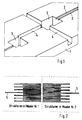
- Fig. 1 the section of a substrate 1 can be seen, in which by Etch recesses of different shapes and depths have been generated. It is the relatively flat channels 2 that box-shaped depressions 3 and the trenches 4 can be seen.
- substrates are used as a micro-optical assembly bench at Manufacture of optoelectronic components used.
- the substrate consists of silicon.
- the invention but can be used in the manufacture of other items through multi-stage Etching can be used to check the quality of the machining. It is known that a large number of precision components are formed by form etching produced.
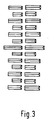
- the divisions of the Line pattern for example, a distance of 40 microns (1st mask) or 40.5 ⁇ m (2nd mask).
- the width of the lines is 20 ⁇ m and their Lengths are 50.75 and 100 ⁇ m.
Landscapes
- Chemical & Material Sciences (AREA)
- Physics & Mathematics (AREA)
- General Physics & Mathematics (AREA)
- Engineering & Computer Science (AREA)
- Materials Engineering (AREA)
- Mechanical Engineering (AREA)
- Metallurgy (AREA)
- Organic Chemistry (AREA)
- Chemical Kinetics & Catalysis (AREA)
- General Chemical & Material Sciences (AREA)
- Weting (AREA)
- ing And Chemical Polishing (AREA)
- Length-Measuring Instruments Using Mechanical Means (AREA)
- Length Measuring Devices With Unspecified Measuring Means (AREA)
- Drying Of Semiconductors (AREA)
- Preparing Plates And Mask In Photomechanical Process (AREA)
- Exposure And Positioning Against Photoresist Photosensitive Materials (AREA)
- Exposure Of Semiconductors, Excluding Electron Or Ion Beam Exposure (AREA)
- Micromachines (AREA)
Abstract
Description
- Fig. 1
- den Ausschnitt aus einem in einem zweistufigen Ätzvorgang hergestellten Substrat,
- Fig. 2
- die auf den beiden Ätzmasken verwendeten Strichmuster und
- Fig. 3
- die von den Ätzmasken auf dem Substrat erzeugten geätzten Strichmuster.
Claims (2)
- Verfahren zur Kontrolle der Genauigkeit des Bearbeitungsergebnisses bei der Herstellung von Vertiefungen in einem Substrat durch mehrstufiges Ätzen, dadurch gekennzeichnet, daß auf den Ätzmasken ein Strichmuster angebracht ist und sich die Strichmuster auf den Ätzmasken für verschiedene Ätzstufen derart unterscheiden, daß sie ein Noniussystem bilden.
- Durch mehrstufiges Ätzen mit Vertiefungen versehenes Substrat, dadurch gekennzeichnet, daß auf ihm mehrere geätzte Strichmuster vorhanden sind.
Applications Claiming Priority (2)
| Application Number | Priority Date | Filing Date | Title |
|---|---|---|---|
| DE19652974 | 1996-12-19 | ||
| DE19652974A DE19652974A1 (de) | 1996-12-19 | 1996-12-19 | Verfahren zur Kontrolle der Genauigkeit beim mehrstufigen Ätzen |
Publications (2)
| Publication Number | Publication Date |
|---|---|
| EP0851477A2 true EP0851477A2 (de) | 1998-07-01 |
| EP0851477A3 EP0851477A3 (de) | 1999-02-10 |
Family
ID=7815332
Family Applications (1)
| Application Number | Title | Priority Date | Filing Date |
|---|---|---|---|
| EP97440136A Withdrawn EP0851477A3 (de) | 1996-12-19 | 1997-12-17 | Verfahren zur Kontrolle der Genauigkeit beim mehrstufigen Ätzen |
Country Status (4)
| Country | Link |
|---|---|
| US (2) | US6077449A (de) |
| EP (1) | EP0851477A3 (de) |
| JP (1) | JPH10300402A (de) |
| DE (1) | DE19652974A1 (de) |
Family Cites Families (11)
| Publication number | Priority date | Publication date | Assignee | Title |
|---|---|---|---|---|
| DE152365C (de) * | ||||
| DE243537C (de) * | 1910-06-01 | 1912-02-14 | ||
| US1881803A (en) * | 1928-02-15 | 1932-10-11 | Ambler Asbestos Shingle & Shea | Ornamental product and method of producing same |
| GB1085164A (en) * | 1965-12-28 | 1967-09-27 | Buckbee Mears Co | Automatically controlling the size of holes etched in continuous metal webs |
| DE2226149A1 (de) * | 1971-11-02 | 1973-05-10 | Halbleiterwerk Frankfurt Oder | Verfahren zum erkennen der groesse von lage-, winkel- und ueberdeckungsfehlern bei der herstellung und anwendung von schablonen in der halbleitertechnik |
| US4529314A (en) * | 1980-04-18 | 1985-07-16 | Harris Corporation | Method of measuring misalignment between levels on a substrate |
| DD152365A5 (de) * | 1980-07-30 | 1981-11-25 | Rca Corp | Verfahren zur praezisionsaetzung einer laufenden folge von artikeln |
| US4814213A (en) * | 1987-07-20 | 1989-03-21 | Therma-Tru Corp. | Bevelled glass assembly |
| JP2666859B2 (ja) * | 1988-11-25 | 1997-10-22 | 日本電気株式会社 | 目合せ用バーニヤパターンを備えた半導体装置 |
| DE4341171C2 (de) * | 1993-12-02 | 1997-04-17 | Siemens Ag | Verfahren zur Herstellung einer integrierten Schaltungsanordnung |
| KR0170909B1 (ko) * | 1995-09-27 | 1999-03-30 | 김주용 | 반도체 소자의 오버레이 검사방법 |
-
1996
- 1996-12-19 DE DE19652974A patent/DE19652974A1/de not_active Withdrawn
-
1997
- 1997-12-16 US US08/991,673 patent/US6077449A/en not_active Expired - Fee Related
- 1997-12-17 EP EP97440136A patent/EP0851477A3/de not_active Withdrawn
- 1997-12-19 JP JP9351398A patent/JPH10300402A/ja active Pending
-
2000
- 2000-04-04 US US09/542,678 patent/US6379778B1/en not_active Expired - Fee Related
Also Published As
| Publication number | Publication date |
|---|---|
| EP0851477A3 (de) | 1999-02-10 |
| US6077449A (en) | 2000-06-20 |
| JPH10300402A (ja) | 1998-11-13 |
| US6379778B1 (en) | 2002-04-30 |
| DE19652974A1 (de) | 1998-06-25 |
Similar Documents
| Publication | Publication Date | Title |
|---|---|---|
| DE2721720C2 (de) | Präzisions-Meßwandler für Positionsmessungen | |
| DE4134291C2 (de) | ||
| EP0116674B1 (de) | Verfahren zur Herstellung einer Meisterplatte | |
| DE3225216C2 (de) | ||
| DE3586501T2 (de) | Herstellung und evaluation einer ausrichtung mittels ausrichtzeichen. | |
| EP0105189B1 (de) | Verfahren zum Herstellen von Metallelektroden unterschiedlicher Dicke für Halbleiterbauelemente, insbesondere für Leistungshalbleiterbauelemente wie Thyristoren | |
| DE19609399C2 (de) | Verfahren zum Bestimmen der Kristallorientierung in einem Wafer | |
| EP0851477A2 (de) | Verfahren zur Kontrolle der Genauigkeit beim mehrstufigen Ätzen | |
| EP0217071B1 (de) | Verfahren zur Erzeugung von Strukturen in der Mikromechanik | |
| EP0638924A1 (de) | Verfahren zum Herstellen von TAB-Filmträgern | |
| DE10001480B4 (de) | Verfahren zum Herstellen eines hochpräzisen Mehrscheiben-Schleifmodules und nach diesem Verfahren hergestelltes Mehrscheiben-Schleifmodul | |
| WO1999034421A1 (de) | Verfahren zur herstellung einer porösen schicht mit hilfe eines elektrochemischen ätzprozesses | |
| DE19805875C1 (de) | Trägertisch für eine Photomaske in einer Vorrichtung zur Mikrochip-Herstellung | |
| EP0498236A2 (de) | Verfahren zur Herstellung von Laserkreisel-Resonatorblöcken | |
| DE19512245A1 (de) | Photomaske zum Messen der Auflösung von Belichtungseinrichtungen | |
| DE4033233A1 (de) | Verfahren zur herstellung eines mikrostrukturkoerpers, insbesondere eines mikrostrukturierten abformwerkzeugs | |
| EP0674228A1 (de) | Lithografisches Verfahren | |
| DE19609202B4 (de) | Photomaske zur Strukturierung einer Supraleiterschicht, Supraleiterschicht und Verfahren zur Bestimmung des Ausmaßes einer Unterätzung bei der Strukturierung einer Supraleiterschicht | |
| DE19630739C1 (de) | Verfahren zum Herstellen einer Maske für Laserstrahlung | |
| WO2000017095A1 (de) | Kontrollstruktur zur herstellung von hohlräumen oder unterätzungsbereichen in mikromechanischen und/oder mikroelektronischen bauelementen | |
| DD262941A1 (de) | Duennschichtschaltkreis und verfahren zur strukturierung eines duennschichtschaltkreises | |
| DE4202039C2 (de) | Verfahren zur Herstellung optoelektronischer Bauelemente | |
| DE3336901C2 (de) | ||
| EP1308242A1 (de) | Bearbeitung von inhomogenen Materialien | |
| DE3015572A1 (de) | Verfahren zum maskieren mit hilfe von photolackbeschichtungen |
Legal Events
| Date | Code | Title | Description |
|---|---|---|---|
| PUAI | Public reference made under article 153(3) epc to a published international application that has entered the european phase |
Free format text: ORIGINAL CODE: 0009012 |
|
| AK | Designated contracting states |
Kind code of ref document: A2 Designated state(s): DE ES FR GB IT NL SE |
|
| AX | Request for extension of the european patent |
Free format text: AL;LT;LV;MK;RO;SI |
|
| PUAL | Search report despatched |
Free format text: ORIGINAL CODE: 0009013 |
|
| AK | Designated contracting states |
Kind code of ref document: A3 Designated state(s): AT BE CH DE DK ES FI FR GB GR IE IT LI LU MC NL PT SE |
|
| AX | Request for extension of the european patent |
Free format text: AL;LT;LV;MK;RO;SI |
|
| RAP3 | Party data changed (applicant data changed or rights of an application transferred) |
Owner name: ALCATEL |
|
| RAP3 | Party data changed (applicant data changed or rights of an application transferred) |
Owner name: ALCATEL |
|
| 17P | Request for examination filed |
Effective date: 19990611 |
|
| AKX | Designation fees paid |
Free format text: DE ES FR GB IT NL SE |
|
| STAA | Information on the status of an ep patent application or granted ep patent |
Free format text: STATUS: THE APPLICATION IS DEEMED TO BE WITHDRAWN |
|
| 18D | Application deemed to be withdrawn |
Effective date: 20040701 |