EP0851493A1 - Kontaktstruktur für elektronische EPROM oder flash EPROM Halbleiterschaltungen und ihr Herstellungsverfahren - Google Patents
Kontaktstruktur für elektronische EPROM oder flash EPROM Halbleiterschaltungen und ihr Herstellungsverfahren Download PDFInfo
- Publication number
- EP0851493A1 EP0851493A1 EP96830655A EP96830655A EP0851493A1 EP 0851493 A1 EP0851493 A1 EP 0851493A1 EP 96830655 A EP96830655 A EP 96830655A EP 96830655 A EP96830655 A EP 96830655A EP 0851493 A1 EP0851493 A1 EP 0851493A1
- Authority
- EP
- European Patent Office
- Prior art keywords
- contact
- bit lines
- contacts
- accordance
- matrix
- Prior art date
- Legal status (The legal status is an assumption and is not a legal conclusion. Google has not performed a legal analysis and makes no representation as to the accuracy of the status listed.)
- Granted
Links
Images

Classifications
-
- H—ELECTRICITY
- H10—SEMICONDUCTOR DEVICES; ELECTRIC SOLID-STATE DEVICES NOT OTHERWISE PROVIDED FOR
- H10W—GENERIC PACKAGES, INTERCONNECTIONS, CONNECTORS OR OTHER CONSTRUCTIONAL DETAILS OF DEVICES COVERED BY CLASS H10
- H10W20/00—Interconnections in chips, wafers or substrates
- H10W20/01—Manufacture or treatment
- H10W20/031—Manufacture or treatment of conductive parts of the interconnections
- H10W20/069—Manufacture or treatment of conductive parts of the interconnections by forming self-aligned vias or self-aligned contact plugs
-
- H—ELECTRICITY
- H10—SEMICONDUCTOR DEVICES; ELECTRIC SOLID-STATE DEVICES NOT OTHERWISE PROVIDED FOR
- H10W—GENERIC PACKAGES, INTERCONNECTIONS, CONNECTORS OR OTHER CONSTRUCTIONAL DETAILS OF DEVICES COVERED BY CLASS H10
- H10W20/00—Interconnections in chips, wafers or substrates
- H10W20/01—Manufacture or treatment
- H10W20/031—Manufacture or treatment of conductive parts of the interconnections
Definitions
- the present invention relates to a contact structure and to an associated manufacturing process for contacts in semiconductor electronic devices and in particular EPROM and Flash EPROM memories.
- the present invention relates to a process for manufacturing contacts in semiconductor electronic devices and in particular in bit lines of non-volatile memories with cross-point structure comprising memory cell matrices in which the bit lines are parallel unbroken diffusion strips extending along a column of the matrix with the contacts being provided through associated contact apertures defined through a dielectric layer deposited over a contact region defined in a semiconductor substrate at one end of the bit lines.
- the semiconductor electronic devices of EPROM and Flash EPROM memories comprise a plurality of non-volatile memory cells organized in matrices, i.e. the cells are organized in rows termed 'word lines' and columns termed 'bit lines'.
- Each individual non-volatile memory cell comprises a MOS transistor in which the gate, which is located over the channel region, is floating, i.e. it presents a high impedance towards all the other terminals of the same cell and of the circuit in which the cell is inserted.
- the cell comprises also a second electrode, termed control gate, which is driven by appropriate control voltages.
- control gate a second electrode, termed control gate, which is driven by appropriate control voltages.
- the other electrodes of the transistor are the usual drain, source and body terminals.
- the floating gate Since the floating gate displays high impedance towards any other terminal of the cell, the charge stored therein can remain for an indefinite time even if the power supply of the circuit in which it is inserted is removed.
- the cell thus displays non-volatile memory characteristics.
- Memory cells can be erased by ultraviolet (UV) radiation in EPROM memories or by electrical erasing in EEPROM or Flash-EPROM memories.
- the memory cells have source/drain regions provided in the substrate with unbroken, parallel diffusion strips denominated bit lines which coincide substantially with the matrix columns.
- this function is provided by metallization strips which connect individual contacts formed in the drain regions of the cells belonging to the same column.
- a contactless matrix calls for the presence of a virtual ground circuitry for the reading and programming steps.
- the savings in circuitry surface area obtained from such a structure is considerable and results in a reduction of approximately one order of magnitude in the number of contacts to be created.
- bit lines are contacted alternately and with a predetermined periodicity and indeed the contacts are present only at the opposite ends of the bit lines and are provided in opposing contact regions which delimit the circuit area designed to house the memory cells.
- the N+ doped region is a region implanted on a type P- substrate and is subjected to a positive (>0) bias with respect to the ground biased substrate, if the contact were not contained with a good margin in the N+ region it could contact the P- substrate to give rise to a leakage current.
- the contact can be provided with preset dimensional tolerances which must be considered in relation to the possible dimensional tolerances of the N+ region to be contacted and in relation to possible misalignments between the contact and the N+ region.
- the prior art offers some solutions for avoiding shortcomings in the manufacturing of contacts in the virtual ground matrices.
- a first solution calls for provision of an N+ area having a 'head' portion with dimensions sufficiently greater than the surface area occupied by the contact.
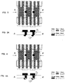
- FIGS 1 and 1A An example of this type of solution is shown in the annexed FIGS 1 and 1A.
- FIG 1 shows a plan view in enlarged scale of a detail of the layout of a portion 10 of an electronic memory circuit integrated on a semiconductor substrate 11. This portion 10 refers to the contact region at one end of the bit lines.
- active area strips 19 which could be replaced by pads provided only opposite the contact zone. Orthogonal to these strips 19 there are unbroken parallel diffusions of bit lines 12 provided by implantation and visible in FIG 1A.
- bit lines 12 are provided through parallel openings provided in this multilayer structure.
- FIG 1A although it is a cross section along plane of cut A-A' of FIG 1, does not correspond thereto from a temporal viewpoint but refers to the final steps of the manufacturing and contact creation process in the course of which the multilayer structure has already been removed from the contact region.
- a protective dielectric layer 13 which is subjected to a photolithographic process step followed by a chemical or plasma etching to define contact openings 14 opposite the bit lines 12.
- a contact 15 is provided within each of the openings 14 to allow establishment of an electrical connection between a bit line 12 and a corresponding metallization strip 16 deposited over the dielectric layer 13.
- FIG 1 shows parallel strips 17 of a first layer of polysilicon or Poly1 extending parallel to the bit lines and overlying the active area strips 19 in a direction orthogonal thereto. Opposite each contact 15 the strips 17 display a narrowing which confers a certain spacing to contact regions 18 in the center of which is provided a contact 15.
- This spacing entails essentially definition of a pad 18 sufficiently wide to allow provision by implantation of a type N+ region 12 having dimensions sufficiently greater than those of the contact 15.
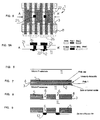
- a second solution proposed by the prior art requires that the contacts be realized by implantation contacting the N+ doped bit line through an appropriate opening. This solution is shown schematically in FIGS 2 to 4A and is particularly recommended when the lateral dimensions of the N+ region 12 do not ensure sufficient processing margin.
- FIG 2 shows clearly that the spacing between the polysilicon strips is constant and essentially as wide as the contact 15. Consequently the contact 15 must be provided by means of a self-aligned implantation step.
- this implantation allows providing a contact perfectly self-aligned with the corresponding active area as shown in FIG 2A.
- the technical problem underlying the present invention is to conceive a process for the provision of a contact structure and in particular for integrated memory circuits which would have functional characteristics providing direct contact with the corresponding active area even in situations where the area available for the contact is very small and saving a masking step.
- the solution idea underlying the present invention is that of utilizing an increase in the total width of the bit lines allowed by the implantation and subsequent diffusion of the N-channel selection transistor junctions associated with the memory cell matrix.
- reference number 1 indicates as a whole and schematically a circuit portion of a semiconductor substrate 11 comprising contact structures provided in accordance with the process of the present invention.
- the portion 1 is incorporated in an electronic memory circuit integrated on the semiconductor substrate 11 in accordance with a matrix architecture comprising a multiplicity of floating gate memory cells organized in rows and columns.
- this matrix is the EPROM or Flash-EPROM type with cross point structure and virtual ground circuitry e.g. as described in European patent No. 0 573 728 in which are provided unbroken parallel diffusion strips 12 termed bit lines aligned along the matrix columns.
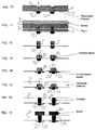
- FIG 6 shows the starting base of the manufacturing process of the semiconductor substrate 1 i.e. a semiconductor substrate 11 containing impurities of a first type of dopant, e.g. type P.
- the substrate 11 is prepared to receive the active areas of the memory cells and the selection transistors associated therewith through the formation of twin wells of the N-well and P-tub type in accordance with prior art procedures.
- the circuit portion 1 in which are provided the contact regions lying on a portion of substrate or on a type-P well adjacent to that which receives the memory cells. Indeed, as mentioned above, the contact regions are located at opposite ends of the bit lines.
- Preliminary steps of the manufacturing process call for an initial step of masking allowing definition on the substrate 11 of the active area regions.
- the active areas can be insulated from each other by insulating regions termed field oxide.
- another masking defines the regions in which are provided the cells by removing from the active area regions the gate oxide previously deposited. This step also allows performing an implantation of the channel region in order to adjust the threshold of the floating gate transistors which make up the memory cells.
- a multilayer structure comprising:
- a masking step denominated Poly1 masking allows defining openings 6 through which to provide the bit lines 12 of the memory cell matrix.
- the bit lines extend orthogonally in the substrate with respect to the active area regions.
- the openings 6 are opened by means of a cascaded etching step of the Poly Cap 5, the dielectric layer 4, the Poly1 layer 4 and the thin oxide 2 and if necessary the field oxide also where present. The etching continues until it brings to light the substrate 11 as shown in FIG 8.
- N+ ions e.g. arsenic ions
- arsenic ions An implantation of N+ ions, e.g. arsenic ions, is applied to provide the strips 12 of the bit lines of the memory matrix. If the memory cell matrix is the EPROM type the bit lines 12 are identical and provided only by the implantation of arsenic ions. The resulting structure is shown in FIG 9.
- alternating source and drain diffusions are provided by an implantation of arsenic + phosphorous and only arsenic respectively.
- This process step has the purpose of insulating the Poly1 walls which are designed to become the floating gates of the memory cells from a second polysilicon layer 8 which will be deposited subsequently.
- the manufacturing process also provides that the Poly Cap layer 5 and the interpoly dielectric be removed over the areas of the selection transistors and circuitry associated with the memory matrix. This process step is not illustrated in the FIGS because it is entirely conventional.
- a silicide layer 9 e.g. tungsten silicide as shown in FIG 11.
- This etching defines the memory matrix word lines. As concerns the contact region which is the object of the present invention it is necessary to expose a good part of the semiconductor 11. The result of this operation is shown in FIG 12 from which it is clear that the etching of the word lines does not entirely uncover the silicon in the contact region since the planarized dielectric plugs 7 remain to cover the N+ bit line diffusions 12.
- FIG 13 illustrates the creation of so-called spacers 20 behind the dielectric plugs 7.
- the spacers 20 are provided at the sides of the gate regions of the transistors of the outside circuitry but, because of the presence of the residual plugs 7, they also form behind the latter.
- the process continues with the provision by implantation and following diffusion of active N+ areas for the N-channel transistors and P+ active areas for the P-channel transistors making up part of the circuitry associated with the cell matrix.
- active N+ areas for the N-channel transistors and P+ active areas for the P-channel transistors making up part of the circuitry associated with the cell matrix.
- N+ regions 22 provided in the substrate 11 at the opposite sides of each bit line to be contacted thanks to the shielding offered by the residual dielectric plug 7. These regions 22 merge by diffusion with the bit line region 12 to create a single contact area sufficiently wide to receive the metallic contact even in case of misalignment of the latter with respect to the bit line.
- planarized dielectric layer 21 is deposited over the substrate 11 to cover the entire structure as shown in FIG 15.
- An appropriate contact masking defines the areas in which to provide contacts 25 through associated openings 24 made in the dielectric layer 21.
- the contacts 25 are provided by deposit of a metallization layer entirely occupying each opening 24 as shown in FIG 16.
- a following metal masking defines metallization areas 26 to which lead the contacts 25 as shown in FIG 17 which corresponds essentially to FIG 5A.
- the N+ implant is provided only outside the region protected by the residual plug 7 of planarized oxide.
- the N+ implantation occupies a region which extends beyond the oxide spacers 20 provided during formation of the LDD implants of the peripheral transistors.
Landscapes
- Semiconductor Memories (AREA)
- Electrodes Of Semiconductors (AREA)
- Non-Volatile Memory (AREA)
Priority Applications (4)
| Application Number | Priority Date | Filing Date | Title |
|---|---|---|---|
| EP96830655A EP0851493B9 (de) | 1996-12-27 | 1996-12-27 | Kontaktstruktur für elektronische EPROM oder flash EPROM Halbleiterschaltungen und ihr Herstellungsverfahren |
| DE69636738T DE69636738D1 (de) | 1996-12-27 | 1996-12-27 | Kontaktstruktur für elektronische EPROM oder flash EPROM Halbleiterschaltungen und ihr Herstellungsverfahren |
| JP9352533A JPH10275870A (ja) | 1996-12-27 | 1997-12-22 | Eprom又はフラッシュeprom半導体電子装置用のコンタクト構成体及びその製造方法 |
| US08/999,403 US6124169A (en) | 1996-12-27 | 1997-12-29 | Contact structure and associated process for production of semiconductor electronic devices and in particular nonvolatile EPROM and flash EPROM memories |
Applications Claiming Priority (1)
| Application Number | Priority Date | Filing Date | Title |
|---|---|---|---|
| EP96830655A EP0851493B9 (de) | 1996-12-27 | 1996-12-27 | Kontaktstruktur für elektronische EPROM oder flash EPROM Halbleiterschaltungen und ihr Herstellungsverfahren |
Publications (3)
| Publication Number | Publication Date |
|---|---|
| EP0851493A1 true EP0851493A1 (de) | 1998-07-01 |
| EP0851493B1 EP0851493B1 (de) | 2006-11-29 |
| EP0851493B9 EP0851493B9 (de) | 2007-09-12 |
Family
ID=8226096
Family Applications (1)
| Application Number | Title | Priority Date | Filing Date |
|---|---|---|---|
| EP96830655A Expired - Lifetime EP0851493B9 (de) | 1996-12-27 | 1996-12-27 | Kontaktstruktur für elektronische EPROM oder flash EPROM Halbleiterschaltungen und ihr Herstellungsverfahren |
Country Status (4)
| Country | Link |
|---|---|
| US (1) | US6124169A (de) |
| EP (1) | EP0851493B9 (de) |
| JP (1) | JPH10275870A (de) |
| DE (1) | DE69636738D1 (de) |
Families Citing this family (3)
| Publication number | Priority date | Publication date | Assignee | Title |
|---|---|---|---|---|
| TW556326B (en) * | 2001-05-30 | 2003-10-01 | Infineon Technologies Ag | A method for providing bitline contacts in a memory cell array and a memory cell array having bitline contacts |
| JP2003297957A (ja) * | 2002-04-05 | 2003-10-17 | Mitsubishi Electric Corp | 半導体装置及び半導体装置の製造方法 |
| KR102178732B1 (ko) * | 2013-12-20 | 2020-11-13 | 삼성전자주식회사 | 반도체 소자 |
Citations (3)
| Publication number | Priority date | Publication date | Assignee | Title |
|---|---|---|---|---|
| US4512073A (en) * | 1984-02-23 | 1985-04-23 | Rca Corporation | Method of forming self-aligned contact openings |
| JPS63147318A (ja) * | 1986-12-11 | 1988-06-20 | Sony Corp | 半導体装置及びその製造方法 |
| EP0400877A2 (de) * | 1989-05-31 | 1990-12-05 | AT&T Corp. | Kontaktmetallisation von integrierten Halbleiterschaltungsvorrichtungen |
Family Cites Families (6)
| Publication number | Priority date | Publication date | Assignee | Title |
|---|---|---|---|---|
| US4780424A (en) * | 1987-09-28 | 1988-10-25 | Intel Corporation | Process for fabricating electrically alterable floating gate memory devices |
| US4997781A (en) * | 1987-11-24 | 1991-03-05 | Texas Instruments Incorporated | Method of making planarized EPROM array |
| US5420060A (en) * | 1988-11-14 | 1995-05-30 | Texas Instruments Incorporated | Method of making contract-free floating-gate memory array with silicided buried bitlines and with single-step defined floating gates |
| DE69207386T2 (de) * | 1992-06-01 | 1996-09-12 | Sgs Thomson Microelectronics | Verfahren zur Herstellung hochintegrierter kontaktloser EPROM's |
| JP2600621B2 (ja) * | 1994-09-14 | 1997-04-16 | 日本電気株式会社 | 半導体装置の製造方法 |
| KR0150050B1 (ko) * | 1994-09-27 | 1998-10-01 | 김주용 | 플래쉬 이이피롬 셀 형성방법 |
-
1996
- 1996-12-27 EP EP96830655A patent/EP0851493B9/de not_active Expired - Lifetime
- 1996-12-27 DE DE69636738T patent/DE69636738D1/de not_active Expired - Fee Related
-
1997
- 1997-12-22 JP JP9352533A patent/JPH10275870A/ja active Pending
- 1997-12-29 US US08/999,403 patent/US6124169A/en not_active Expired - Fee Related
Patent Citations (3)
| Publication number | Priority date | Publication date | Assignee | Title |
|---|---|---|---|---|
| US4512073A (en) * | 1984-02-23 | 1985-04-23 | Rca Corporation | Method of forming self-aligned contact openings |
| JPS63147318A (ja) * | 1986-12-11 | 1988-06-20 | Sony Corp | 半導体装置及びその製造方法 |
| EP0400877A2 (de) * | 1989-05-31 | 1990-12-05 | AT&T Corp. | Kontaktmetallisation von integrierten Halbleiterschaltungsvorrichtungen |
Non-Patent Citations (1)
| Title |
|---|
| PATENT ABSTRACTS OF JAPAN vol. 012, no. 407 (E - 675) 27 October 1988 (1988-10-27) * |
Also Published As
| Publication number | Publication date |
|---|---|
| EP0851493B1 (de) | 2006-11-29 |
| DE69636738D1 (de) | 2007-01-11 |
| US6124169A (en) | 2000-09-26 |
| JPH10275870A (ja) | 1998-10-13 |
| EP0851493B9 (de) | 2007-09-12 |
Similar Documents
| Publication | Publication Date | Title |
|---|---|---|
| US10910394B2 (en) | Semiconductor device | |
| US6350652B1 (en) | Process for manufacturing nonvolatile memory cells with dimensional control of the floating gate regions | |
| US6709922B2 (en) | Method of manufacturing semiconductor integrated circuit device including nonvolatile semiconductor memory devices | |
| KR100304710B1 (ko) | 셀 어레이 영역내에 벌크 바이어스 콘택 구조를 구비하는 비휘발성 메모리소자 | |
| US5736444A (en) | Methods of forming non-volatile memory arrays | |
| US5019879A (en) | Electrically-flash-erasable and electrically-programmable memory storage devices with self aligned tunnel dielectric area | |
| US6809385B2 (en) | Semiconductor integrated circuit device including nonvolatile semiconductor memory devices having control gates connected to common contact section | |
| US7851306B2 (en) | Method for forming a flash memory device with straight word lines | |
| KR100401433B1 (ko) | 호환성 있는 수직 소스 라인들을 갖는 불휘발성 메모리 어레이 | |
| US6509222B1 (en) | Process for manufacturing electronic devices comprising nonvolatile memory cells of reduced dimensions | |
| US5466624A (en) | Isolation between diffusion lines in a memory array | |
| US7072210B2 (en) | Memory array | |
| US5831304A (en) | Semiconductor memory device that converges a floating gate threshold voltage to a predetermined positive value during data erasure | |
| US5933732A (en) | Nonvolatile devices with P-channel EEPROM devices as injector | |
| EP0851493B1 (de) | Kontaktstruktur für elektronische EPROM oder flash EPROM Halbleiterschaltungen und ihr Herstellungsverfahren | |
| EP0889520A1 (de) | Herstellungsverfahren eines nichtflüchtigen Halbleiterspeicherbauelementes mit abgeschirmtem Einpolysiliziumgate-Speicherabschnitt | |
| US5496754A (en) | Method for preventing bit line-to-bit line leakage in the access transistor region of an AMG EPROM | |
| US20020020872A1 (en) | Memory cell of the EEPROM type having its threshold adjusted by implantation | |
| US7217964B1 (en) | Method and apparatus for coupling to a source line in a memory device | |
| US6414346B1 (en) | Semiconductor memory and manufacturing method thereof | |
| KR100276200B1 (ko) | 불휘발성 반도체 기억 장치 및 그 제조 방법 | |
| US6445031B1 (en) | Byte-switch structure for EEPROM memories | |
| EP0996161A1 (de) | EEPROM mit für zwei Zellen gemeinsamen Steuergate und gemeinsamer Source | |
| EP1017087A1 (de) | Herstellungsverfahren für einen halbleitersubstratintegrierten MOS-Transistor | |
| EP0977267B1 (de) | Nichtflüchtige Speicherstruktur und das entsprechende Herstellungsverfahren |
Legal Events
| Date | Code | Title | Description |
|---|---|---|---|
| PUAI | Public reference made under article 153(3) epc to a published international application that has entered the european phase |
Free format text: ORIGINAL CODE: 0009012 |
|
| AK | Designated contracting states |
Kind code of ref document: A1 Designated state(s): DE FR GB IT |
|
| AX | Request for extension of the european patent |
Free format text: AL;LT;LV;RO;SI |
|
| RAP3 | Party data changed (applicant data changed or rights of an application transferred) |
Owner name: STMICROELECTRONICS S.R.L. |
|
| 17P | Request for examination filed |
Effective date: 19981221 |
|
| AKX | Designation fees paid |
Free format text: DE FR GB IT |
|
| RBV | Designated contracting states (corrected) |
Designated state(s): DE FR GB IT |
|
| 17Q | First examination report despatched |
Effective date: 20030909 |
|
| GRAP | Despatch of communication of intention to grant a patent |
Free format text: ORIGINAL CODE: EPIDOSNIGR1 |
|
| GRAS | Grant fee paid |
Free format text: ORIGINAL CODE: EPIDOSNIGR3 |
|
| GRAA | (expected) grant |
Free format text: ORIGINAL CODE: 0009210 |
|
| AK | Designated contracting states |
Kind code of ref document: B1 Designated state(s): DE FR GB IT |
|
| REG | Reference to a national code |
Ref country code: GB Ref legal event code: FG4D |
|
| PGFP | Annual fee paid to national office [announced via postgrant information from national office to epo] |
Ref country code: GB Payment date: 20061228 Year of fee payment: 11 |
|
| PGFP | Annual fee paid to national office [announced via postgrant information from national office to epo] |
Ref country code: IT Payment date: 20061231 Year of fee payment: 11 |
|
| REF | Corresponds to: |
Ref document number: 69636738 Country of ref document: DE Date of ref document: 20070111 Kind code of ref document: P |
|
| PG25 | Lapsed in a contracting state [announced via postgrant information from national office to epo] |
Ref country code: DE Free format text: LAPSE BECAUSE OF NON-PAYMENT OF DUE FEES Effective date: 20070703 |
|
| EN | Fr: translation not filed | ||
| PLBE | No opposition filed within time limit |
Free format text: ORIGINAL CODE: 0009261 |
|
| STAA | Information on the status of an ep patent application or granted ep patent |
Free format text: STATUS: NO OPPOSITION FILED WITHIN TIME LIMIT |
|
| 26N | No opposition filed |
Effective date: 20070830 |
|
| PG25 | Lapsed in a contracting state [announced via postgrant information from national office to epo] |
Ref country code: FR Free format text: LAPSE BECAUSE OF FAILURE TO SUBMIT A TRANSLATION OF THE DESCRIPTION OR TO PAY THE FEE WITHIN THE PRESCRIBED TIME-LIMIT Effective date: 20070720 |
|
| GBPC | Gb: european patent ceased through non-payment of renewal fee |
Effective date: 20071227 |
|
| PG25 | Lapsed in a contracting state [announced via postgrant information from national office to epo] |
Ref country code: FR Free format text: LAPSE BECAUSE OF FAILURE TO SUBMIT A TRANSLATION OF THE DESCRIPTION OR TO PAY THE FEE WITHIN THE PRESCRIBED TIME-LIMIT Effective date: 20061129 |
|
| PG25 | Lapsed in a contracting state [announced via postgrant information from national office to epo] |
Ref country code: GB Free format text: LAPSE BECAUSE OF NON-PAYMENT OF DUE FEES Effective date: 20071227 |
|
| PG25 | Lapsed in a contracting state [announced via postgrant information from national office to epo] |
Ref country code: IT Free format text: LAPSE BECAUSE OF NON-PAYMENT OF DUE FEES Effective date: 20071227 |