EP0851561B1 - Negative voltage charge pump, particularly for flash EEPROM memories. - Google Patents
Negative voltage charge pump, particularly for flash EEPROM memories. Download PDFInfo
- Publication number
- EP0851561B1 EP0851561B1 EP97830710A EP97830710A EP0851561B1 EP 0851561 B1 EP0851561 B1 EP 0851561B1 EP 97830710 A EP97830710 A EP 97830710A EP 97830710 A EP97830710 A EP 97830710A EP 0851561 B1 EP0851561 B1 EP 0851561B1
- Authority
- EP
- European Patent Office
- Prior art keywords
- voltage
- capacitor
- stage
- realized
- circuit
- Prior art date
- Legal status (The legal status is an assumption and is not a legal conclusion. Google has not performed a legal analysis and makes no representation as to the accuracy of the status listed.)
- Expired - Lifetime
Links
Images

Classifications
-
- H—ELECTRICITY
- H02—GENERATION; CONVERSION OR DISTRIBUTION OF ELECTRIC POWER
- H02M—APPARATUS FOR CONVERSION BETWEEN AC AND AC, BETWEEN AC AND DC, OR BETWEEN DC AND DC, AND FOR USE WITH MAINS OR SIMILAR POWER SUPPLY SYSTEMS; CONVERSION OF DC OR AC INPUT POWER INTO SURGE OUTPUT POWER; CONTROL OR REGULATION THEREOF
- H02M3/00—Conversion of DC power input into DC power output
- H02M3/02—Conversion of DC power input into DC power output without intermediate conversion into AC
- H02M3/04—Conversion of DC power input into DC power output without intermediate conversion into AC by static converters
- H02M3/06—Conversion of DC power input into DC power output without intermediate conversion into AC by static converters using resistors or capacitors, e.g. potential divider
- H02M3/07—Conversion of DC power input into DC power output without intermediate conversion into AC by static converters using resistors or capacitors, e.g. potential divider using capacitors charged and discharged alternately by semiconductor devices with control electrode, e.g. charge pumps
- H02M3/073—Charge pumps of the Schenkel-type
-
- G—PHYSICS
- G11—INFORMATION STORAGE
- G11C—STATIC STORES
- G11C5/00—Details of stores covered by group G11C11/00
- G11C5/14—Power supply arrangements, e.g. power down, chip selection or deselection, layout of wirings or power grids, or multiple supply levels
- G11C5/145—Applications of charge pumps; Boosted voltage circuits; Clamp circuits therefor
Definitions
- This invention broadly relates to semiconductor memories and more particularly concerns a novel implementation of a voltage multiplier circuit that enables integrated circuits manufactured in CMOS technology to be operated under a standard supply voltage of 3.3 volts or 5.0 volts also in those cases in which higher voltages are required, generated within the circuit itself and in certain operation circumstances.
- On-chip voltage multipliers often referred to as "charge pumps", are typically utilized in order to enable integrated circuits to be operated from the standard power supply, although, as it occurs in Flash EEPROM memories, in certain operation modes, negative voltages and/or positive voltages higher than the standard power supply voltages are internally required.
- Figure 1 illustrates a schematically depicted conventional charge pump circuit, for negative voltages.
- it substantially includes a diode chain D 1 , D 2 , ... D N-1 , D N plus an output diode D OUT inserted between the ground GND and the output V out .
- the alternated nodes between the diodes of the chain are coupled to two clock signals PH and PH_ through capacitors C 1 , C 3 ... C N-1 and C 2 , C 4 , ... C N , respectively.
- the charge packets are "pumped" along the chain diodes according to the charging and discharging steps of the coupling diodes under the alternated actions of the above mentioned two clock signals PH and PH_, which are of opposite phases, with amplitude Vpp.
- the diodes of Figure 1 are typically replaced by PMOS designed to operate as diodes, since diodes capable to withstand negative voltages are not available in the conventional CMOS technology.
- the performances of the circuit of Figure 1 are strictly correlated with the diode efficiency and with the power supply voltage. Due to the very poor capability of PMOS transistors to accomplish the required diode function, particularly when high voltage PMOS transistors are employed in view of their higher V T value and their lower K P value with respect to low voltage PMOS transistors, in standard CMOS technology, the charge pump of Figure 1 exhibits, especially at low power supply voltages, a very poor performance, in terms of both a voltage multiplication efficiency and a current drive capability.
- the output voltage tends to collapse when the output current increases above the maximum allowable value.
- the capacitors have to stand subjected to high voltages across themselves and this is a drawback in terms of silicon area usage, as it will be subsequently described when the capability per unit area will be discussed with respect to the dielectric oxide layer thickness.
- EP-A-0 720 170 discloses a negative voltage multiplier circuit for integrated circuits (page 1, lines 2-6), comprising two mirrored sections driven by control signals generated by a logic circuitry which receives, an input clock signal (PH), wherein each mirrored section includes N stages and each stage comprises a capacitor (C1, C2, ...; CN) having a lower terminal and an upper terminal, the upper terminal is connected to a first switch (D1, D2, ..., DN) that, in closed condition, couples the upper terminal of the capacitor to the power supply voltage (Udd), the lower terminal of the capacitor being additionally connected to a second switch (T1, T2, .., TN) that, in closed condition, couples the lower terminal of the capacitor to power supply voltage (Udd), as far as the first stage is concerned, or to the lower terminal of the capacitor of the next stage; the lower terminal of the capacitor is connected to a third switch (S1, S2, ..., SN) that, in closed condition, couples the lower terminal of the capacitor to ground (Uss), the upper
- a further object of this invention is to realize a charge pump circuit as above said, which is also very flexible, as well as easily modifiable in order to fulfill any different and specific application requirements.
- Additional objects of this invention are to realize a charge pump circuit as above said having a very high efficiency in terms of power, a very high current drive capability, as well as an efficient silicon area utilization.
- said two mirrored circuit sections are driven by a first and a second control signals, having opposite polarities; when the mirrored section is in charging phase, said first control signal is at the power supply voltage, while said second control signal is at ground voltage; when the mirrored section is in discharging phase, said first control signal is at ground voltage, while said second control signal is at the power supply voltage.
- the first and the second switches of the first stage of each mirrored section are realized by means of a conventional CMOS inverter so that said first switch is realized by means of a P-channel MOS transistor, having the source region connected to ground, the drain region connected to the lower terminal of the first stage capacitor and the gate region connected to the line of said second control signal, said second switch is realized by a N-channel MOS transistor having the source region and the N-well in which the transistor is realized connected to the power supply voltage, the drain region connected to the lower terminal of the first stage capacitor and the gate region connected to the line of said second control signal.
- all said first switches are realized by means of P-channel MOS transistors having their source region connected to the line of said first control signal, their drain region connected to the lower terminal of the capacitor and their gate region connected to the ground voltage.
- all said second switches are realized by means of insulated N-channel MOS (iso-NMOS) transistors having their source region and the P-well, in which the transistor is realized, connected to the upper terminal of the capacitor of the previous stage, their drain region connected to the lower terminal of the capacitor of their own stage, whose deep N well is connected to the power supply voltage and their gate region is certainly connected to the line of said second control signal, while, as far as the upper stages are concerned, it can be connected to ground voltage.
- insulated N-channel MOS iso-NMOS
- all said third switches are realized by means of P-channel MOS transistors, having their source region connected to the upper terminal of the capacitor, their drain region connected to ground voltage and their gate region connected to the upper terminal of one of the capacitors of the other mirrored section of the circuit so as to enable a suitable negative voltage to be picked off from the discharging section for application to the gate region of said MOS transistors in order to turn them fully on when they emulate a closed switch.
- each stage further includes a diode having its cathode connected to ground voltage and its anode connected to the upper terminal of the capacitor in order to guarantee pre-charging of the capacitors when the voltage multiplier is disabled, said switches being in open condition due to the fact that they are realized by means of P-channel MOS transistors having their gate regions at a not-negative voltage because, since the voltage multiplier is disabled, both mirrored sections are in charging phase.
- said diodes are realized by means of P-channel MOS transistors, having their source region connected to the upper terminal of the capacitor and their drain and gate regions both connected to ground voltage and whose N well region in which the transistor is realized is connected to the power supply voltage or, as far as the upper stages are concerned, it can be connected to the line of said first control signal.
- said last switch is realized by means of a P-channel MOS transistor having its drain region connected to the output of the voltage multiplier circuit, its source region connected to the upper terminal of the capacitor of the N-th stage, the N well region in which the transistor is realized can be connected to the power supply voltage or, preferably, to the line of said first control signal and, lastly, for correctly driving said PMOS transistor, its gate region is connected to the upper terminal of a supplementary (N+1)th stage, completely similar to the previous N-th stage, added to the upper portion of each mirrored section.
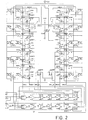
- each half section of the voltage multiplier comprises N stages: each stage is made of a capacitor and a few MOS transistors operating as switches. Said N capacitors are insulated from one another and charged in parallel to voltage Vpp during a phase of the clock signal, while, during the subsequent phase of the clock signal, said N capacitors are connected in series, to enable said capacitors, except for one of them, to be directly discharged to the output. According to the clock signal, said N capacitors are insulated from each other and are connected together by means of insulated NMOS (iso-NMOS) transistors.
- an insulated NMOS transistor is typically implemented by using a deep N-well that contains a P-well in which the NMOS transistor is realized.
- Insulated NMOS transistors are mainly built to handle negative voltages.
- the bulk of this type is insulated from the P-substrate by means of the deep N well and can be driven to different voltages, other than ground, provided that all pn junctions be never forwardly biased.
- the deep N well can be tied to the power supply voltage Vpp, whereas the P well region can be short circuited to the source region which has always to be at a voltage not higher than the drain voltage.
- said N capacitors are insulated from each other and the two terminals of each capacitor are connected one to voltage Vpp and the other one to ground GND by means of PMOS transistors.
- said N capacitors are connected in series, with the bottom plate of the first stage capacitor coupled to ground voltage GND and the top plate of the last-but-one stage capacitor coupled to the output through a PMOS transistor.
- the gate voltage of this PMOS transistor is furnished by the last stage, in the upper portion of the circuit, in order to drive the transistor into a fully on condition.
- MOS transistors only high voltage MOS transistors are employed in the circuit of Figure 2, except for the logic gates that are realized by low voltage MOS transistors.
- control signals are generated by logic gates that are shown in the bottom part of Figure 2 and effectively form a not-overlapping phase generator.
- phases PH00, PH01, PH11 and PH10 are at Vpp voltage, whereas phases PHO_N and PH1_N are at ground voltage GND.
- Capacitors C00, C01, C02, C03, C04, C10, C11, C12, C13 and C14 are charged to Vpp-Vd, where Vd is the voltage drop across the related PMOS transistor connected as a diode.
- node 18 is held at Vd by transistor NCH01 and node 12 is connected to the power supply voltage Vpp by transistor PCH01 which is on because it has the gate region coupled to ground GND and because its source region is connected to phase PH01 that is at voltage Vpp.
- each capacitor C00, C01, C02, C03, C04 and C10, C11, C12, C13, C14 is pre-charged toVpp-Vd.
- enable signal en is high and clock signal clk is in free running condition.
- clock signal clk is low
- phases PH00, PH01 and PH1_N are at voltage Vpp
- phases PHO_N, PH11 and PH10 are at ground GND.
- the left side of the voltage multiplier circuit is in charging phase, while its right side is in discharging phase.
- transistors NCH00, NCH01,NCH02 and NCH03 are off because their gate regions are at ground voltage GND and their source - drain voltages are not-negative.
- capacitors C01, C02, C03 and C04 are insulated from each other. Since phases PH00 and PH01 are at voltage Vpp and node 17 is at a proper negative voltage, as it will be evident hereinbelow, transistors PCH00, PCH01, PCH02, PCH03, PCH04, PCH05, PCH06, PCH07 and PCH08 are conductive or on, thereby fully charging capacitors C00, C01, C02, C03 and C04 to voltage Vpp.
- Transistor PCH014 that connects the upper plate of the last-but-one capacitor to the output, is off because its gate region connected to node 42 and its drain region connected to node 38 are both at ground voltage GND.
- phase PH1_N is at voltage Vpp and the voltages on node 17, on node 23, on node 24 and on node 34 are negative, transistors NCH10, NCH11, NCH12 and NCH13 are on, consequently connecting capacitors C10, C11, C12, C13 and C14 in series.
- phases PH10 and PH11 are at ground GND and node 26 is at a voltage not lower than the ground voltage GND, since the left side of the circuit is in charging phase, then transistors PCH10, PCH11, PCH12, PCH13, PCH14, PCH15, PCH16, PCH17 and PCH18 are off.
- serially connected capacitors C10, C11, C12 and C13 can be discharged to the output through transistor PCH114 which is in a fully on condition, since its gate voltage is property furnished by the last stage of the upper right portion of the circuit (capacitor C14).
- phase PH11 After the voltage of phase PH11 has gone to Vpp, the voltage of phase PH01 becomes GND, thereby discharging node 12, node 22, node 30 and node 45 through transistors PCH01, PCH03, PCH05 and PCH07 acting as diodes until they are turned off. This discharge improves the circuit performance, since parasitic capacitors are coupled to these nodes.
- a capacitor whose terminals can be driven to negative voltages is typically realized by using a layer of polysilicon, as first terminal, on an underlying thin or thick layer of gate oxide of MOS transistors, as dielectric, which is laid on a P-type diffusion region (P-well), as a second plate, which is contained in a deep N-well in order to insulate the P well from the P- substrate.
- P-well P-type diffusion region
- a P+ diffusion, in the P diffusion or P well region surrounds the polysilicon/oxide/P well vertical structure, thereby decreasing the series resistance and allowing the contacts to the P well of the second capacitor terminal to be effected.
- the pn junction which forms between the P well and the deep N well is a parasitic capacitance, associated with the capacitor, whose value is a function of the P well voltage, since the deep N well is typically connected to a fixed voltage, such as Vpp.
- This parasitic capacitance decreases as the voltage across the reverse biased pn junction increases.
- the PHO_N phase voltage subsequently takes the value Vpp, thereby turning transistors NCH00 and NCH01 on
- the PH00 phase voltage takes the GND value and transistors NCH02 and NCH03 are turned on, in view of the negative voltages applied to their source regions.
- the voltage on node 26 lowers to negative value given by V out plus the voltage across capacitor C03 minus the source-drain voltages of transistors PCH014 and NCH02.
- the negative voltage on node 26 switches transistors PCH10, PCH12, PCH14, PCH16 and PCH18 to a fully conductive state. At this time, the transitions in the circuit due to the clock signal clk are completed.
- All the high voltage MOS transistors of the circuit of Figure 2 always switch in very safe conditions so as to prevent any risk of field plate breakdown, which is a typical breakdown risk occurring in transistors switching with high voltages across them.
- several connections have been rearranged to reduce the voltage across the more stressed transistors.
- the gate regions of transistors NCH02 and NCH03, as well as the gate regions of transistors NCH12 and NCH13 are coupled to ground GND, in stead of being coupled to the PH0_N and PH1_N phase voltages.
- N tank diffusions of transistors PCH04, PCH06, PCH08, PCH011, PCH012, PCH013 and PCH014, as well as the N tank diffusions of transistors PCH14, PCH16, PCH18, PCH111, PCH112, PCH113 and PCH114 are not connected to voltage Vpp, but are properly driven by the PH01 and PH11 phase voltages, respectively.
- logic gates NAND0 and NAND1 provide the right timing to switch the voltage of the N tanks of transistors PCH07 and PCH17.
- the maximum voltage across each capacitor is only equal to the power supply voltage Vpp.
- Vpp the power supply voltage
- the capacitor dielectric is made by the MOS transistor gate oxide.
- the maximum allowed voltage across the gate oxide of a MOS transistor depends on the thickness of the gate oxide itself.
- Low voltage MOS transistors are made with a thin gate oxide which has a very high capacitance per unit area.
- high voltage MOS transistors are made with thick gate oxide, because they have to withstand high voltages; however, a thick gate oxide, compared to a thin gate oxide, has a much lower capacitance per unit area.
- the voltage multiplier according to the scheme of this invention allows a very thin gate oxide to be used for realizing the capacitors and this is a really noticeable advantage in terms of silicon area usage.
- the thin gate oxide of the MOS transistor has a thickness of 8 nm and a capacitance per unit area of about 3.8 FF/ ⁇ m 2
- the thick gate oxide of the MOS transistor has a thickness of 21 nm and a capacitance per unit area of 1.6 FF/ ⁇ m 2 .
- the silicon area needed to build the same capacitor is more than twice larger if a thick MOS gate oxide is used instead of a thin MOS gate oxide.
- the charge pump circuit of Figure 2 has been simulated by utilizing SPICE (SPICE is an acronym for Simulation Program with Integrated Circuit Emphasis) models, a clock period of 80 ns and a power supply voltage of 4 volts, furnished by a high current voltage regulator which is integrated with the embedded Flash EEPROM memory.
- SPICE Simulation Program with Integrated Circuit Emphasis
- the parasitic capacitance has been taken into account in the SPICE simulation by connecting an additional capacitor between the bottom plate of each capacitor and the power supply voltage Vpp.
- Each parasitic capacitance has been estimated at 1.2% of the capacitor value which it is associated with.
- an ideal current source I OUT has been inserted between the output and ground in order to emulate the load current.
- the waveform of the output voltage V OUT is shown in Figure 3.
- the negative voltage charge pump of Figure 2 is equivalent to an ideal voltage generator of -13.7 V serially connected to a resistor of 18 kohms.
- a voltage multiplier based upon this scheme is equivalent to an ideal voltage generator Vo with a serially connected resistor Ro the values of which, in the range of interest and with good approximation, are proportional to Vpp and to the clock period T, respectively, that is to say Vo ⁇ ⁇ * Vpp and Ro ⁇ b* T.
- the a and b coefficients depend on the circuit only. As it has been shown by the SPICE simulation, for an output current in the range 200 ⁇ A to 300 ⁇ A, the power efficiency is practically constant and equal to 33%, which is a very high value for a charge pump circuit for negative voltage.
Landscapes
- Engineering & Computer Science (AREA)
- Power Engineering (AREA)
- Dc-Dc Converters (AREA)
- Semiconductor Integrated Circuits (AREA)
- Static Random-Access Memory (AREA)
- Read Only Memory (AREA)
Applications Claiming Priority (2)
| Application Number | Priority Date | Filing Date | Title |
|---|---|---|---|
| ITRM960899 | 1996-12-23 | ||
| IT96RM000899A IT1290168B1 (it) | 1996-12-23 | 1996-12-23 | Pompa di carica a tensione negativa per memorie flash eeprom |
Publications (3)
| Publication Number | Publication Date |
|---|---|
| EP0851561A2 EP0851561A2 (en) | 1998-07-01 |
| EP0851561A3 EP0851561A3 (en) | 1999-06-30 |
| EP0851561B1 true EP0851561B1 (en) | 2002-02-27 |
Family
ID=11404615
Family Applications (1)
| Application Number | Title | Priority Date | Filing Date |
|---|---|---|---|
| EP97830710A Expired - Lifetime EP0851561B1 (en) | 1996-12-23 | 1997-12-23 | Negative voltage charge pump, particularly for flash EEPROM memories. |
Country Status (4)
| Country | Link |
|---|---|
| US (1) | US5994949A (it) |
| EP (1) | EP0851561B1 (it) |
| DE (1) | DE69710697T2 (it) |
| IT (1) | IT1290168B1 (it) |
Cited By (8)
| Publication number | Priority date | Publication date | Assignee | Title |
|---|---|---|---|---|
| US8954902B2 (en) | 2005-07-11 | 2015-02-10 | Peregrine Semiconductor Corporation | Method and apparatus improving gate oxide reliability by controlling accumulated charge |
| US9087899B2 (en) | 2005-07-11 | 2015-07-21 | Peregrine Semiconductor Corporation | Method and apparatus for use in improving linearity of MOSFETs using an accumulated charge sink-harmonic wrinkle reduction |
| US9130564B2 (en) | 2005-07-11 | 2015-09-08 | Peregrine Semiconductor Corporation | Method and apparatus for use in improving linearity of MOSFETs using an accumulated charge sink |
| US9225378B2 (en) | 2001-10-10 | 2015-12-29 | Peregrine Semiconductor Corpopration | Switch circuit and method of switching radio frequency signals |
| US9397656B2 (en) | 2005-07-11 | 2016-07-19 | Peregrine Semiconductor Corporation | Circuit and method for controlling charge injection in radio frequency switches |
| US9419565B2 (en) | 2013-03-14 | 2016-08-16 | Peregrine Semiconductor Corporation | Hot carrier injection compensation |
| US9590674B2 (en) | 2012-12-14 | 2017-03-07 | Peregrine Semiconductor Corporation | Semiconductor devices with switchable ground-body connection |
| USRE48965E1 (en) | 2005-07-11 | 2022-03-08 | Psemi Corporation | Method and apparatus improving gate oxide reliability by controlling accumulated charge |
Families Citing this family (15)
| Publication number | Priority date | Publication date | Assignee | Title |
|---|---|---|---|---|
| DE19935249C2 (de) * | 1999-07-27 | 2001-09-27 | Texas Instruments Deutschland | Gleichspannungswandler |
| JP3910765B2 (ja) * | 1999-09-08 | 2007-04-25 | 株式会社東芝 | 電圧発生回路及びこれを用いた電圧転送回路 |
| US6967523B2 (en) | 2000-11-21 | 2005-11-22 | Mosaid Technologies Incorporated | Cascaded charge pump power supply with different gate oxide thickness transistors |
| US6658629B1 (en) * | 2002-05-09 | 2003-12-02 | Sun Microsystems, Inc. | Technique for optimizing decoupling capacitance subject to leakage power constraints |
| FI114758B (fi) * | 2002-10-25 | 2004-12-15 | Nokia Oyj | Jännitekertoja |
| US7007255B2 (en) * | 2003-02-27 | 2006-02-28 | Micron Technology, Inc. | Integrated circuit design using charge pump modeling |
| US9653601B2 (en) | 2005-07-11 | 2017-05-16 | Peregrine Semiconductor Corporation | Method and apparatus for use in improving linearity of MOSFETs using an accumulated charge sink-harmonic wrinkle reduction |
| US7505298B2 (en) * | 2007-04-30 | 2009-03-17 | Spansion Llc | Transfer of non-associated information on flash memory devices |
| US8897073B2 (en) | 2012-09-14 | 2014-11-25 | Freescale Semiconductor, Inc. | NVM with charge pump and method therefor |
| US9831857B2 (en) | 2015-03-11 | 2017-11-28 | Peregrine Semiconductor Corporation | Power splitter with programmable output phase shift |
| US10505530B2 (en) | 2018-03-28 | 2019-12-10 | Psemi Corporation | Positive logic switch with selectable DC blocking circuit |
| US10236872B1 (en) | 2018-03-28 | 2019-03-19 | Psemi Corporation | AC coupling modules for bias ladders |
| US10886911B2 (en) | 2018-03-28 | 2021-01-05 | Psemi Corporation | Stacked FET switch bias ladders |
| US11476849B2 (en) | 2020-01-06 | 2022-10-18 | Psemi Corporation | High power positive logic switch |
| US11502619B1 (en) * | 2021-07-30 | 2022-11-15 | Texas Instruments Incorporated | Hybrid multi-level inverter and charge pump |
Family Cites Families (8)
| Publication number | Priority date | Publication date | Assignee | Title |
|---|---|---|---|---|
| US5168174A (en) * | 1991-07-12 | 1992-12-01 | Texas Instruments Incorporated | Negative-voltage charge pump with feedback control |
| US5301097A (en) * | 1992-06-10 | 1994-04-05 | Intel Corporation | Multi-staged charge-pump with staggered clock phases for providing high current capability |
| JPH0828965B2 (ja) * | 1992-09-02 | 1996-03-21 | 日本電気株式会社 | 電圧変換回路 |
| US5414614A (en) * | 1994-06-06 | 1995-05-09 | Motorola, Inc. | Dynamically configurable switched capacitor power supply and method |
| IT1275104B (it) * | 1994-12-28 | 1997-07-30 | Texas Instruments Italia Spa | "perfezionato moltiplicatore di tensione on-chip per memorie a semiconduttore" |
| KR0179852B1 (ko) * | 1995-10-25 | 1999-04-15 | 문정환 | 차지 펌프 회로 |
| EP0772282B1 (en) * | 1995-10-31 | 2000-03-15 | STMicroelectronics S.r.l. | Negative charge pump circuit for electrically erasable semiconductor memory devices |
| US5856918A (en) * | 1995-11-08 | 1999-01-05 | Sony Corporation | Internal power supply circuit |
-
1996
- 1996-12-23 IT IT96RM000899A patent/IT1290168B1/it active IP Right Grant
-
1997
- 1997-12-19 US US08/994,470 patent/US5994949A/en not_active Expired - Lifetime
- 1997-12-23 DE DE69710697T patent/DE69710697T2/de not_active Expired - Lifetime
- 1997-12-23 EP EP97830710A patent/EP0851561B1/en not_active Expired - Lifetime
Cited By (8)
| Publication number | Priority date | Publication date | Assignee | Title |
|---|---|---|---|---|
| US9225378B2 (en) | 2001-10-10 | 2015-12-29 | Peregrine Semiconductor Corpopration | Switch circuit and method of switching radio frequency signals |
| US8954902B2 (en) | 2005-07-11 | 2015-02-10 | Peregrine Semiconductor Corporation | Method and apparatus improving gate oxide reliability by controlling accumulated charge |
| US9087899B2 (en) | 2005-07-11 | 2015-07-21 | Peregrine Semiconductor Corporation | Method and apparatus for use in improving linearity of MOSFETs using an accumulated charge sink-harmonic wrinkle reduction |
| US9130564B2 (en) | 2005-07-11 | 2015-09-08 | Peregrine Semiconductor Corporation | Method and apparatus for use in improving linearity of MOSFETs using an accumulated charge sink |
| US9397656B2 (en) | 2005-07-11 | 2016-07-19 | Peregrine Semiconductor Corporation | Circuit and method for controlling charge injection in radio frequency switches |
| USRE48965E1 (en) | 2005-07-11 | 2022-03-08 | Psemi Corporation | Method and apparatus improving gate oxide reliability by controlling accumulated charge |
| US9590674B2 (en) | 2012-12-14 | 2017-03-07 | Peregrine Semiconductor Corporation | Semiconductor devices with switchable ground-body connection |
| US9419565B2 (en) | 2013-03-14 | 2016-08-16 | Peregrine Semiconductor Corporation | Hot carrier injection compensation |
Also Published As
| Publication number | Publication date |
|---|---|
| US5994949A (en) | 1999-11-30 |
| DE69710697D1 (de) | 2002-04-04 |
| IT1290168B1 (it) | 1998-10-19 |
| EP0851561A3 (en) | 1999-06-30 |
| EP0851561A2 (en) | 1998-07-01 |
| DE69710697T2 (de) | 2002-09-05 |
| ITRM960899A1 (it) | 1998-06-23 |
| ITRM960899A0 (it) | 1996-12-23 |
Similar Documents
| Publication | Publication Date | Title |
|---|---|---|
| EP0851561B1 (en) | Negative voltage charge pump, particularly for flash EEPROM memories. | |
| US6023188A (en) | Positive/negative high voltage charge pump system | |
| US6130572A (en) | NMOS negative charge pump | |
| US7135911B2 (en) | Potential detector and semiconductor integrated circuit | |
| KR101039236B1 (ko) | 면적 효율성을 고려한 충전 펌프 및 전압 생성 방법 | |
| US6878981B2 (en) | Triple-well charge pump stage with no threshold voltage back-bias effect | |
| US6501325B1 (en) | Low voltage supply higher efficiency cross-coupled high voltage charge pumps | |
| US6914791B1 (en) | High efficiency triple well charge pump circuit | |
| USRE41217E1 (en) | Method and apparatus for reducing stress across capacitors used in integrated circuits | |
| US5892267A (en) | Multi-stage voltage-boosting circuit with boosted back-gate bias | |
| EP1899785B1 (en) | Efficient charge pump for a wide range of supply voltages | |
| US6418040B1 (en) | Bi-directional architecture for a high-voltage cross-coupled charge pump | |
| US20050248386A1 (en) | Four phase charge pump operable without phase overlap with improved efficiency | |
| US6356137B1 (en) | Voltage boost circuit with low power supply voltage | |
| JP5537307B2 (ja) | チャージポンプ回路、不揮発性メモリ、データ処理装置、及びマイクロコンピュータ応用システム | |
| EP0865149B1 (en) | High current CMOS charge pump, particularly for flash EEPROM memories | |
| US5543668A (en) | Charge stacking on-chip high-voltage generator and method | |
| Tanzawa | Innovation of switched-capacitor voltage multiplier: Part 3: State of the art of switching circuits and applications of charge pumps | |
| Khouri et al. | Improved charge pump for flash memory applications in triple well CMOS technology | |
| US6285243B1 (en) | High-voltage charge pump circuit | |
| EP0851562B1 (en) | High voltage charge pump, particularly for flash EEPROM memories | |
| WO1998016010A1 (en) | Triple well charge pump | |
| US7148739B2 (en) | Charge pump element with body effect cancellation for early charge pump stages | |
| WO1998028673A1 (en) | Precise medium voltage, high current charge pump system |
Legal Events
| Date | Code | Title | Description |
|---|---|---|---|
| PUAI | Public reference made under article 153(3) epc to a published international application that has entered the european phase |
Free format text: ORIGINAL CODE: 0009012 |
|
| AK | Designated contracting states |
Kind code of ref document: A2 Designated state(s): DE FR GB IT NL |
|
| AX | Request for extension of the european patent |
Free format text: AL;LT;LV;MK;RO;SI |
|
| PUAL | Search report despatched |
Free format text: ORIGINAL CODE: 0009013 |
|
| AK | Designated contracting states |
Kind code of ref document: A3 Designated state(s): AT BE CH DE DK ES FI FR GB GR IE IT LI LU MC NL PT SE |
|
| AX | Request for extension of the european patent |
Free format text: AL;LT;LV;MK;RO;SI |
|
| 17P | Request for examination filed |
Effective date: 19991116 |
|
| AKX | Designation fees paid |
Free format text: DE FR GB IT NL |
|
| 17Q | First examination report despatched |
Effective date: 20000726 |
|
| RAP1 | Party data changed (applicant data changed or rights of an application transferred) |
Owner name: CONSORZIO EAGLE Owner name: TEXAS INSTRUMENTS INCORPORATED |
|
| GRAG | Despatch of communication of intention to grant |
Free format text: ORIGINAL CODE: EPIDOS AGRA |
|
| GRAG | Despatch of communication of intention to grant |
Free format text: ORIGINAL CODE: EPIDOS AGRA |
|
| GRAH | Despatch of communication of intention to grant a patent |
Free format text: ORIGINAL CODE: EPIDOS IGRA |
|
| GRAH | Despatch of communication of intention to grant a patent |
Free format text: ORIGINAL CODE: EPIDOS IGRA |
|
| GRAH | Despatch of communication of intention to grant a patent |
Free format text: ORIGINAL CODE: EPIDOS IGRA |
|
| REG | Reference to a national code |
Ref country code: GB Ref legal event code: IF02 |
|
| GRAA | (expected) grant |
Free format text: ORIGINAL CODE: 0009210 |
|
| AK | Designated contracting states |
Kind code of ref document: B1 Designated state(s): DE FR GB IT NL |
|
| REF | Corresponds to: |
Ref document number: 69710697 Country of ref document: DE Date of ref document: 20020404 |
|
| ET | Fr: translation filed | ||
| PLBE | No opposition filed within time limit |
Free format text: ORIGINAL CODE: 0009261 |
|
| STAA | Information on the status of an ep patent application or granted ep patent |
Free format text: STATUS: NO OPPOSITION FILED WITHIN TIME LIMIT |
|
| 26N | No opposition filed |
Effective date: 20021128 |
|
| PGFP | Annual fee paid to national office [announced via postgrant information from national office to epo] |
Ref country code: GB Payment date: 20121128 Year of fee payment: 16 Ref country code: IT Payment date: 20121220 Year of fee payment: 16 |
|
| PGFP | Annual fee paid to national office [announced via postgrant information from national office to epo] |
Ref country code: NL Payment date: 20121212 Year of fee payment: 16 Ref country code: FR Payment date: 20121219 Year of fee payment: 16 |
|
| PGFP | Annual fee paid to national office [announced via postgrant information from national office to epo] |
Ref country code: DE Payment date: 20121221 Year of fee payment: 16 |
|
| REG | Reference to a national code |
Ref country code: DE Ref legal event code: R119 Ref document number: 69710697 Country of ref document: DE |
|
| REG | Reference to a national code |
Ref country code: NL Ref legal event code: V1 Effective date: 20140701 |
|
| GBPC | Gb: european patent ceased through non-payment of renewal fee |
Effective date: 20131223 |
|
| REG | Reference to a national code |
Ref country code: DE Ref legal event code: R119 Ref document number: 69710697 Country of ref document: DE Effective date: 20140701 |
|
| REG | Reference to a national code |
Ref country code: FR Ref legal event code: ST Effective date: 20140829 |
|
| PG25 | Lapsed in a contracting state [announced via postgrant information from national office to epo] |
Ref country code: DE Free format text: LAPSE BECAUSE OF NON-PAYMENT OF DUE FEES Effective date: 20140701 Ref country code: NL Free format text: LAPSE BECAUSE OF NON-PAYMENT OF DUE FEES Effective date: 20140701 |
|
| PG25 | Lapsed in a contracting state [announced via postgrant information from national office to epo] |
Ref country code: FR Free format text: LAPSE BECAUSE OF NON-PAYMENT OF DUE FEES Effective date: 20131231 Ref country code: GB Free format text: LAPSE BECAUSE OF NON-PAYMENT OF DUE FEES Effective date: 20131223 |
|
| PG25 | Lapsed in a contracting state [announced via postgrant information from national office to epo] |
Ref country code: IT Free format text: LAPSE BECAUSE OF NON-PAYMENT OF DUE FEES Effective date: 20131231 |
|
| PG25 | Lapsed in a contracting state [announced via postgrant information from national office to epo] |
Ref country code: IT Free format text: LAPSE BECAUSE OF NON-PAYMENT OF DUE FEES Effective date: 20131223 |