EP0853280A2 - Procédé et appareil de verification temporelle - Google Patents
Procédé et appareil de verification temporelle Download PDFInfo
- Publication number
- EP0853280A2 EP0853280A2 EP98100318A EP98100318A EP0853280A2 EP 0853280 A2 EP0853280 A2 EP 0853280A2 EP 98100318 A EP98100318 A EP 98100318A EP 98100318 A EP98100318 A EP 98100318A EP 0853280 A2 EP0853280 A2 EP 0853280A2
- Authority
- EP
- European Patent Office
- Prior art keywords
- circuit
- timing verification
- circuit portion
- timing
- asynchronous
- Prior art date
- Legal status (The legal status is an assumption and is not a legal conclusion. Google has not performed a legal analysis and makes no representation as to the accuracy of the status listed.)
- Withdrawn
Links
Images


Classifications
-
- G—PHYSICS
- G06—COMPUTING OR CALCULATING; COUNTING
- G06F—ELECTRIC DIGITAL DATA PROCESSING
- G06F30/00—Computer-aided design [CAD]
- G06F30/30—Circuit design
- G06F30/32—Circuit design at the digital level
- G06F30/33—Design verification, e.g. functional simulation or model checking
- G06F30/3308—Design verification, e.g. functional simulation or model checking using simulation
- G06F30/3312—Timing analysis
Definitions
- the present invention relates to a timing verification method and device which verify a design of an electric or electronic circuit.
- an electric circuit or an electronic circuit constituted of IC and LSI operates at a timing as designed.
- the circuit available are a synchronous circuit in which a flip-flop, a latch circuit or another circuit element operates with one clock and an asynchronous circuit in which the circuit element operates with plural clocks.
- a static verification device is used for verifying a setup time or a hold time from one latch circuit to another latch circuit, while to verify timings of synchronous and asynchronous circuits a dynamic verification device is used for preparing a test pattern to perform a simulation.
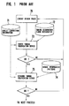
- Fig. 1 is an explanatory view of a process flow in a conventional timing verification method for an electric or electronic circuit.
- reference numeral 71 denotes a circuit connection information to be verified
- 72 a timing designation and clock designation information of an input/output signal
- 73 a conventional static timing verification device
- 74 a signal information (pattern)
- 75 a dynamic timing verification device
- 76 a circuit design phase.
- the conventional static timing verification device 73 basically requires no signal information of each circuit element by means of simulation.
- timing and clock of the input/output signal (refer to 72 in Fig. 1)
- a latest path (critical path) between latches is found to verify the setup timing by determining whether or not the critical path is in time as compared with a clock cycle.
- a fastest path between the latches is found to verify the hold timing by determining whether or not the next data is taken in at the timing of the same clock.
- the dynamic timing verification device 75 shown in Fig. 1 requires the signal information (test pattern) 74 of each circuit element by means of simulation. By transmitting the signal information 74 into an input terminal of the circuit connection information 71, the circuit connection of the verified circuit is activated and simulation is performed.
- a predetermined clock cycle it is determined by tracing a state of an output terminal of the circuit connection information 71 whether or not the circuit connection of the verified circuit is operated as expected.
- the setup timing, the hold timing, a spike timing or another timing is verified.
- a publication of patent application laid-open No. Hei 4-288677 proposes a constitution of a timing verification device for a synchronous/asynchronous mixed type of circuit to be verified in which synchronous/asynchronous circuit portions are automatically identified. By dividing the circuit to be verified into respective circuit portions, the timing of each circuit portion can be appropriately verified, so that all the timing problems can be found in a short time. In the device, first only the synchronous circuit portion which requires no test pattern is checked, and for the remaining circuit portion the timing verification for which the test pattern is necessary is performed.
- a problem with the conventional timing verification operation lies in that the conventional static verification device only verifies the timing of the synchronous circuit with a designated clock. Therefore, the timing of the asynchronous circuit portion has to be verified by using a separate dynamic timing verification device.
- the signal information with which a malfunction of the asynchronous portion can be detected is necessary. Disadvantages are that preparation of the information takes time and much simulation time is required. Further, only when tracing an output of the circuit connection information to determine whether or not the output data is a desired data, it is known whether or not the timing of an internal circuit is satisfactory. Therefore, if output information provides no expected value, it disadvantageously takes much time to analyze in which connection portion of the circuit connection information a timing violation occurs.
- the reason for the above is that since the conventional static timing verification device can easily verify the timing of the synchronous circuit portion, but hardly verify the timing of the asynchronous circuit portion, the timing verification of the asynchronous circuit portion is performed only by the dynamic timing verification device.
- a static timing verification device extracts the delay of the designated paths and verifies based on the delay data whether or not a designated delay relationship is established, to verify the timing of the circuit.
- an object of the invention is to provide a timing verification device for a synchronous/asynchronous mixed circuit which can verify timings of a synchronous circuit portion and an asynchronous circuit portion by means of a static timing verification.
- Another object of the invention is to provide a timing verification device which can largely reduce a time necessary for timing verification.
- the invention provides a timing verification method for a synchronous circuit/asynchronous circuit mixed circuit in which paths are designated in a circuit portion in which a delay becomes a problem associated with an asynchronous circuit portion, a delay information of the paths is obtained, and it is verified whether or not the delay information satisfies a designated delay relationship among the paths in the circuit portion.
- the timing of the asynchronous circuit portion can be verified only by means of a static timing verification without using a test pattern.
- the present invention provides a timing verification device for verifying a timing of a synchronous circuit/asynchronous circuit mixed circuit which is provided with a means for storing designated paths in a circuit portion having a problem of delay associated with an asynchronous circuit portion and a path relationship information and a means for verifying from obtained delay values of the designated paths whether or not the delay values of the paths satisfy a designated delay condition of the paths. Timings of not only the synchronous circuit but also the asynchronous circuit portion are verified only by means of a static timing verification without using a test pattern.
- Fig. 1 is a flowchart showing a process in a prior-art timing verification system.
- Fig. 2 is a flowchart of a timing verification process in an embodiment according to the invention.
- Fig. 3 is a flowchart of a process in a static timing verification device according to an embodiment of the invention.
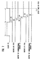
- Fig. 4 is a circuit diagram showing a constitution of a sample circuit to depict a static timing verification method of an asynchronous circuit portion in an embodiment of the invention.
- Fig. 5 is a timing chart of an operation in the sample circuit in Fig. 4.
- Fig. 7 is a timing chart of an operation in the sample circuit in Fig. 6.
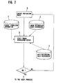
- Fig. 2 is an explanatory view of a process flow in a timing verification method according to an embodiment of the invention.
- reference numeral 1 denotes a circuit connection information to be verified
- 2 a timing designation and clock designation information of an input/output signal
- 7 an information for designating paths to be measured in an asynchronous circuit portion and designating a relationship between the paths
- 5 a static timing verification device
- 6 a circuit preparation phase.
- the flow of process in the timing verification according to the embodiment differs from the conventional flow of process shown in Fig. 1 in that no dynamic timing verification device for an asynchronous circuit portion is provided. Specifically, in the embodiment of the invention, since the timing verification of the asynchronous circuit portion is performed by the static timing verification device, no dynamic timing verification device for the asynchronous circuit portion is required.
- the static timing verification device basically without using the signal information of each circuit element by means of simulation, by designating timing and clock of an input/output signal (refer to the timing designation and clock designation information 2), a latest path (critical path) is found between latches in a circuit portion which is synchronous with a clock designated signal to verify a setup timing by determining whether or not the path is in time as compared with a clock cycle. Also, a fastest path between the latches is found to verify a hold timing by determining whether or not the next data is taken in at the timing of the same clock.
- the verification means takes the same method as the prior-art static timing verification tool shown in Fig. 1.
- a delay information in the paths designated in the measured path designation and path relationship designation information 7 is extracted.
- the path delay data which is already extracted in the static timing verification phase 8 for the synchronous circuit portion can be used.
- the extracted value (the delay value of the designated path)
- the timing of the asynchronous circuit portion is verified.
- Fig. 4 is an explanatory view of a first embodiment according to the invention, showing a constitution of a sample circuit to depict the static timing verification method for the asynchronous circuit portion.
- reference numeral 10 denotes a fall synchronous flip-flop (hereinafter, referred to as FF), 11 a two-input AND circuit, 12 a buffer circuit, 13 an enable signal, 14 a clock A system clock, and 15 a clock B system clock.
- FF fall synchronous flip-flop
- the enable signal 13 is connected to a data input terminal D of the FF10
- the clock A system clock 14 is connected to a clock input terminal C of the FF10 and to an input terminal of the buffer circuit 12
- an output terminal Q of the FF10 is connected to an input terminal A of the AND circuit 11
- an output terminal of the buffer circuit 12 is connected to the other input terminal B of the AND circuit 11, and an output terminal of the AND circuit 11 emits the clock B system clock 15.
- the clock B system clock 15 is prepared from the clock A system clock 14, and supplied as an active clock only when the enable signal 13 is logically "1".
- a broken line 16 denotes a path delay of [the output of the clock A system clock 14]-[the clock input C of the FF10]-[the output Q of the FF10]-[the input A of the AND circuit 11].
Landscapes
- Engineering & Computer Science (AREA)
- Computer Hardware Design (AREA)
- Physics & Mathematics (AREA)
- Theoretical Computer Science (AREA)
- Evolutionary Computation (AREA)
- Geometry (AREA)
- General Engineering & Computer Science (AREA)
- General Physics & Mathematics (AREA)
- Tests Of Electronic Circuits (AREA)
Applications Claiming Priority (2)
| Application Number | Priority Date | Filing Date | Title |
|---|---|---|---|
| JP9014554A JP3036454B2 (ja) | 1997-01-10 | 1997-01-10 | タイミング検証方法及び装置 |
| JP14554/97 | 1997-01-10 |
Publications (2)
| Publication Number | Publication Date |
|---|---|
| EP0853280A2 true EP0853280A2 (fr) | 1998-07-15 |
| EP0853280A3 EP0853280A3 (fr) | 1998-07-22 |
Family
ID=11864377
Family Applications (1)
| Application Number | Title | Priority Date | Filing Date |
|---|---|---|---|
| EP98100318A Withdrawn EP0853280A3 (fr) | 1997-01-10 | 1998-01-09 | Procédé et appareil de verification temporelle |
Country Status (2)
| Country | Link |
|---|---|
| EP (1) | EP0853280A3 (fr) |
| JP (1) | JP3036454B2 (fr) |
Cited By (1)
| Publication number | Priority date | Publication date | Assignee | Title |
|---|---|---|---|---|
| WO1999063664A3 (fr) * | 1998-05-29 | 2002-10-03 | Siemens Ag | Dispositif et procede pour synchroniser un signal asynchrone en synthese et simuler un circuit cadence |
Families Citing this family (1)
| Publication number | Priority date | Publication date | Assignee | Title |
|---|---|---|---|---|
| JP2005172549A (ja) | 2003-12-10 | 2005-06-30 | Matsushita Electric Ind Co Ltd | 半導体集積回路の検証方法及びテストパターンの作成方法 |
Family Cites Families (1)
| Publication number | Priority date | Publication date | Assignee | Title |
|---|---|---|---|---|
| US5572717A (en) * | 1994-04-06 | 1996-11-05 | Altera Corporation | Method and apparatus for assigning and analyzing timing specifications in a computer aided engineering program |
-
1997
- 1997-01-10 JP JP9014554A patent/JP3036454B2/ja not_active Expired - Lifetime
-
1998
- 1998-01-09 EP EP98100318A patent/EP0853280A3/fr not_active Withdrawn
Cited By (2)
| Publication number | Priority date | Publication date | Assignee | Title |
|---|---|---|---|---|
| WO1999063664A3 (fr) * | 1998-05-29 | 2002-10-03 | Siemens Ag | Dispositif et procede pour synchroniser un signal asynchrone en synthese et simuler un circuit cadence |
| US7072821B1 (en) | 1998-05-29 | 2006-07-04 | Siemens Aktiengesellschaft | Device and method for synchronizing an asynchronous signal in synthesis and simulation of a clocked circuit |
Also Published As
| Publication number | Publication date |
|---|---|
| EP0853280A3 (fr) | 1998-07-22 |
| JP3036454B2 (ja) | 2000-04-24 |
| JPH10198723A (ja) | 1998-07-31 |
Similar Documents
| Publication | Publication Date | Title |
|---|---|---|
| US5579510A (en) | Method and structure for use in static timing verification of synchronous circuits | |
| KR19980032933A (ko) | 에뮬레이션 및 시뮬레이션을 이용한 설계 검증 방법 및 장치 | |
| US8738352B2 (en) | Managing communication bandwidth in co-verification of circuit designs | |
| US5771375A (en) | Automatic delay adjustment for static timing analysis using clock edge identification and half cycle paths | |
| US6698005B2 (en) | Min-time / race margins in digital circuits | |
| US9954534B2 (en) | Methods and circuits for preventing hold time violations | |
| EP0280848A2 (fr) | Système sur puce de détection en ligne d'erreur en courant alternatif et en courant continu d'arbre d'horloge | |
| US6871329B2 (en) | Design system of integrated circuit and its design method and program | |
| EP0853280A2 (fr) | Procédé et appareil de verification temporelle | |
| US6546531B1 (en) | Automatic delay element insertion system for addressing holdtime problems | |
| JP2778443B2 (ja) | スキャンパステスト回路の最適化方法 | |
| US6246971B1 (en) | Testing asynchronous circuits | |
| JP5145167B2 (ja) | クロックドメインチェック方法及びクロックドメインチェック用プログラム並びに記録媒体 | |
| US6973422B1 (en) | Method and apparatus for modeling and circuits with asynchronous behavior | |
| US6067647A (en) | Method and apparatus for inserting an error signal onto a bidirectional signal line | |
| JPH05189517A (ja) | シミュレーション回路 | |
| US7072821B1 (en) | Device and method for synchronizing an asynchronous signal in synthesis and simulation of a clocked circuit | |
| US10230374B1 (en) | Methods and circuits for preventing hold violations | |
| US6111898A (en) | Method of establishing when to propagate the output of a multiplexer | |
| JP2962232B2 (ja) | スキャンパス回路の自動配置配線方法 | |
| JP2914257B2 (ja) | 競合動作の判定方法 | |
| JP2984522B2 (ja) | 回路検証システム | |
| JPH04357569A (ja) | 論理シミュレータ | |
| JP3123982B2 (ja) | 論理シミュレーション方法 | |
| JPH117461A (ja) | 論理シミュレーション方法およびテストパターン生成装置 |
Legal Events
| Date | Code | Title | Description |
|---|---|---|---|
| PUAI | Public reference made under article 153(3) epc to a published international application that has entered the european phase |
Free format text: ORIGINAL CODE: 0009012 |
|
| PUAL | Search report despatched |
Free format text: ORIGINAL CODE: 0009013 |
|
| AK | Designated contracting states |
Kind code of ref document: A2 Designated state(s): DE FR GB |
|
| AX | Request for extension of the european patent |
Free format text: AL;LT;LV;MK;RO;SI |
|
| AK | Designated contracting states |
Kind code of ref document: A3 Designated state(s): AT BE CH DE DK ES FI FR GB GR IE IT LI LU MC NL PT SE |
|
| AX | Request for extension of the european patent |
Free format text: AL;LT;LV;MK;RO;SI |
|
| 17P | Request for examination filed |
Effective date: 19980618 |
|
| AKX | Designation fees paid |
Free format text: DE FR GB |
|
| RBV | Designated contracting states (corrected) |
Designated state(s): DE FR GB |
|
| 17Q | First examination report despatched |
Effective date: 20020314 |
|
| STAA | Information on the status of an ep patent application or granted ep patent |
Free format text: STATUS: THE APPLICATION IS DEEMED TO BE WITHDRAWN |
|
| 18D | Application deemed to be withdrawn |
Effective date: 20020725 |