EP0853386A2 - Frequenzregelungsanordnung - Google Patents
Frequenzregelungsanordnung Download PDFInfo
- Publication number
- EP0853386A2 EP0853386A2 EP97310534A EP97310534A EP0853386A2 EP 0853386 A2 EP0853386 A2 EP 0853386A2 EP 97310534 A EP97310534 A EP 97310534A EP 97310534 A EP97310534 A EP 97310534A EP 0853386 A2 EP0853386 A2 EP 0853386A2
- Authority
- EP
- European Patent Office
- Prior art keywords
- frequency
- oscillator
- clock
- mark
- control arrangement
- Prior art date
- Legal status (The legal status is an assumption and is not a legal conclusion. Google has not performed a legal analysis and makes no representation as to the accuracy of the status listed.)
- Withdrawn
Links
Images

Classifications
-
- H—ELECTRICITY
- H03—ELECTRONIC CIRCUITRY
- H03J—TUNING RESONANT CIRCUITS; SELECTING RESONANT CIRCUITS
- H03J7/00—Automatic frequency control; Automatic scanning over a band of frequencies
- H03J7/02—Automatic frequency control
-
- G—PHYSICS
- G11—INFORMATION STORAGE
- G11B—INFORMATION STORAGE BASED ON RELATIVE MOVEMENT BETWEEN RECORD CARRIER AND TRANSDUCER
- G11B20/00—Signal processing not specific to the method of recording or reproducing; Circuits therefor
- G11B20/10—Digital recording or reproducing
- G11B20/14—Digital recording or reproducing using self-clocking codes
- G11B20/1403—Digital recording or reproducing using self-clocking codes characterised by the use of two levels
- G11B20/1423—Code representation depending on subsequent bits, e.g. delay modulation, double density code, Miller code
- G11B20/1426—Code representation depending on subsequent bits, e.g. delay modulation, double density code, Miller code conversion to or from block codes or representations thereof
-
- H—ELECTRICITY
- H03—ELECTRONIC CIRCUITRY
- H03J—TUNING RESONANT CIRCUITS; SELECTING RESONANT CIRCUITS
- H03J7/00—Automatic frequency control; Automatic scanning over a band of frequencies
- H03J7/18—Automatic scanning over a band of frequencies
-
- H—ELECTRICITY
- H03—ELECTRONIC CIRCUITRY
- H03L—AUTOMATIC CONTROL, STARTING, SYNCHRONISATION OR STABILISATION OF GENERATORS OF ELECTRONIC OSCILLATIONS OR PULSES
- H03L7/00—Automatic control of frequency or phase; Synchronisation
- H03L7/06—Automatic control of frequency or phase; Synchronisation using a reference signal applied to a frequency- or phase-locked loop
- H03L7/08—Details of the phase-locked loop
- H03L7/085—Details of the phase-locked loop concerning mainly the frequency- or phase-detection arrangement including the filtering or amplification of its output signal
- H03L7/087—Details of the phase-locked loop concerning mainly the frequency- or phase-detection arrangement including the filtering or amplification of its output signal using at least two phase detectors or a frequency and phase detector in the loop
-
- H—ELECTRICITY
- H03—ELECTRONIC CIRCUITRY
- H03L—AUTOMATIC CONTROL, STARTING, SYNCHRONISATION OR STABILISATION OF GENERATORS OF ELECTRONIC OSCILLATIONS OR PULSES
- H03L7/00—Automatic control of frequency or phase; Synchronisation
- H03L7/06—Automatic control of frequency or phase; Synchronisation using a reference signal applied to a frequency- or phase-locked loop
- H03L7/08—Details of the phase-locked loop
- H03L7/099—Details of the phase-locked loop concerning mainly the controlled oscillator of the loop
- H03L7/0995—Details of the phase-locked loop concerning mainly the controlled oscillator of the loop the oscillator comprising a ring oscillator
-
- H—ELECTRICITY
- H03—ELECTRONIC CIRCUITRY
- H03L—AUTOMATIC CONTROL, STARTING, SYNCHRONISATION OR STABILISATION OF GENERATORS OF ELECTRONIC OSCILLATIONS OR PULSES
- H03L7/00—Automatic control of frequency or phase; Synchronisation
- H03L7/06—Automatic control of frequency or phase; Synchronisation using a reference signal applied to a frequency- or phase-locked loop
- H03L7/08—Details of the phase-locked loop
- H03L7/10—Details of the phase-locked loop for assuring initial synchronisation or for broadening the capture range
- H03L7/113—Details of the phase-locked loop for assuring initial synchronisation or for broadening the capture range using frequency discriminator
-
- H—ELECTRICITY
- H03—ELECTRONIC CIRCUITRY
- H03L—AUTOMATIC CONTROL, STARTING, SYNCHRONISATION OR STABILISATION OF GENERATORS OF ELECTRONIC OSCILLATIONS OR PULSES
- H03L7/00—Automatic control of frequency or phase; Synchronisation
- H03L7/06—Automatic control of frequency or phase; Synchronisation using a reference signal applied to a frequency- or phase-locked loop
- H03L7/16—Indirect frequency synthesis, i.e. generating a desired one of a number of predetermined frequencies using a frequency- or phase-locked loop
- H03L7/18—Indirect frequency synthesis, i.e. generating a desired one of a number of predetermined frequencies using a frequency- or phase-locked loop using a frequency divider or counter in the loop
-
- G—PHYSICS
- G11—INFORMATION STORAGE
- G11B—INFORMATION STORAGE BASED ON RELATIVE MOVEMENT BETWEEN RECORD CARRIER AND TRANSDUCER
- G11B20/00—Signal processing not specific to the method of recording or reproducing; Circuits therefor
- G11B20/10—Digital recording or reproducing
- G11B20/14—Digital recording or reproducing using self-clocking codes
- G11B20/1403—Digital recording or reproducing using self-clocking codes characterised by the use of two levels
- G11B20/1423—Code representation depending on subsequent bits, e.g. delay modulation, double density code, Miller code
- G11B20/1426—Code representation depending on subsequent bits, e.g. delay modulation, double density code, Miller code conversion to or from block codes or representations thereof
- G11B2020/1461—8 to 14 modulation, e.g. the EFM code used on CDs or mini-discs
Definitions
- the present invention relates to a frequency control arrangement and more particularly, though not exclusively, to a frequency control arrangement suitable for use in a wideband phase locked loop.
- Wideband phase locked loops are widely used in the extraction of data from CD-ROMs and digital video data (DVD) ROMs. They are essentially used to generate a clock signal which is synchronous with an incoming efm data signal and to output the clock signal with the efm data signal.
- Efm data is required to contain a maximum mark or space at least once in a specified number of data intervals.
- the efm data is required to contain a maximum mark or space of 11T every 588 written T intervals.
- DVD-ROM efm data is required to contain a maximum mark or space of 14T every 1488 written T intervals. This requirement of the efm data allows detector circuitry to be synchronised to the efm data stream by allowing the frequency of the efm data stream to be detected.
- This frequency detection is performs digitally by measuring the maximum mark or space but the resolution of the measurement is limited by the clock frequency of the frequency detector circuit. It is not generally possible to increase the clock frequency because the clock signal is output to data recovery circuitry as being synchronous with the incoming efm data stream.
- a frequency control arrangement comprising an oscillator, a mark or space counter, a frequency detector and an error signal calculator in which it is desired to control the oscillator to resonate at a frequency substantially equal to the frequency of a received data stream, the oscillator being a ring oscillator which is arranged to provide phased clock signals on respective output lines to the mark or space counter thereby to allow the mark or space counter to measure the length of the marks or spaces of the data with increased resolution.
- a frequency control arrangement for controlling an oscillator to operate at a frequency substantially equal to the clock frequency of a received stream of data signals, wherein the oscillator is a ring oscillator which is arranged to provide a plurality of clock signals of different phases on respective output lines to a mark or space counter to clock into said counter the instantaneous value of said data signals at a like plurality of intervals within a cycle of said clock frequency.
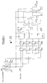
- mark or space counter 100 comprises ring oscillator 110 and logic circuit 120.
- Ring oscillator 110 comprises controllable delay elements 111 and 112 and invertors 113 and 114.
- the output electrode of delay element 111 is connected to a first clock line and to the input electrode of delay element 112.
- the output electrode of delay element 112 is connected to a second clock line and to the input electrode of invertor 113, the output electrode of which is connected to a fourth clock line.
- Inventor 114 has its input electrode connected to the output of delay element 111 and its output electrode connected to a third clock line.
- the output of delay element 112 is connected to the inverting input electrode of delay element 111.
- Delay elements 111 and 112 are each controlled by a signal on frequency control line 190.
- Ring oscillator 110 operates to output four-phase clock pulses on the first to fourth clock lines at a frequency dependent on current signal received on frequency control line 190.
- a ring oscillator which could be used as ring oscillator 110 is described in United States Patent No. US 5304938.
- D-type flip-flops 121-124 are clocked by the first to fourth clock lines respectively and each have their input connected to data input line 170 to receive incoming efm data.
- D-types 125-128 have their inputs connected to the respective outputs of D-types 121-124.
- D-types 125 - 128 are each clocked by the first clock line and have their outputs connected to first to fourth inputs of logic calculator 130 respectively.
- Logic calculator 130 has three outputs, a "transition” output, a "remainder” output and an "add" output. The transition output is connected to the input of D-type 129, the remainder output is connected to the input of latch 140 and the add output is connected to a first input of adder 160.
- the output of D-type 129 is connected to the enable input of latch 142 and to the control input of mux 150.
- the output of latch 140 is connected to a first signal input of mux 150, the output of which is connected to the second input of adder 160.
- the output of adder 160 is connected to the input of latch 141.
- the output of latch 141 is connected to both the input of latch 142 and the second signal input of mux 150.
- D-type 129, latches 140 - 142, logic calculator 130 and mux 150 are all clocked by the first clock line.
- the output of latch 142 is connected to result line 180.
- D-types 121 - 129 each operate to hold as their output, the logic level that is present on their input at the rising clock edge.
- D-types 121 - 124 thus present at their respective outputs the data signal present on data input line 170 at four-phase intervals of the clock period.
- These data signals are clocked at the phase of the first clock by D-types 125-128. This ensures that each of the logic calculator inputs receives different ones of the four-phase clocked data input signal.
- Logic calculator 130 comprises a single memory element, which stores the logic value of D-type 128 from the previous cycle, and combinational logic to produce certain output signals, which will now be described.
- the transition output will be high.
- the add output will be equal to the number of inputs which have the same logic level as that stored in the memory element and the remainder output will be equal to four minus the value of the add output. In all other instances the transition output will be low, the add output will be four and the remainder output will be zero.
- the number of successive quadrature clocks on which the same logic level was input on data input line 170 can then be calculated in adder 160 by virtue of latches 140 - 142, mux 150 and D-type 129.
- adder 160 and latch 141 act as an accumulator.
- the output from latch 141 is passed through mux 150 to adder 160 where it is summed with the value received from the add output of logic calculator 130.
- logic calculator 130 determines that there is a transition, the following occurs.
- D-type 129 receives a logic 1 and latch 140 receives a signal which is greater than zero. Neither of these elements output anything until the next clock cycle.
- adder 150 sums the value from the add output of logic calculator 130 with that stored by latch 141 from the previous clock cycle and outputs the result to latch 141.
- latch 142 is enabled by D-type 129 and thus registers the value output from latch 141. This value is equal to the number of four-phase clocks for which the efm data on data input line 170 remained the same and is output on result line 180.
- D-type 129 also switches mux 150 so that adder 160 receives the output of latch 140, which holds the remainder value from the previous clock cycle. Adder 160 adds this with the value received from the add output of logic calculator 130, presenting the result to latch 141.
- the delayed transition signal allows proper counting of the number of successive four-phase clocks on which the same logic level was received on data input line 170.
- ring oscillator 110 Due to the use of ring oscillator 110, the resolution of the measurement of successive marks or spaces has been increased, in this example by a factor of four, from the case where a clock having a frequency approximately equal to the efm data frequency was used.
- the output on result line 180 is used to control the frequency of ring oscillator 110 so as to be synchronous with the efm data.
- a frequency control arrangement for this purpose is schematically shown in Figure 2.
- frequency control arrangement 200 comprises mark or space counter 240, frequency detector 220, error signal calculator 230, programmable gain element 240, digital accumulator 250, DAC 260, summer 290, ring oscillator 270 and divider 280.
- oscillator 270 is set to oscillate at a frequency at which the incoming efm data is expected.
- Mark or space counter 210 outputs a series of values to frequency detector 220 which correspond to the counted number of quadrature clock cycles between transitions of the efm data.
- Frequency detector 220 detects the largest value received from mark or space counter 210 with a resolution of T/4 of the period of oscillator 270.
- Divider 280 controls frequency detector 220, to output the detected value to error signal calculator 230 at a rate which guarantees that a maximum interval has been received by mark or space counter 210. This is achieved by dividing the frequency of oscillator 270 by a number equal to twice the number of bits in which the longest mark or space is guaranteed, i.e. 1176 for CD-ROM and 2976 for DVD-ROM.
- the detected maximum value is compared with the ideal target value by error signal calculator 230 which outputs a difference value to gain element 240.
- the output of gain element 240 is fed to digital accumulator 250.
- Accumulator 250 accumulates received error signals to provide the correct offset to summer 290.
- the accumulator drives a 10 bit current DAC whose output is summed with a signal output by a phase detection loop to control the frequency of oscillator 270.
- frequency control arrangement 200 is implemented in a PLL now follows.
- accumulator 250 stops changing its output and a phase detector (not shown) adjusts oscillator 270, by way of summer 290, to be in phase with the incoming efm data signal.
- oscillator 270 is caused to oscillate at the same phase and frequency as the incoming efm data.
- the output from oscillator 270 can then be used in recovering data from the incoming efm data stream.
Landscapes
- Engineering & Computer Science (AREA)
- Signal Processing (AREA)
- Stabilization Of Oscillater, Synchronisation, Frequency Synthesizers (AREA)
- Manipulation Of Pulses (AREA)
- Synchronisation In Digital Transmission Systems (AREA)
Applications Claiming Priority (2)
| Application Number | Priority Date | Filing Date | Title |
|---|---|---|---|
| GB9700533A GB2321142B (en) | 1997-01-13 | 1997-01-13 | Frequency control arrangement |
| GB9700533 | 1997-01-13 |
Publications (2)
| Publication Number | Publication Date |
|---|---|
| EP0853386A2 true EP0853386A2 (de) | 1998-07-15 |
| EP0853386A3 EP0853386A3 (de) | 1998-09-02 |
Family
ID=10805865
Family Applications (1)
| Application Number | Title | Priority Date | Filing Date |
|---|---|---|---|
| EP97310534A Withdrawn EP0853386A3 (de) | 1997-01-13 | 1997-12-23 | Frequenzregelungsanordnung |
Country Status (4)
| Country | Link |
|---|---|
| EP (1) | EP0853386A3 (de) |
| JP (1) | JPH10209861A (de) |
| KR (1) | KR100532191B1 (de) |
| GB (1) | GB2321142B (de) |
Cited By (1)
| Publication number | Priority date | Publication date | Assignee | Title |
|---|---|---|---|---|
| EP1005166A3 (de) * | 1998-11-26 | 2003-01-15 | Samsung Electronics Co., Ltd. | Verfahren zur Erfassung der Frequenz in einem digitalen Phasenregelkreis |
Family Cites Families (9)
| Publication number | Priority date | Publication date | Assignee | Title |
|---|---|---|---|---|
| JPS58220226A (ja) * | 1982-06-15 | 1983-12-21 | Toshiba Corp | 位相ロツクル−プ制御回路 |
| DE69204144T2 (de) * | 1991-11-25 | 1996-03-21 | Philips Electronics Nv | Phasenregelschleife mit Frequenzabweichungsdetektor und Decodierschaltung mit einer solchen Phasenregelschleife. |
| US5301196A (en) * | 1992-03-16 | 1994-04-05 | International Business Machines Corporation | Half-speed clock recovery and demultiplexer circuit |
| US5278874A (en) * | 1992-09-02 | 1994-01-11 | Motorola, Inc. | Phase lock loop frequency correction circuit |
| JP3342937B2 (ja) * | 1993-11-17 | 2002-11-11 | 株式会社東芝 | データ再生用pll回路の制御装置及びデータ再生システム |
| US5399995A (en) * | 1994-04-08 | 1995-03-21 | Raytheon Company | CMOS circuit providing 90 degree phase delay |
| JPH08167840A (ja) * | 1994-12-13 | 1996-06-25 | Sharp Corp | ディジタルpll回路 |
| US5661425A (en) * | 1994-06-20 | 1997-08-26 | Sharp Kabushiki Kaisha | Digital PLL circuit |
| JPH08274632A (ja) * | 1995-03-31 | 1996-10-18 | Seiko Epson Corp | Pll回路 |
-
1997
- 1997-01-13 GB GB9700533A patent/GB2321142B/en not_active Expired - Fee Related
- 1997-12-23 EP EP97310534A patent/EP0853386A3/de not_active Withdrawn
-
1998
- 1998-01-06 KR KR1019980000146A patent/KR100532191B1/ko not_active Expired - Lifetime
- 1998-01-12 JP JP10016322A patent/JPH10209861A/ja active Pending
Cited By (1)
| Publication number | Priority date | Publication date | Assignee | Title |
|---|---|---|---|---|
| EP1005166A3 (de) * | 1998-11-26 | 2003-01-15 | Samsung Electronics Co., Ltd. | Verfahren zur Erfassung der Frequenz in einem digitalen Phasenregelkreis |
Also Published As
| Publication number | Publication date |
|---|---|
| GB2321142B (en) | 2001-03-28 |
| KR19980070361A (ko) | 1998-10-26 |
| EP0853386A3 (de) | 1998-09-02 |
| GB9700533D0 (en) | 1997-03-05 |
| KR100532191B1 (ko) | 2006-02-08 |
| JPH10209861A (ja) | 1998-08-07 |
| GB2321142A (en) | 1998-07-15 |
Similar Documents
| Publication | Publication Date | Title |
|---|---|---|
| US6970046B2 (en) | Digital phase-locked loop | |
| KR100303897B1 (ko) | 저-전력지터-보상위상동기루프및상기루프에서전력을줄임과동시에낮은지터를유지하는방법 | |
| JP3376315B2 (ja) | ビット同期回路 | |
| KR101750414B1 (ko) | 디지털 위상 주파수 검출기, 이를 포함하는 디지털 위상 고정 루프 및 디지털 위상 주파수 검출 방법 | |
| JP5590867B2 (ja) | タイム/デジタルコンバーター及びデジタル位相ロックループ | |
| EP1249936A2 (de) | Einrasterkennungsschaltung | |
| GB2184922A (en) | High order digital phase-locked loop system | |
| EP3799312B1 (de) | Phasen-digital-wandler | |
| US8502581B1 (en) | Multi-phase digital phase-locked loop device for pixel clock reconstruction | |
| US20030112913A1 (en) | Generating a lock signal indicating whether an output clock signal generated by a PLL is in lock with an input reference signal | |
| EP3772182A1 (de) | Analog-digital-wandler auf basis eines spannungsgesteuerten oszillators mit einem maximallängen-sequenzgenerator | |
| US5428648A (en) | Digital PLL circuit having signal edge position measurement | |
| US20130278311A1 (en) | Phase-frequency detection method | |
| US6417698B1 (en) | Linearized digital phase-locked loop method | |
| US20120049912A1 (en) | Digital phase difference detector and frequency synthesizer including the same | |
| US6249188B1 (en) | Error-suppressing phase comparator | |
| US5546434A (en) | Dual edge adjusting digital phase-locked loop having one-half reference clock jitter | |
| WO1999052215A1 (en) | Phase-locked loop | |
| US7157953B1 (en) | Circuit for and method of employing a clock signal | |
| CN114070304A (zh) | 全数字锁相环 | |
| US6266381B1 (en) | Frequency control arrangement | |
| US7424087B2 (en) | Clock divider | |
| JP2005252447A (ja) | ロック検出回路、ロック検出方法 | |
| KR100532191B1 (ko) | 주파수제어기 | |
| US6798858B1 (en) | Lock detector for delay or phase locked loops |
Legal Events
| Date | Code | Title | Description |
|---|---|---|---|
| PUAI | Public reference made under article 153(3) epc to a published international application that has entered the european phase |
Free format text: ORIGINAL CODE: 0009012 |
|
| AK | Designated contracting states |
Kind code of ref document: A2 Designated state(s): DE FR SE |
|
| AX | Request for extension of the european patent |
Free format text: AL;LT;LV;MK;RO;SI |
|
| PUAL | Search report despatched |
Free format text: ORIGINAL CODE: 0009013 |
|
| AK | Designated contracting states |
Kind code of ref document: A3 Designated state(s): AT BE CH DE DK ES FI FR GB GR IE IT LI LU MC NL PT SE |
|
| AX | Request for extension of the european patent |
Free format text: AL;LT;LV;MK;RO;SI |
|
| RAP1 | Party data changed (applicant data changed or rights of an application transferred) |
Owner name: MITEL SEMICONDUCTOR LIMITED |
|
| 17P | Request for examination filed |
Effective date: 19981117 |
|
| AKX | Designation fees paid |
Free format text: DE FR SE |
|
| RBV | Designated contracting states (corrected) |
Designated state(s): DE FR SE |
|
| 17Q | First examination report despatched |
Effective date: 19991227 |
|
| RAP1 | Party data changed (applicant data changed or rights of an application transferred) |
Owner name: NEOMAGIC CORPORATION |
|
| RAP1 | Party data changed (applicant data changed or rights of an application transferred) |
Owner name: LSI LOGIC CORPORATION |
|
| GRAP | Despatch of communication of intention to grant a patent |
Free format text: ORIGINAL CODE: EPIDOSNIGR1 |
|
| STAA | Information on the status of an ep patent application or granted ep patent |
Free format text: STATUS: THE APPLICATION IS DEEMED TO BE WITHDRAWN |
|
| 18D | Application deemed to be withdrawn |
Effective date: 20040602 |