EP0854519A1 - SOI-MOS-Feldeffekttransistor - Google Patents
SOI-MOS-Feldeffekttransistor Download PDFInfo
- Publication number
- EP0854519A1 EP0854519A1 EP97309755A EP97309755A EP0854519A1 EP 0854519 A1 EP0854519 A1 EP 0854519A1 EP 97309755 A EP97309755 A EP 97309755A EP 97309755 A EP97309755 A EP 97309755A EP 0854519 A1 EP0854519 A1 EP 0854519A1
- Authority
- EP
- European Patent Office
- Prior art keywords
- type
- region
- channel
- channel region
- drain
- Prior art date
- Legal status (The legal status is an assumption and is not a legal conclusion. Google has not performed a legal analysis and makes no representation as to the accuracy of the status listed.)
- Granted
Links
- 230000005669 field effect Effects 0.000 title claims abstract description 19
- 239000000758 substrate Substances 0.000 claims abstract description 12
- 239000004065 semiconductor Substances 0.000 claims abstract description 9
- 230000000694 effects Effects 0.000 description 22
- 230000015556 catabolic process Effects 0.000 description 10
- 230000003071 parasitic effect Effects 0.000 description 6
- 230000009977 dual effect Effects 0.000 description 5
- ZOXJGFHDIHLPTG-UHFFFAOYSA-N Boron Chemical compound [B] ZOXJGFHDIHLPTG-UHFFFAOYSA-N 0.000 description 3
- XUIMIQQOPSSXEZ-UHFFFAOYSA-N Silicon Chemical compound [Si] XUIMIQQOPSSXEZ-UHFFFAOYSA-N 0.000 description 3
- 229910052796 boron Inorganic materials 0.000 description 3
- 239000012535 impurity Substances 0.000 description 3
- 239000012212 insulator Substances 0.000 description 3
- 229910052710 silicon Inorganic materials 0.000 description 3
- 239000010703 silicon Substances 0.000 description 3
- 230000008901 benefit Effects 0.000 description 2
- 239000000969 carrier Substances 0.000 description 2
- 230000007423 decrease Effects 0.000 description 2
- 238000009792 diffusion process Methods 0.000 description 2
- 238000000034 method Methods 0.000 description 2
- 230000004048 modification Effects 0.000 description 2
- 238000012986 modification Methods 0.000 description 2
- 229910020968 MoSi2 Inorganic materials 0.000 description 1
- 229910008814 WSi2 Inorganic materials 0.000 description 1
- QVGXLLKOCUKJST-UHFFFAOYSA-N atomic oxygen Chemical compound [O] QVGXLLKOCUKJST-UHFFFAOYSA-N 0.000 description 1
- 238000010276 construction Methods 0.000 description 1
- 230000000593 degrading effect Effects 0.000 description 1
- 230000006866 deterioration Effects 0.000 description 1
- 239000001307 helium Substances 0.000 description 1
- 229910052734 helium Inorganic materials 0.000 description 1
- SWQJXJOGLNCZEY-UHFFFAOYSA-N helium atom Chemical compound [He] SWQJXJOGLNCZEY-UHFFFAOYSA-N 0.000 description 1
- 230000006872 improvement Effects 0.000 description 1
- 230000010354 integration Effects 0.000 description 1
- 238000005468 ion implantation Methods 0.000 description 1
- 239000007788 liquid Substances 0.000 description 1
- 230000007246 mechanism Effects 0.000 description 1
- 229910044991 metal oxide Inorganic materials 0.000 description 1
- 150000004706 metal oxides Chemical class 0.000 description 1
- GALOTNBSUVEISR-UHFFFAOYSA-N molybdenum;silicon Chemical compound [Mo]#[Si] GALOTNBSUVEISR-UHFFFAOYSA-N 0.000 description 1
- 239000001301 oxygen Substances 0.000 description 1
- 229910052760 oxygen Inorganic materials 0.000 description 1
- 229910021420 polycrystalline silicon Inorganic materials 0.000 description 1
- 229920005591 polysilicon Polymers 0.000 description 1
- 230000009467 reduction Effects 0.000 description 1
- 239000003870 refractory metal Substances 0.000 description 1
- 229910052594 sapphire Inorganic materials 0.000 description 1
- 239000010980 sapphire Substances 0.000 description 1
- 238000000926 separation method Methods 0.000 description 1
- WNUPENMBHHEARK-UHFFFAOYSA-N silicon tungsten Chemical compound [Si].[W] WNUPENMBHHEARK-UHFFFAOYSA-N 0.000 description 1
- 230000001629 suppression Effects 0.000 description 1
Images



Classifications
-
- H—ELECTRICITY
- H10—SEMICONDUCTOR DEVICES; ELECTRIC SOLID-STATE DEVICES NOT OTHERWISE PROVIDED FOR
- H10D—INORGANIC ELECTRIC SEMICONDUCTOR DEVICES
- H10D86/00—Integrated devices formed in or on insulating or conducting substrates, e.g. formed in silicon-on-insulator [SOI] substrates or on stainless steel or glass substrates
- H10D86/201—Integrated devices formed in or on insulating or conducting substrates, e.g. formed in silicon-on-insulator [SOI] substrates or on stainless steel or glass substrates the substrates comprising an insulating layer on a semiconductor body, e.g. SOI
-
- H—ELECTRICITY
- H10—SEMICONDUCTOR DEVICES; ELECTRIC SOLID-STATE DEVICES NOT OTHERWISE PROVIDED FOR
- H10D—INORGANIC ELECTRIC SEMICONDUCTOR DEVICES
- H10D30/00—Field-effect transistors [FET]
- H10D30/60—Insulated-gate field-effect transistors [IGFET]
- H10D30/67—Thin-film transistors [TFT]
- H10D30/6729—Thin-film transistors [TFT] characterised by the electrodes
- H10D30/673—Thin-film transistors [TFT] characterised by the electrodes characterised by the shapes, relative sizes or dispositions of the gate electrodes
- H10D30/6733—Multi-gate TFTs
- H10D30/6734—Multi-gate TFTs having gate electrodes arranged on both top and bottom sides of the channel, e.g. dual-gate TFTs
-
- H—ELECTRICITY
- H10—SEMICONDUCTOR DEVICES; ELECTRIC SOLID-STATE DEVICES NOT OTHERWISE PROVIDED FOR
- H10D—INORGANIC ELECTRIC SEMICONDUCTOR DEVICES
- H10D30/00—Field-effect transistors [FET]
- H10D30/01—Manufacture or treatment
- H10D30/021—Manufacture or treatment of FETs having insulated gates [IGFET]
- H10D30/031—Manufacture or treatment of FETs having insulated gates [IGFET] of thin-film transistors [TFT]
- H10D30/0321—Manufacture or treatment of FETs having insulated gates [IGFET] of thin-film transistors [TFT] comprising silicon, e.g. amorphous silicon or polysilicon
- H10D30/0323—Manufacture or treatment of FETs having insulated gates [IGFET] of thin-film transistors [TFT] comprising silicon, e.g. amorphous silicon or polysilicon comprising monocrystalline silicon
-
- H—ELECTRICITY
- H10—SEMICONDUCTOR DEVICES; ELECTRIC SOLID-STATE DEVICES NOT OTHERWISE PROVIDED FOR
- H10D—INORGANIC ELECTRIC SEMICONDUCTOR DEVICES
- H10D30/00—Field-effect transistors [FET]
- H10D30/60—Insulated-gate field-effect transistors [IGFET]
- H10D30/67—Thin-film transistors [TFT]
- H10D30/6729—Thin-film transistors [TFT] characterised by the electrodes
- H10D30/673—Thin-film transistors [TFT] characterised by the electrodes characterised by the shapes, relative sizes or dispositions of the gate electrodes
- H10D30/6733—Multi-gate TFTs
-
- H—ELECTRICITY
- H10—SEMICONDUCTOR DEVICES; ELECTRIC SOLID-STATE DEVICES NOT OTHERWISE PROVIDED FOR
- H10D—INORGANIC ELECTRIC SEMICONDUCTOR DEVICES
- H10D30/00—Field-effect transistors [FET]
- H10D30/60—Insulated-gate field-effect transistors [IGFET]
- H10D30/711—Insulated-gate field-effect transistors [IGFET] having floating bodies
Definitions
- the present invention relates to a SOI MOS (Silicon-On-Insulator Metal Oxide Semiconductor) field effect transistor, namely, to a semiconductor device realized on a SOI substrate. More particularly, the present invention relates to an improvement of SOI MOS field effect transistor (called hereunder, MOSFET), which is applicable to integrated circuits.
- SOI MOS Silicon-On-Insulator Metal Oxide Semiconductor
- SOI MOSFETS fabricated on SOI substrates like SOS (Silicon On Sapphire), SIMOX (Silicon Separation by Ion Implantation of Oxygen) and BSOI (Bonded SOI) offer advantages in low-voltage and high-speed operation. Additionally, SOI MOSFETs result in smaller layout area as compared with devices fabricated on bulk Si. On the other hand, SOI MOSFETs have only three terminals (gate, drain, and source), while the bulk Si devices require four terminals (gate, drain, source, and substrate). Because of this fact, the SOI MOSFET operates as a floating body device.
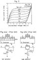
- Figs. 4(a) and 4(b) show schematic cross sections of MOSFETs of prior art Example 1 and their equivalent circuits.
- Fig. 4(a) shows a schematic cross section of a SOI NMOSFET and its equivalent circuit
- Fig. 4(b) shows a schematic cross section of a Bulk NMOSFET and its equivalent circuit.
- the equivalent circuits shown in Figs. 4(a) and 4(b) show a parasitic bipolar NPN transistor and include an impact ionization current generator Ii.
- the bipolar transistor base terminal B is tied to the substrate terminal B, the substrate/source junction is reverse biased and, as a result, the bipolar transistor has very little effect on the MOSFET operation.
- the parasitic bipolar base is the transistor body (floating).
- impact ionization current generated at the drain junction could act as a base current for the parasitic bipolar transistor, creating a positive feedback effect and degrading device electrical characteristics, specially short-channel effect and reduction of the drain/source breakdown voltage.
- This parasitic bipolar effect imposes a serious limitation for device integration.
- drain/source breakdown voltage of approximately BVdss ⁇ 2.5 V is typical.
- the maximum supply voltage should be Vddmax ⁇ 2 V. This limitation prevents the use of these SOI MOSFETs for Vdd ⁇ 3 V.
- the method involves constructing the SOI MOSFETs on thicker top Si film and using body contacts to tie the channel region to a fixed potential. This behaves as a bulk Si device suppressing the floating body effect and the parasitic bipolar effect, thereby preventing the decrease in the breakdown voltage between the source and the drain.
- Figs. 5(a) shows a schematic cross section of the MOSFET according to the prior art Example 2; and Fig. 5(b) is a graph showing drain current-voltage characteristics.
- This device can be described by the series connection of two SOI MOSFETs with the common drain (13 in Fig. 5(a)) electrically floating. The channel length of each MOSFET is d, as indicated in Fig. 5(a).
- the device comprises an active layer on an insulator film 12 formed on a silicon substrate 11.
- the active layer comprises an N-type active region (floating N-type region) 13 and P-type active regions 14, 15 sandwiching this N-type active region 13.
- the carriers bearing the P-type are injected into the N-type active region 13. Since the impurity concentration of the N-type active region 13 typically is lower by four orders of magnitude than that of the N-type source region 18, the amount of reverse-injected N-type carriers is extremely suppressed.
- the reference numerals 17, 20, 21, 22 represent a gate electrode, an insulator film, a source electrode, and a drain electrode, respectively.
- Figs. 6(a) to 6(d) are views showing a schematic cross section, a layout, and drain current-voltage characteristics of the MOSFET according to the prior art Example 3. Basically, two transistors are connected in series, then electrically, this configuration is equivalent to that of the MOSFET shown in Fig. 5(a).
- Fig. 6(a) is a view showing a schematic cross section of the dual device in which two NMOSFETs are connected in series.
- Fig. 6(b) is a plan view showing a layout of the dual device.
- Fig. 6(c) is a view showing drain current-voltage characteristics of a single device (in dotted line) and drain current-voltage characteristics of a dual device (in solid line).
- the "kink” effect is a sudden increase in the drain saturation current Id at a certain source-drain voltage Vds relative to the input gate voltage Vgs, as shown by the drain current-voltage characteristics in dotted line of Fig. 6(c).
- the “kink” effect appears when the top channel adjacent to the drain enters the source-drain punchthrough regime.
- the present invention has been made in view of the above-described circumstances and the purpose thereof is to provide a SOI MOS field effect transistor which, for example, increases the breakdown voltage between the source and drain regions, suppresses the kink effect in the drain current-voltage characteristics, and reduces the device area, and which is applicable to highly integrated circuits.
- the present invention provides a SOI MOS field effect transistor comprising: a superficial top semiconductor layer of a first conductivity type formed on a SOI substrate; source and drain regions of a second conductivity type arranged apart from each other on the top semiconductor layer; a P-type first channel region, an N + -type floating region, and a P-type second channel region formed in this order in a self-aligned manner and disposed between the N + -type source region and the N + -type drain region for an N-type MOSFET, or an N-type first channel region, a P + -type floating region, and an N-type second channel region formed in this order in a self-aligned manner and disposed between the P + -type source region and the P + -type drain region for a P-type MOSFET; and two gate electrodes for controlling the first and second channel regions, wherein a doping concentration of the second channel region adjacent to the drain region is lower than a doping concentration of the first channel region adjacent to the source region.
- the present invention provides a SOI MOS field effect transistor that increases the breakdown voltage between the source and drain regions and suppresses the kink effect in the drain current-voltage characteristics.
- the breakdown voltage between the drain and source regions can be increased by constructing the SOI MOS field effect transistor with a dual transistor having two channel regions. Further, the kink effect in the drain current-voltage characteristics (Id-Vds characteristics) is suppressed by allowing the concentration of the second channel region adjacent to the drain region to be lower than the concentration of the first channel region adjacent to the source region.
- the threshold voltage Vth2 of the second channel region is lower than the threshold voltage Vth1 of the first channel region by adjusting the doping concentrations of the first and second channel regions. This structure suppresses the "kink" effect in the drain current-voltage characteristics.
- the ratio Vth1/Vth2 of the threshold voltage Vth1 of the first channel region relative to the threshold voltage Vth2 of the second channel region is more than 4. This structure eliminates the "kink" effect in the drain current-voltage characteristics.
- the second channel region comprises an undoped channel of intrinsic-type.
- This structure allows the threshold voltage Vth2 of the second channel region to be lower than the threshold voltage Vth1 of the first channel region by setting the doping concentration of the second channel region to be, for example, less than 1 ⁇ 10 14 cm -3 and forming the first channel region at an ordinary doping concentration of about 2 ⁇ 10 17 cm -3 (boron).
- the channel lengths of the first and second channel regions are the same.
- This structure realizes a SOI MOSFET in a smaller device area than the previous art by allowing the channel lengths of the first and second channel regions to be of the same minimum size.
- Fig. 1 is a view showing a schematic cross section of a field effect transistor on SOI substrate in accordance with an embodiment of the present invention.
- the field effect transistor is formed on a SOI substrate composed of a substrate 1, a buried oxide 2 of thickness Tbox (typically between 50 nm and 500 nm), and a top Si layer 3, where an active transistor is formed.
- the MOS field effect transistor has gate electrodes 4a and 4b formed of a polysilicon or a refractory metal like MoSi 2 (molybdenum silicon), WSi 2 (tungsten silicon). Source 5 and drain 6 regions are highly doped to reduce interconnect resistance.
- the source 5 and drain 6 regions are formed as N + type.
- a P-type first channel region 7, an N + -type floating region 9, and an i-type second channel region 8 are formed in this order in a self-aligned manner and disposed between the N + type source 5 and drain 6 regions.
- the source 5 and drain 6 regions are formed as P + type.
- An N-type first channel region 7, a P + -type floating region 9, and an i-type second channel region 8 are formed in this order in a self-aligned manner and disposed between the P + type source 5 and drain 6 regions.
- the gate electrode is split into two gate electrodes 4a and 4b, as shown in Fig. 1.
- the split-gate electrodes 4a and 4b control the two channel regions 7 and 8, which are separated by the floating region 9 of the same conductivity type as the source 5 and drain 6 regions.
- the channel region 7 adjacent to the source region 5 is of the opposite conductivity of the source region 5 (P-type in the case of an N-type MOSFET). Typically, doping level in the channel region 7 is about 2 ⁇ 10 17 cm -3 (boron).
- the channel region 8 adjacent to the drain region 6 is non-doped, of intrinsic type (i-type), or very low doped, as compared with the channel region 7. Typically, doping level in the channel region 8 is less than 1 ⁇ 10 14 cm -3 .
- the floating region 9 is formed in a self-aligned manner with the source 5 and drain 6 regions.
- the doping level is the same and is 1 ⁇ 10 20 cm -3 .
- the width of the floating region 9 is about 0.4 ⁇ m. Since the structure of the MOSFET is formed in a self-aligned manner, the impurity hardly diffuses laterally, so that the device characteristics are well controlled and reproducible.
- this device structure bahaves as a series connection of two MOSFETs. In this sense it is similar to SOI MOSFETs proposed in the prior art Example 2 of Fig. 5 and the prior art Example 3 of Fig. 6. However, the MOSFET according to this embodiment is constructed as follows.
- the saturation current Idsat1 of the T1 transistor must be smaller than the saturation current Idsat2 of the T2 transistor adjacent to the drain: Idsat2 > Idsat1.
- Figs. 2(a) and 2(b) are views showing a relationship between the kink current Ik and the threshold voltage ratio Vth1/Vth2 in the SOI MOSFET according to this embodiment of the present invention.
- the threshold voltages Vth1 and Vth2 of the channel regions 7 and 8 should satisfy the relation: Vth1 > Vth2, and the threshold voltage ratio Vth1/Vth2 of more than 4 is particularly effective in reducing the kink current Ik.
- Fig. 3 is a view showing the drain current-voltage characteristics in the SOI MOSFET according to this embodiment of the present invention.
- the channel region 7 adjacent to the source region 5 is doped at a concentration of about 2 ⁇ 10 17 cm -3 (boron), while the channel region 8 adjacent to the drain region 6 is undoped or of intrinsic type. This provides that the channel region 8 (half transistor) adjacent to the drain region 6 is driven by a larger current than the channel region 7 (half transistor) adjacent to the source region 5.
- the above structure provides a SOI MOS field effect transistor having dual-doped channel regions which are controlled by different gate electrode potentials.
- a key feature is the low-doped channel region adjacent to the drain terminal, and the adjustment of the doping concentration of the channel region adjacent to the source in order to suppress the "kink" current effect without reducing the driving current.
- This structure allows to realize a transistor with high source-drain punchthrough voltage and attains high driving current in a smaller device area than the previous art.
- this transistor structure is useful to realize a high voltage interface circuitry necessary in general IC applications.
- the full advantage of the low-voltage SOI circuit, and the I/O circuits can be optimized independently.
- the device characteristics have good reproducibility, since each region in the MOSFET is formed in a self-aligned manner, without controlling the width by lateral diffusion.
- the present invention increases the breakdown voltage between the source and drain regions by forming two channel regions between the source and drain regions, and suppresses the kink effect in the drain current-voltage characteristics by controlling the doping concentrations of the two channel regions to adjust the threshold voltages in the two channel regions.
Landscapes
- Thin Film Transistor (AREA)
Applications Claiming Priority (3)
| Application Number | Priority Date | Filing Date | Title |
|---|---|---|---|
| JP00787397A JP3353875B2 (ja) | 1997-01-20 | 1997-01-20 | Soi・mos電界効果トランジスタ |
| JP7873/97 | 1997-01-20 | ||
| JP787397 | 1997-01-20 |
Publications (2)
| Publication Number | Publication Date |
|---|---|
| EP0854519A1 true EP0854519A1 (de) | 1998-07-22 |
| EP0854519B1 EP0854519B1 (de) | 2003-09-03 |
Family
ID=11677752
Family Applications (1)
| Application Number | Title | Priority Date | Filing Date |
|---|---|---|---|
| EP97309755A Expired - Lifetime EP0854519B1 (de) | 1997-01-20 | 1997-12-03 | SOI-MOS-Feldeffekttransistor |
Country Status (6)
| Country | Link |
|---|---|
| US (1) | US6204534B1 (de) |
| EP (1) | EP0854519B1 (de) |
| JP (1) | JP3353875B2 (de) |
| KR (1) | KR100297666B1 (de) |
| DE (1) | DE69724578T2 (de) |
| TW (1) | TW379452B (de) |
Cited By (3)
| Publication number | Priority date | Publication date | Assignee | Title |
|---|---|---|---|---|
| SG85660A1 (en) * | 1998-08-07 | 2002-01-15 | Ibm | Method and improved soi body contact structure for transistors |
| US6609214B1 (en) | 1999-08-23 | 2003-08-19 | International Business Machines Corporation | Method, system and program products for copying coupling facility structures |
| US7940706B2 (en) | 2001-10-01 | 2011-05-10 | International Business Machines Corporation | Controlling the state of duplexing of coupling facility structures |
Families Citing this family (16)
| Publication number | Priority date | Publication date | Assignee | Title |
|---|---|---|---|---|
| JP3408762B2 (ja) * | 1998-12-03 | 2003-05-19 | シャープ株式会社 | Soi構造の半導体装置及びその製造方法 |
| FR2789519B1 (fr) * | 1999-02-05 | 2003-03-28 | Commissariat Energie Atomique | Transistor mos a tension de seuil dynamique equipe d'un limiteur de courant, et procede de realisation d'un tel transistor |
| US6512504B1 (en) | 1999-04-27 | 2003-01-28 | Semiconductor Energy Laborayory Co., Ltd. | Electronic device and electronic apparatus |
| US8853696B1 (en) * | 1999-06-04 | 2014-10-07 | Semiconductor Energy Laboratory Co., Ltd. | Electro-optical device and electronic device |
| JP5210473B2 (ja) * | 1999-06-21 | 2013-06-12 | 株式会社半導体エネルギー研究所 | 表示装置 |
| US6414340B1 (en) | 1999-11-04 | 2002-07-02 | Raytheon Company | Field effect transistor and method for making the same |
| US7112844B2 (en) | 2001-04-19 | 2006-09-26 | Semiconductor Energy Laboratory Co., Ltd. | Semiconductor device and manufacturing method thereof |
| KR20110113215A (ko) * | 2004-06-09 | 2011-10-14 | 르네사스 일렉트로닉스 가부시키가이샤 | 반도체 기억 장치 |
| US20070210380A1 (en) * | 2006-03-10 | 2007-09-13 | Jin-Yuan Lee | Body connection structure for soi mos transistor |
| JP2007287945A (ja) * | 2006-04-18 | 2007-11-01 | Mitsubishi Electric Corp | 薄膜トランジスタ |
| TW200805866A (en) * | 2006-07-04 | 2008-01-16 | Powertech Ind Ltd | Charger for current socket and power transmission method |
| JP2008135605A (ja) * | 2006-11-29 | 2008-06-12 | Seiko Epson Corp | 半導体装置および電気光学装置 |
| TWI319625B (en) * | 2006-11-30 | 2010-01-11 | Tpo Displays Corp | Image display system and manufacturing method of multi-gates thin film transistor |
| WO2010151857A2 (en) * | 2009-06-26 | 2010-12-29 | Cornell University | Method for forming iii-v semiconductor structures including aluminum-silicon nitride passivation |
| US9741857B2 (en) * | 2015-08-07 | 2017-08-22 | Ahmad Tarakji | Approach for an area-efficient and scalable CMOS performance based on advanced Silicon-On-Insulator (SOI), Silicon-On-Sapphire (SOS) and Silicon-On-Nothing (SON) technologies |
| US10714623B2 (en) * | 2015-08-07 | 2020-07-14 | Ahmad Houssam Tarakji | Approach for an area-efficient and scalable CMOS performance based on advanced silicon-on-insulator (SOI), silicon-on-sapphire (SOS) and silicon-on-nothing (SON) technologies |
Citations (3)
| Publication number | Priority date | Publication date | Assignee | Title |
|---|---|---|---|---|
| EP0359528A2 (de) * | 1988-09-16 | 1990-03-21 | Xerox Corporation | Hochspannungsdünnschichttransistoren |
| EP0449351A1 (de) * | 1990-03-28 | 1991-10-02 | Interuniversitair Microelektronica Centrum Vzw | Schaltungselement zum Verhindern des Kink-Effekts |
| EP0586735A1 (de) * | 1987-09-28 | 1994-03-16 | Siemens Aktiengesellschaft | MOS-Transistor |
Family Cites Families (10)
| Publication number | Priority date | Publication date | Assignee | Title |
|---|---|---|---|---|
| JPS5433679A (en) * | 1977-08-22 | 1979-03-12 | Agency Of Ind Science & Technol | Semiconductor intergrated circuit on insulation substrate |
| US4845047A (en) * | 1987-06-25 | 1989-07-04 | Texas Instruments Incorporated | Threshold adjustment method for an IGFET |
| US5245207A (en) * | 1989-04-21 | 1993-09-14 | Nobuo Mikoshiba | Integrated circuit |
| US5272369A (en) * | 1990-03-28 | 1993-12-21 | Interuniversitair Micro-Elektronica Centrum Vzw | Circuit element with elimination of kink effect |
| DE69128876T2 (de) * | 1990-11-30 | 1998-08-06 | Sharp Kk | Dünnfilm-Halbleitervorrichtung |
| JPH04241466A (ja) * | 1991-01-16 | 1992-08-28 | Casio Comput Co Ltd | 電界効果型トランジスタ |
| JPH05218425A (ja) | 1992-01-31 | 1993-08-27 | Nippon Telegr & Teleph Corp <Ntt> | 電界効果型半導体装置およびその製造方法 |
| JPH0661454A (ja) * | 1992-08-10 | 1994-03-04 | Hitachi Ltd | 半導体集積回路装置 |
| KR0161398B1 (ko) * | 1995-03-13 | 1998-12-01 | 김광호 | 고내압 트랜지스터 및 그 제조방법 |
| JP3222380B2 (ja) * | 1996-04-25 | 2001-10-29 | シャープ株式会社 | 電界効果トランジスタ、および、cmosトランジスタ |
-
1997
- 1997-01-20 JP JP00787397A patent/JP3353875B2/ja not_active Expired - Fee Related
- 1997-12-03 EP EP97309755A patent/EP0854519B1/de not_active Expired - Lifetime
- 1997-12-03 US US08/984,083 patent/US6204534B1/en not_active Expired - Fee Related
- 1997-12-03 TW TW86118190A patent/TW379452B/zh not_active IP Right Cessation
- 1997-12-03 DE DE69724578T patent/DE69724578T2/de not_active Expired - Lifetime
- 1997-12-31 KR KR1019970080790A patent/KR100297666B1/ko not_active Expired - Fee Related
Patent Citations (3)
| Publication number | Priority date | Publication date | Assignee | Title |
|---|---|---|---|---|
| EP0586735A1 (de) * | 1987-09-28 | 1994-03-16 | Siemens Aktiengesellschaft | MOS-Transistor |
| EP0359528A2 (de) * | 1988-09-16 | 1990-03-21 | Xerox Corporation | Hochspannungsdünnschichttransistoren |
| EP0449351A1 (de) * | 1990-03-28 | 1991-10-02 | Interuniversitair Microelektronica Centrum Vzw | Schaltungselement zum Verhindern des Kink-Effekts |
Non-Patent Citations (2)
| Title |
|---|
| CEUSTER DE D ET AL: "KINK-LIKE EFFECT IN LONG N-CHANNEL TWIN-GATE FULLY-DIPLETED SOI MOSFETS", ELECTRONICS LETTERS, vol. 30, no. 17, 18 August 1994 (1994-08-18), pages 1456 - 1458, XP000476054 * |
| J.P. COLINGE ET AL., IEEE ELETCRON DEVICE LETTERS, vol. edl-7, no. 12, December 1986 (1986-12-01), pages 697 - 699, XP000002221 * |
Cited By (8)
| Publication number | Priority date | Publication date | Assignee | Title |
|---|---|---|---|---|
| SG85660A1 (en) * | 1998-08-07 | 2002-01-15 | Ibm | Method and improved soi body contact structure for transistors |
| US9253046B2 (en) | 1998-09-10 | 2016-02-02 | International Business Machines Corporation | Controlling the state of duplexing of coupling facility structures |
| US9565013B2 (en) | 1998-09-10 | 2017-02-07 | International Business Machines Corporation | Controlling the state of duplexing of coupling facility structures |
| US9860315B2 (en) | 1998-09-10 | 2018-01-02 | International Business Machines Corporation | Controlling the state of duplexing of coupling facility structures |
| US6609214B1 (en) | 1999-08-23 | 2003-08-19 | International Business Machines Corporation | Method, system and program products for copying coupling facility structures |
| US7940706B2 (en) | 2001-10-01 | 2011-05-10 | International Business Machines Corporation | Controlling the state of duplexing of coupling facility structures |
| US8341188B2 (en) | 2001-10-01 | 2012-12-25 | International Business Machines Corporation | Controlling the state of duplexing of coupling facility structures |
| US10491675B2 (en) | 2001-10-01 | 2019-11-26 | International Business Machines Corporation | Controlling the state of duplexing of coupling facility structures |
Also Published As
| Publication number | Publication date |
|---|---|
| DE69724578D1 (de) | 2003-10-09 |
| US6204534B1 (en) | 2001-03-20 |
| KR100297666B1 (ko) | 2001-10-25 |
| KR19980070304A (ko) | 1998-10-26 |
| EP0854519B1 (de) | 2003-09-03 |
| DE69724578T2 (de) | 2004-07-29 |
| JPH10209456A (ja) | 1998-08-07 |
| JP3353875B2 (ja) | 2002-12-03 |
| TW379452B (en) | 2000-01-11 |
Similar Documents
| Publication | Publication Date | Title |
|---|---|---|
| US6204534B1 (en) | SOI MOS field effect transistor | |
| JP3504212B2 (ja) | Soi構造の半導体装置 | |
| US6930361B2 (en) | Semiconductor device realizing characteristics like a SOI MOSFET | |
| US5146298A (en) | Device which functions as a lateral double-diffused insulated gate field effect transistor or as a bipolar transistor | |
| US5821575A (en) | Compact self-aligned body contact silicon-on-insulator transistor | |
| EP0803911B1 (de) | Kanalstruktur eines Feldeffekttransistors und eines CMOS-Elements | |
| US9117893B1 (en) | Tunneling transistor suitable for low voltage operation | |
| US6232642B1 (en) | Semiconductor device having impurity region locally at an end of channel formation region | |
| US5672995A (en) | High speed mis-type intergrated circuit with self-regulated back bias | |
| US6963100B2 (en) | Semiconductor device having gate electrode in which depletion layer can be generated | |
| US6770517B2 (en) | Semiconductor device and method for fabricating the same | |
| US6288425B1 (en) | SOI-MOSFET device | |
| US6462379B2 (en) | SOI semiconductor device and method for manufacturing the same | |
| JPH11233788A (ja) | 半導体装置 | |
| JP4679146B2 (ja) | 電界効果トランジスタ | |
| US6627505B2 (en) | Method of producing SOI MOSFET having threshold voltage of central and edge regions in opposite directions | |
| US7282763B2 (en) | Field effect transistor formed on an insulating substrate and integrated circuit thereof | |
| CN100353510C (zh) | 绝缘栅薄膜晶体管及其控制系统 | |
| JP3230184B2 (ja) | 半導体装置の製造方法 | |
| US20030203544A1 (en) | CMOS transistor on thin silicon-on-insulator using accumulation as conduction mechanism |
Legal Events
| Date | Code | Title | Description |
|---|---|---|---|
| PUAI | Public reference made under article 153(3) epc to a published international application that has entered the european phase |
Free format text: ORIGINAL CODE: 0009012 |
|
| AK | Designated contracting states |
Kind code of ref document: A1 Designated state(s): DE FR GB IT NL |
|
| AX | Request for extension of the european patent |
Free format text: AL;LT;LV;MK;RO;SI |
|
| 17P | Request for examination filed |
Effective date: 19981021 |
|
| AKX | Designation fees paid |
Free format text: DE FR GB IT NL |
|
| RBV | Designated contracting states (corrected) |
Designated state(s): DE FR GB IT NL |
|
| 17Q | First examination report despatched |
Effective date: 20020416 |
|
| GRAH | Despatch of communication of intention to grant a patent |
Free format text: ORIGINAL CODE: EPIDOS IGRA |
|
| GRAH | Despatch of communication of intention to grant a patent |
Free format text: ORIGINAL CODE: EPIDOS IGRA |
|
| GRAA | (expected) grant |
Free format text: ORIGINAL CODE: 0009210 |
|
| AK | Designated contracting states |
Kind code of ref document: B1 Designated state(s): DE FR GB IT NL |
|
| REG | Reference to a national code |
Ref country code: GB Ref legal event code: FG4D |
|
| REF | Corresponds to: |
Ref document number: 69724578 Country of ref document: DE Date of ref document: 20031009 Kind code of ref document: P |
|
| ET | Fr: translation filed | ||
| PLBE | No opposition filed within time limit |
Free format text: ORIGINAL CODE: 0009261 |
|
| STAA | Information on the status of an ep patent application or granted ep patent |
Free format text: STATUS: NO OPPOSITION FILED WITHIN TIME LIMIT |
|
| 26N | No opposition filed |
Effective date: 20040604 |
|
| PGFP | Annual fee paid to national office [announced via postgrant information from national office to epo] |
Ref country code: FR Payment date: 20101224 Year of fee payment: 14 |
|
| PGFP | Annual fee paid to national office [announced via postgrant information from national office to epo] |
Ref country code: IT Payment date: 20101218 Year of fee payment: 14 Ref country code: NL Payment date: 20101220 Year of fee payment: 14 Ref country code: GB Payment date: 20101201 Year of fee payment: 14 |
|
| PGFP | Annual fee paid to national office [announced via postgrant information from national office to epo] |
Ref country code: DE Payment date: 20101130 Year of fee payment: 14 |
|
| REG | Reference to a national code |
Ref country code: NL Ref legal event code: V1 Effective date: 20120701 |
|
| GBPC | Gb: european patent ceased through non-payment of renewal fee |
Effective date: 20111203 |
|
| REG | Reference to a national code |
Ref country code: FR Ref legal event code: ST Effective date: 20120831 |
|
| REG | Reference to a national code |
Ref country code: DE Ref legal event code: R119 Ref document number: 69724578 Country of ref document: DE Effective date: 20120703 |
|
| PG25 | Lapsed in a contracting state [announced via postgrant information from national office to epo] |
Ref country code: DE Free format text: LAPSE BECAUSE OF NON-PAYMENT OF DUE FEES Effective date: 20120703 Ref country code: GB Free format text: LAPSE BECAUSE OF NON-PAYMENT OF DUE FEES Effective date: 20111203 |
|
| PG25 | Lapsed in a contracting state [announced via postgrant information from national office to epo] |
Ref country code: IT Free format text: LAPSE BECAUSE OF NON-PAYMENT OF DUE FEES Effective date: 20111203 |
|
| PG25 | Lapsed in a contracting state [announced via postgrant information from national office to epo] |
Ref country code: NL Free format text: LAPSE BECAUSE OF NON-PAYMENT OF DUE FEES Effective date: 20120701 |
|
| PG25 | Lapsed in a contracting state [announced via postgrant information from national office to epo] |
Ref country code: FR Free format text: LAPSE BECAUSE OF NON-PAYMENT OF DUE FEES Effective date: 20120102 |