EP0854562A1 - Alimentation de puissance à decoupape - Google Patents
Alimentation de puissance à decoupape Download PDFInfo
- Publication number
- EP0854562A1 EP0854562A1 EP97121973A EP97121973A EP0854562A1 EP 0854562 A1 EP0854562 A1 EP 0854562A1 EP 97121973 A EP97121973 A EP 97121973A EP 97121973 A EP97121973 A EP 97121973A EP 0854562 A1 EP0854562 A1 EP 0854562A1
- Authority
- EP
- European Patent Office
- Prior art keywords
- switched
- power supply
- mode power
- resistor
- supply according
- Prior art date
- Legal status (The legal status is an assumption and is not a legal conclusion. Google has not performed a legal analysis and makes no representation as to the accuracy of the status listed.)
- Granted
Links
- 238000003860 storage Methods 0.000 claims abstract description 15
- 239000003990 capacitor Substances 0.000 claims description 20
- 230000001681 protective effect Effects 0.000 claims description 10
- 238000011144 upstream manufacturing Methods 0.000 claims description 3
- 238000007599 discharging Methods 0.000 claims 1
- 238000012432 intermediate storage Methods 0.000 abstract 1
- 238000010586 diagram Methods 0.000 description 3
- 230000006870 function Effects 0.000 description 3
- 238000004804 winding Methods 0.000 description 3
- 238000004146 energy storage Methods 0.000 description 2
- 230000001105 regulatory effect Effects 0.000 description 2
- 230000000903 blocking effect Effects 0.000 description 1
- 230000006378 damage Effects 0.000 description 1
- 230000000694 effects Effects 0.000 description 1
- 230000005669 field effect Effects 0.000 description 1
- 238000009472 formulation Methods 0.000 description 1
- 238000009413 insulation Methods 0.000 description 1
- 238000005259 measurement Methods 0.000 description 1
- 239000000203 mixture Substances 0.000 description 1
- 238000012216 screening Methods 0.000 description 1
- 238000010792 warming Methods 0.000 description 1
- 229910000859 α-Fe Inorganic materials 0.000 description 1
Images

Classifications
-
- H—ELECTRICITY
- H03—ELECTRONIC CIRCUITRY
- H03K—PULSE TECHNIQUE
- H03K17/00—Electronic switching or gating, i.e. not by contact-making and –breaking
- H03K17/51—Electronic switching or gating, i.e. not by contact-making and –breaking characterised by the components used
- H03K17/78—Electronic switching or gating, i.e. not by contact-making and –breaking characterised by the components used using opto-electronic devices, i.e. light-emitting and photoelectric devices electrically- or optically-coupled
- H03K17/785—Electronic switching or gating, i.e. not by contact-making and –breaking characterised by the components used using opto-electronic devices, i.e. light-emitting and photoelectric devices electrically- or optically-coupled controlling field-effect transistor switches
-
- H—ELECTRICITY
- H02—GENERATION; CONVERSION OR DISTRIBUTION OF ELECTRIC POWER
- H02M—APPARATUS FOR CONVERSION BETWEEN AC AND AC, BETWEEN AC AND DC, OR BETWEEN DC AND DC, AND FOR USE WITH MAINS OR SIMILAR POWER SUPPLY SYSTEMS; CONVERSION OF DC OR AC INPUT POWER INTO SURGE OUTPUT POWER; CONTROL OR REGULATION THEREOF
- H02M3/00—Conversion of DC power input into DC power output
- H02M3/02—Conversion of DC power input into DC power output without intermediate conversion into AC
- H02M3/04—Conversion of DC power input into DC power output without intermediate conversion into AC by static converters
- H02M3/10—Conversion of DC power input into DC power output without intermediate conversion into AC by static converters using discharge tubes with control electrode or semiconductor devices with control electrode
- H02M3/145—Conversion of DC power input into DC power output without intermediate conversion into AC by static converters using discharge tubes with control electrode or semiconductor devices with control electrode using devices of a triode or transistor type requiring continuous application of a control signal
- H02M3/155—Conversion of DC power input into DC power output without intermediate conversion into AC by static converters using discharge tubes with control electrode or semiconductor devices with control electrode using devices of a triode or transistor type requiring continuous application of a control signal using semiconductor devices only
- H02M3/156—Conversion of DC power input into DC power output without intermediate conversion into AC by static converters using discharge tubes with control electrode or semiconductor devices with control electrode using devices of a triode or transistor type requiring continuous application of a control signal using semiconductor devices only with automatic control of output voltage or current, e.g. switching regulators
- H02M3/1563—Conversion of DC power input into DC power output without intermediate conversion into AC by static converters using discharge tubes with control electrode or semiconductor devices with control electrode using devices of a triode or transistor type requiring continuous application of a control signal using semiconductor devices only with automatic control of output voltage or current, e.g. switching regulators without using an external clock
-
- H—ELECTRICITY
- H03—ELECTRONIC CIRCUITRY
- H03K—PULSE TECHNIQUE
- H03K17/00—Electronic switching or gating, i.e. not by contact-making and –breaking
- H03K17/04—Modifications for accelerating switching
- H03K17/041—Modifications for accelerating switching without feedback from the output circuit to the control circuit
- H03K17/0412—Modifications for accelerating switching without feedback from the output circuit to the control circuit by measures taken in the control circuit
- H03K17/04123—Modifications for accelerating switching without feedback from the output circuit to the control circuit by measures taken in the control circuit in field-effect transistor switches
Definitions
- the present invention relates to a switching power supply clocked switching regulator, being an electronic switching element periodically in a certain duty cycle that is turned on and off from a rectified Input voltage via a memory circuit with a storage choke, an intermediate circuit storage capacitor and a freewheeling diode an output control voltage is produced.
- switching power supplies are sufficient known. Your advantages are: relatively high efficiency, relatively low screening effort due to high clock frequency, high Input voltage range; the disadvantages: use of special, sometimes very expensive components (including special Storage chokes with special ferrite and, if necessary, at least two windings), control circuit required. Because of the disadvantages mentioned, such switching power supplies - especially for economic reasons - not yet used for all applications where they are used in technical In principle, would be well suited.
- the present invention is therefore based on the object to create a switching power supply of the type mentioned by a significant reduction in the cost anyway at least satisfactory efficiency and sufficient high output power for a wider range of applications suitable is.
- this is achieved in that the switching element from a transistor, namely a field effect transistor (FET) or an IGBT (Insulated Gate Bipolar Transistor), is formed, the base or gate of which special control circuit is connected upstream in such a way that in the control circuit for switching the switching element briefly an increased control current and subsequently a significantly lower one when switched on Holding current flows.
- FET field effect transistor
- IGBT Insulated Gate Bipolar Transistor
- the invention is based on the knowledge that the electronic Switching element (FET / IGBT) for switching through a relatively high control energy (start-up charge) is required because between the main current path (drain / source) and the base or the gate have very large internal capacities, and that Switching element can only conduct (switch through) so quickly, how these inner capacities are charged. It must therefore be ensured that in the control circuit sufficient within a very short time (a few ⁇ s) high current can flow.
- the Ballast resistor designed according to low resistance e.g. for a current of at least 30 mA at 230 V), which makes it for a very high power loss should be interpreted (strong warming).
- the present invention achieves that the series resistor circuit as a whole, i.e. in total, can be relatively high impedance, so that normally, i.e. in the switched-through state of the switching element, including the Current - as holding current - is insignificantly low.
- Control circuit briefly a high control current generated practically as an amplified current pulse, so that it is, so to speak, a "drive pulse amplifier" acts.
- a capacitor is preferably used as an energy store used for a short time (at least) a part of a preferably designed as a voltage divider Series resistor circuit in the gate-driving current or Resistance path bridged.
- the invention advantageously means that no "active" Circuit for generating an auxiliary voltage required. Rather, the circuit according to the invention predominantly comes with passive and therefore very inexpensive components. For the resistors of the series resistor circuit can because of the very low power uses cheap resistance classes will. As the (only) active component of the invention Drive circuit can be a very inexpensive Switching transistor (e.g. BSR 19) can be used.
- BSR 19 Switching transistor
- the electronic switching element together with a flip-flop transistor forms, this flip-flop via a control resistor current controlled - and therefore advantageously short-circuit proof - is and controlled by a control signal becomes.
- the breakover transistor can also be a very inexpensive Small signal transistor (e.g. BC 847) can be used.
- the control signal from the side is preferred the output control voltage potential-free - in particular via an optocoupler - in the control loop of the switching regulator fed back. This will make a second, very expensive Winding saved on the storage inductor, so that a very inexpensive storage choke with only one winding and therefore very little insulation effort is used can be (rod or ring choke).
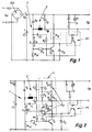
- an AC voltage on the input side is rectified via a rectifier GR and preferably smoothed by a parallel capacitor C 1 ; a rectified input voltage U E is produced , from which an output regulating voltage U B is generated by means of a clocked switching regulator 1.
- an electronic switching element T 1 is periodically switched on and off in a certain clock ratio corresponding to the desired control voltage.
- the switching element T 1 interacts with a storage circuit 2, which consists of a storage inductor L, an intermediate circuit storage capacitor C Z and a free-wheeling diode D F.
- a storage circuit 2 which consists of a storage inductor L, an intermediate circuit storage capacitor C Z and a free-wheeling diode D F.
- the switching element T 1 is an FET in the embodiment shown, the source connection S of which is connected to the negative line "-" via a control resistor R M and the drain connection D of which is connected to the storage inductor L and the free-wheeling diode D F is connected to the positive line "+" connected is.
- the other connection of the storage inductor L forms the minus line -U B of the output control voltage U B.
- the storage capacitor C Z lies between the positive line and -U B.
- the gate connection G of the switching element T 1 is preceded by a series resistor circuit R G consisting of only a single resistor. As already explained at the beginning, this individual resistor would have to be designed with very low resistance and therefore for high performance.
- a special control circuit 4 is therefore provided according to the invention at this point, which is framed with a dashed line and is thus emphasized.
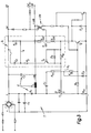
- the series resistor circuit R G is formed as a voltage divider from at least two, according to FIG. 2, from three individual resistors R G1 , R G2 and R B.
- the base-emitter path of a drive transistor T 3 is parallel to the last-mentioned individual resistor R B , the resistor R B being designed in such a way that when there is a current flow across the entire series resistor circuit at R B, a voltage drops with a level (for example in the range from 0.7 to 2 V), so that the control transistor T 3 can turn on.
- the control transistor T 3 lies with its main current path, its collector-emitter path, in a secondary branch parallel to the series resistor circuit R G.
- a protective resistor R 3 and - as an energy store - a capacitor C 3 are arranged in series between the collector and the positive line.
- the point between the individual resistors R G1 and R G2 of the series resistor circuit is preferably connected to the point between the capacitor C 3 and the protective resistor R 3 via a cross connection 6.
- a discharge diode D 3 is parallel to the base-emitter path of the drive transistor T 3 and to the individual resistor R B parallel to it.
- the electronic switching element T 1 together with a second transistor T 2 , here called a toggle transistor, forms a toggle circuit which is current-controlled via the control resistor R M - and therefore advantageously short-circuit proof.
- the flip-flop T 1 / T 2 is controlled via a control or regulating signal X.
- This control signal X is advantageously potential-free fed back into the control circuit of the switching regulator from the side of the output control voltage U B, in particular via an optocoupler OK.
- the optocoupler OK is connected on the primary side to -U B on the one hand and on the other hand to the positive lead via a resistor and a Zener diode.
- the control signal X is derived here; 1 and 2, this is illustrated in simplified form by a potentiometer.
- the optocoupler is OK on the one hand with the base of the toggle transistor T 2 and on the other hand preferably with a voltage divider tap between two individual resistors (according to FIGS. 1 and 2 R G2 and R B or according to FIG. 3 R G21 and R G22 ) of the series resistor circuit R G connected.
- the base of the flip-flop transistor T 2 is also on the one hand via a series R / C element consisting of a resistor R T and a capacitor C T with the drain terminal D of the switching element T 1 and on the other hand - in particular via a series resistor R V - with a Switching point connected between the control resistor R M and the source terminal S of the switching element T 1 .
- the flip-flop transistor T 2 With its collector-emitter path, the flip-flop transistor T 2 lies between the gate terminal G of the switching element T 1 , preferably a voltage divider tap between two individual resistors R B and R G2 or R G22 , on the one hand, and the negative line on the other.
- a zener diode D Z is parallel to the collector-emitter path of the breakover transistor.
- the series resistor circuit R G is designed to have a relatively high resistance in the sum of the individual resistors, so that only a very small current can flow through this branch. If, at a certain point in time, the output control voltage U B falls below the setpoint, the triggering transistor T 2 is blocked via the corresponding control signal X, in order to make the switching element T 1 conductive. As a result, a very low current of, for example, only 1 to 1.5 mA flows through the series resistor circuit R G , which is completely problem-free in terms of power loss even without special measures. In this case, however, the drive transistor T 3 becomes conductive relatively quickly, due to the voltage drop at R B.
- T 3 When T 3 becomes conductive, its collector-emitter path flows in parallel to the R G branch via C 3 and R 3 (which, for example, is negligibly small at 1.5 k ⁇ and only serves to protect T 3 from short-circuits) relatively large current into gate G of T 1 .
- a high gate drive power pulse is thus available (“pulse amplifier”).
- the capacitances of the switching element T 1 are charged very quickly, so that T 1 switches through very quickly. Then this charging current flow stops and the control transistor T 3 blocks after an e-function.
- the switched-through state of T 1 is maintained in the further course via the series circuit R G , for which only an extremely small current of a few ⁇ A flows, which are completely irrelevant in terms of power loss.
- the switch-off takes place as a function of the control signal X by switching the toggle transistor T 2 .
- the gate G of the switching element T 1 is discharged via the discharge diode D 3 .
- the control or actuating signal X comes from one not shown consumer, which is why in Fig. 3 with XW is designated.
- This version is particularly suitable for feeding electric motors, e.g. Fan motors with meshed control loop.
- the control loop or Speed controller of the motor the pre-control circuit of the switching power supply so that the engine is always slightly higher Receives tension than he really needs. This is ensures that the actual engine speed control always has a sufficiently high voltage available.
- the individual resistor R G2 is again divided into two resistors R G21 and R G22 .
- the switching point between these two resistors is used to connect the secondary circuit of the optocoupler OK.
- the protective diode D S is basically ineffective; the "normal" R T / C T element acts to ensure that the flip-flop transistor T 2 becomes conductive.
- the switching element T 1 becomes conductive again, it draws current through the protective diode D S and the smaller partial resistor R T1 and thereby charges the capacitor C T.
- This measure also leads to the second advantage that unequal time constants come into effect in the time cycle.
- C T must be recharged or discharged, which takes place via the diode D S and only via the smaller resistor R T1 .
- both partial resistances R T1 + R T2 act for charging when T 2 is kept conductive.
- the invention leads primarily to the advantage of a serious cost reduction.
- the power supply unit according to the invention can be offered significantly cheaper than conventional switching power supply units of comparable performance, so that it is suitable for many applications.
- control circuit 4 to 7 are still some design variants the control circuit 4 according to the invention illustrated. All design variants have in common that (at least) a capacitor as an energy store in parallel with a discharge resistor is arranged and thus this discharge resistance temporarily bridged.
- the capacitor C 3 is parallel to the resistor R G1 and in series with the collector of the drive transistor T 3 .
- a protective resistor R ' 3 is provided here between the capacitor C 3 and the positive line, as a result of which the transistor C 3 need only be designed for a relatively low voltage.
- the collector of transistor T 3 is preceded by a parallel circuit comprising resistor R 3 and capacitor C 3 .
- the transistor T 3 would have to be designed for the full collector / emitter voltage.
- the energy storage capacitor is arranged in parallel with part of the voltage divider. 6, the capacitor C 3 is parallel to the resistor R G2 between the center tap of the voltage divider and the negative line.
- the energy storage capacitor is divided into two partial capacitances C 31 and C 32 , which form a capacitive voltage divider which is connected in parallel with the ohmic voltage divider.
- the resistor R G1 of the voltage divider also acts as a protective resistor R ' 3 for the transistor C 3 .
- the transistor C 3 must in turn be designed for the full C / E voltage.
- the invention is not based on the specifically described exemplary embodiments limited, but also includes all in For the purposes of the invention, equivalent embodiments. Further So far, the invention is not yet in the claim 1 defined combination of features limited, but can also be determined by any other combination of certain Characteristics of all of the individual characteristics disclosed be defined. This means that basically practically every single feature of claim 1 omitted or by at least one elsewhere in the registration disclosed individual feature can be replaced. To that extent claim 1 only as a first attempt at formulation to understand for an invention.
Landscapes
- Engineering & Computer Science (AREA)
- Power Engineering (AREA)
- Dc-Dc Converters (AREA)
- Amplifiers (AREA)
- Oscillators With Electromechanical Resonators (AREA)
Applications Claiming Priority (2)
| Application Number | Priority Date | Filing Date | Title |
|---|---|---|---|
| DE29621905U | 1996-12-17 | ||
| DE29621905 | 1996-12-17 |
Publications (2)
| Publication Number | Publication Date |
|---|---|
| EP0854562A1 true EP0854562A1 (fr) | 1998-07-22 |
| EP0854562B1 EP0854562B1 (fr) | 2002-10-30 |
Family
ID=8033426
Family Applications (1)
| Application Number | Title | Priority Date | Filing Date |
|---|---|---|---|
| EP97121973A Expired - Lifetime EP0854562B1 (fr) | 1996-12-17 | 1997-12-12 | Alimentation de puissance à decoupape |
Country Status (3)
| Country | Link |
|---|---|
| US (1) | US5963024A (fr) |
| EP (1) | EP0854562B1 (fr) |
| DE (2) | DE59708621D1 (fr) |
Families Citing this family (3)
| Publication number | Priority date | Publication date | Assignee | Title |
|---|---|---|---|---|
| DE10108131A1 (de) * | 2001-02-21 | 2002-09-05 | Infineon Technologies Ag | Halbleiterschaltung und Schaltnetzteil |
| EP1427095B1 (fr) * | 2002-12-02 | 2007-04-18 | ebm-papst St. Georgen GmbH & Co. KG | Moteur électrique à commutation électronique |
| WO2010019691A1 (fr) * | 2008-08-12 | 2010-02-18 | Ixys Corporation | Système et procédé de préservation de la puissance appliquée à un appareil électrique |
Citations (12)
| Publication number | Priority date | Publication date | Assignee | Title |
|---|---|---|---|---|
| GB2022943A (en) * | 1978-06-12 | 1979-12-19 | Siemens Ag | A.C. to D.C. converter |
| US4430608A (en) * | 1981-12-22 | 1984-02-07 | Hughes Aircraft Company | Base drive circuit |
| US4445055A (en) * | 1981-03-05 | 1984-04-24 | Siemens Aktiengesellschaft | Circuit arrangement for controlling a power field-effect switching transistor |
| US4471245A (en) * | 1982-06-21 | 1984-09-11 | Eaton Corporation | FET Gating circuit with fast turn-on capacitor |
| DE3403282A1 (de) * | 1984-01-31 | 1985-08-01 | Siemens AG, 1000 Berlin und 8000 München | Sekundaerschaltregler mit geringen schaltverlusten |
| US4553082A (en) * | 1984-05-25 | 1985-11-12 | Hughes Aircraft Company | Transformerless drive circuit for field-effect transistors |
| JPH0412664A (ja) * | 1990-04-28 | 1992-01-17 | Mitsubishi Electric Corp | スイッチングレギュレータ |
| JPH0426360A (ja) * | 1990-05-18 | 1992-01-29 | Mitsubishi Electric Corp | スイッチング電源回路 |
| JPH04140059A (ja) * | 1990-09-29 | 1992-05-14 | Toshiba Lighting & Technol Corp | 電源装置 |
| WO1995006972A1 (fr) * | 1993-09-02 | 1995-03-09 | Micrel, Inc. | Regulateur de commutation possedant des caracteristiques de prevention de courant eleve |
| EP0677861A2 (fr) * | 1994-04-15 | 1995-10-18 | Linear Technology Corporation | Circuit d'attaque à haute vitesse pour régulateur à découpage |
| JPH0833324A (ja) * | 1994-07-15 | 1996-02-02 | Tabuchi Denki Kk | 直流−直流変換装置 |
Family Cites Families (11)
| Publication number | Priority date | Publication date | Assignee | Title |
|---|---|---|---|---|
| EP0095724A3 (fr) * | 1982-05-26 | 1984-03-28 | Nippon Chemi-Con Corporation | Circuit de commutation |
| JPS63114567A (ja) * | 1986-10-29 | 1988-05-19 | Hitachi Metals Ltd | スイツチング電源 |
| DE3640603A1 (de) * | 1986-11-27 | 1988-06-09 | Telefonbau & Normalzeit Gmbh | Schaltungsanordnung fuer einen gleichspannungs-schaltwandler |
| DE3843260C1 (fr) * | 1988-12-22 | 1990-05-03 | Ant Nachrichtentechnik Gmbh, 7150 Backnang, De | |
| DE3908338A1 (de) * | 1989-03-15 | 1990-09-20 | Hella Kg Hueck & Co | Verfahren und einrichtung zum ansteuern einer last, insbesondere in kraftfahrzeugen |
| US5301095A (en) * | 1991-10-01 | 1994-04-05 | Origin Electric Company, Limited | High power factor AC/DC converter |
| JPH06209569A (ja) * | 1993-01-05 | 1994-07-26 | Yokogawa Electric Corp | スイッチング電源装置 |
| KR100268201B1 (ko) * | 1993-11-12 | 2000-10-16 | 사까모또히로시 | 스위칭전원장치 |
| ES2150072T3 (es) * | 1995-05-26 | 2000-11-16 | At & T Corp | Control del factor de potencia en rectificadores conmutados. |
| JP2835299B2 (ja) * | 1995-07-25 | 1998-12-14 | 東光株式会社 | 自励式dc−dcコンバータ |
| KR100199831B1 (ko) * | 1996-01-15 | 1999-06-15 | 구자홍 | 영상기기의 절전 제어회로 |
-
1997
- 1997-12-12 EP EP97121973A patent/EP0854562B1/fr not_active Expired - Lifetime
- 1997-12-12 DE DE59708621T patent/DE59708621D1/de not_active Expired - Lifetime
- 1997-12-16 DE DE29722167U patent/DE29722167U1/de not_active Expired - Lifetime
- 1997-12-17 US US08/992,302 patent/US5963024A/en not_active Expired - Fee Related
Patent Citations (12)
| Publication number | Priority date | Publication date | Assignee | Title |
|---|---|---|---|---|
| GB2022943A (en) * | 1978-06-12 | 1979-12-19 | Siemens Ag | A.C. to D.C. converter |
| US4445055A (en) * | 1981-03-05 | 1984-04-24 | Siemens Aktiengesellschaft | Circuit arrangement for controlling a power field-effect switching transistor |
| US4430608A (en) * | 1981-12-22 | 1984-02-07 | Hughes Aircraft Company | Base drive circuit |
| US4471245A (en) * | 1982-06-21 | 1984-09-11 | Eaton Corporation | FET Gating circuit with fast turn-on capacitor |
| DE3403282A1 (de) * | 1984-01-31 | 1985-08-01 | Siemens AG, 1000 Berlin und 8000 München | Sekundaerschaltregler mit geringen schaltverlusten |
| US4553082A (en) * | 1984-05-25 | 1985-11-12 | Hughes Aircraft Company | Transformerless drive circuit for field-effect transistors |
| JPH0412664A (ja) * | 1990-04-28 | 1992-01-17 | Mitsubishi Electric Corp | スイッチングレギュレータ |
| JPH0426360A (ja) * | 1990-05-18 | 1992-01-29 | Mitsubishi Electric Corp | スイッチング電源回路 |
| JPH04140059A (ja) * | 1990-09-29 | 1992-05-14 | Toshiba Lighting & Technol Corp | 電源装置 |
| WO1995006972A1 (fr) * | 1993-09-02 | 1995-03-09 | Micrel, Inc. | Regulateur de commutation possedant des caracteristiques de prevention de courant eleve |
| EP0677861A2 (fr) * | 1994-04-15 | 1995-10-18 | Linear Technology Corporation | Circuit d'attaque à haute vitesse pour régulateur à découpage |
| JPH0833324A (ja) * | 1994-07-15 | 1996-02-02 | Tabuchi Denki Kk | 直流−直流変換装置 |
Non-Patent Citations (4)
| Title |
|---|
| PATENT ABSTRACTS OF JAPAN vol. 16, no. 166 (E - 1193) 22 April 1992 (1992-04-22) * |
| PATENT ABSTRACTS OF JAPAN vol. 16, no. 192 (E - 1199) 11 May 1992 (1992-05-11) * |
| PATENT ABSTRACTS OF JAPAN vol. 16, no. 415 (E - 1257) 2 September 1992 (1992-09-02) * |
| PATENT ABSTRACTS OF JAPAN vol. 96, no. 6 28 June 1996 (1996-06-28) * |
Also Published As
| Publication number | Publication date |
|---|---|
| EP0854562B1 (fr) | 2002-10-30 |
| DE59708621D1 (de) | 2002-12-05 |
| US5963024A (en) | 1999-10-05 |
| DE29722167U1 (de) | 1998-02-19 |
Similar Documents
| Publication | Publication Date | Title |
|---|---|---|
| DE69111738T2 (de) | Verlustfreier Dämpfungskreis. | |
| DE2834512C2 (de) | Umformer mit ausschaltbaren Thyristoren | |
| DE3111776A1 (de) | Versorgungsspannungsgeregeltes stereoverstaerkersystem | |
| DE2320128B2 (de) | Zerhacker | |
| DE19942023A1 (de) | Schaltungsanordnung für den Überspannungsschutz eines Leistungstransistors zur Steuerung einer induktiven Last | |
| EP0287166B1 (fr) | Circuit de limitation des pointes de courant pour un transistor de commutation | |
| DE3429488C2 (fr) | ||
| DE2644715C2 (de) | Einrichtung zur Befreiung elektrischer oder elektronischer Einwegschalter von hoher Verlustleistungsbeanspruchung während des Einschaltens - bei welchem ein, zuvor in einem anderen Schaltungspfad fließender, von Null verschiedener Strom auf den betreffenden Einwegschalter überwechselt - und von überhöhter Sperrspannungsbeanspruchung zum Ende des Ausschaltens | |
| DE4421249C2 (de) | Schaltstromversorgungsgerät mit Snubber-Schaltung | |
| DE2223376A1 (de) | Schutzschaltung fuer einen schalttransistor im induktiven lastkreis | |
| EP0201878A2 (fr) | Circuit à transistor MOS à canal N commutant un potentiel positif | |
| EP1658676B1 (fr) | Circuit et procede pour transformer une tension d'alimentation a pics de tension | |
| EP0057910A2 (fr) | Circuit pour l'alimentation régulée d'un utilisateur | |
| EP0854562B1 (fr) | Alimentation de puissance à decoupape | |
| DE2724741B2 (de) | Schutzbeschaltung für jeweils ein Stromrichterventil | |
| DE1563200A1 (de) | Steuereinrichtung zum An- und Abschalten eines Verbrauchers an eine Wechselstromquelle | |
| DE3008716A1 (de) | Verfahren zum transformatorischen ansteuern eines als stellglied arbeitenden schalttransistors eines gleichspannungswandlers | |
| EP0024523B1 (fr) | Convertisseur de passage monophasé pour générer des tensions de sortie à courant continu électriquement séparées | |
| EP1195885B1 (fr) | Circuit redresseur synchrone | |
| CH628473A5 (de) | Schaltungsanordnung zur rueckgewinnung von energie, die in den induktivitaeten abgeschalteter motorwicklungen eines schrittmotors gespeichert ist. | |
| EP0120258B1 (fr) | Circuit économiseur d'énergie | |
| WO2001017098A1 (fr) | Alimentation a decoupage pourvue d'un dispositif limitant la tension de sortie | |
| DE3300285C2 (de) | Elektronisches Schaltnetzteil | |
| DE19546132A1 (de) | Schaltungsanordnung zur Einschaltstrombegrenzung und zum Überspannungsschutz bei Spannungszwischenkreisumrichtern | |
| EP2140735B1 (fr) | Ensemble circuit servant à amorcer et à faire fonctionner au moins une lampe à décharge |
Legal Events
| Date | Code | Title | Description |
|---|---|---|---|
| PUAI | Public reference made under article 153(3) epc to a published international application that has entered the european phase |
Free format text: ORIGINAL CODE: 0009012 |
|
| AK | Designated contracting states |
Kind code of ref document: A1 Designated state(s): DE FR GB IT |
|
| AX | Request for extension of the european patent |
Free format text: AL;LT;LV;MK;RO;SI |
|
| 17P | Request for examination filed |
Effective date: 19981209 |
|
| 17Q | First examination report despatched |
Effective date: 19990204 |
|
| AKX | Designation fees paid |
Free format text: DE FR GB IT |
|
| RBV | Designated contracting states (corrected) |
Designated state(s): DE FR GB IT |
|
| GRAG | Despatch of communication of intention to grant |
Free format text: ORIGINAL CODE: EPIDOS AGRA |
|
| GRAG | Despatch of communication of intention to grant |
Free format text: ORIGINAL CODE: EPIDOS AGRA |
|
| GRAH | Despatch of communication of intention to grant a patent |
Free format text: ORIGINAL CODE: EPIDOS IGRA |
|
| GRAH | Despatch of communication of intention to grant a patent |
Free format text: ORIGINAL CODE: EPIDOS IGRA |
|
| GRAA | (expected) grant |
Free format text: ORIGINAL CODE: 0009210 |
|
| AK | Designated contracting states |
Kind code of ref document: B1 Designated state(s): DE FR GB IT |
|
| REG | Reference to a national code |
Ref country code: GB Ref legal event code: FG4D Free format text: NOT ENGLISH |
|
| REF | Corresponds to: |
Ref document number: 59708621 Country of ref document: DE Date of ref document: 20021205 |
|
| GBT | Gb: translation of ep patent filed (gb section 77(6)(a)/1977) |
Effective date: 20030109 |
|
| ET | Fr: translation filed | ||
| PLBE | No opposition filed within time limit |
Free format text: ORIGINAL CODE: 0009261 |
|
| STAA | Information on the status of an ep patent application or granted ep patent |
Free format text: STATUS: NO OPPOSITION FILED WITHIN TIME LIMIT |
|
| 26N | No opposition filed |
Effective date: 20030731 |
|
| PGFP | Annual fee paid to national office [announced via postgrant information from national office to epo] |
Ref country code: IT Payment date: 20090923 Year of fee payment: 13 Ref country code: GB Payment date: 20091223 Year of fee payment: 13 Ref country code: FR Payment date: 20091113 Year of fee payment: 13 |
|
| PGFP | Annual fee paid to national office [announced via postgrant information from national office to epo] |
Ref country code: DE Payment date: 20091201 Year of fee payment: 13 |
|
| GBPC | Gb: european patent ceased through non-payment of renewal fee |
Effective date: 20101212 |
|
| REG | Reference to a national code |
Ref country code: FR Ref legal event code: ST Effective date: 20110831 |
|
| PG25 | Lapsed in a contracting state [announced via postgrant information from national office to epo] |
Ref country code: FR Free format text: LAPSE BECAUSE OF NON-PAYMENT OF DUE FEES Effective date: 20110103 |
|
| REG | Reference to a national code |
Ref country code: DE Ref legal event code: R119 Ref document number: 59708621 Country of ref document: DE Effective date: 20110701 |
|
| PG25 | Lapsed in a contracting state [announced via postgrant information from national office to epo] |
Ref country code: GB Free format text: LAPSE BECAUSE OF NON-PAYMENT OF DUE FEES Effective date: 20101212 Ref country code: DE Free format text: LAPSE BECAUSE OF NON-PAYMENT OF DUE FEES Effective date: 20110701 |
|
| PG25 | Lapsed in a contracting state [announced via postgrant information from national office to epo] |
Ref country code: IT Free format text: LAPSE BECAUSE OF NON-PAYMENT OF DUE FEES Effective date: 20101212 |