EP0855737A2 - Procédé de gravure utilisant un masque dur - Google Patents
Procédé de gravure utilisant un masque dur Download PDFInfo
- Publication number
- EP0855737A2 EP0855737A2 EP97310627A EP97310627A EP0855737A2 EP 0855737 A2 EP0855737 A2 EP 0855737A2 EP 97310627 A EP97310627 A EP 97310627A EP 97310627 A EP97310627 A EP 97310627A EP 0855737 A2 EP0855737 A2 EP 0855737A2
- Authority
- EP
- European Patent Office
- Prior art keywords
- photoresist
- hard mask
- layer
- mask
- etch
- Prior art date
- Legal status (The legal status is an assumption and is not a legal conclusion. Google has not performed a legal analysis and makes no representation as to the accuracy of the status listed.)
- Withdrawn
Links
Images

Classifications
-
- H—ELECTRICITY
- H10—SEMICONDUCTOR DEVICES; ELECTRIC SOLID-STATE DEVICES NOT OTHERWISE PROVIDED FOR
- H10W—GENERIC PACKAGES, INTERCONNECTIONS, CONNECTORS OR OTHER CONSTRUCTIONAL DETAILS OF DEVICES COVERED BY CLASS H10
- H10W20/00—Interconnections in chips, wafers or substrates
- H10W20/01—Manufacture or treatment
- H10W20/071—Manufacture or treatment of dielectric parts thereof
- H10W20/081—Manufacture or treatment of dielectric parts thereof by forming openings in the dielectric parts
-
- H—ELECTRICITY
- H10—SEMICONDUCTOR DEVICES; ELECTRIC SOLID-STATE DEVICES NOT OTHERWISE PROVIDED FOR
- H10P—GENERIC PROCESSES OR APPARATUS FOR THE MANUFACTURE OR TREATMENT OF DEVICES COVERED BY CLASS H10
- H10P50/00—Etching of wafers, substrates or parts of devices
- H10P50/73—Etching of wafers, substrates or parts of devices using masks for insulating materials
-
- Y—GENERAL TAGGING OF NEW TECHNOLOGICAL DEVELOPMENTS; GENERAL TAGGING OF CROSS-SECTIONAL TECHNOLOGIES SPANNING OVER SEVERAL SECTIONS OF THE IPC; TECHNICAL SUBJECTS COVERED BY FORMER USPC CROSS-REFERENCE ART COLLECTIONS [XRACs] AND DIGESTS
- Y10—TECHNICAL SUBJECTS COVERED BY FORMER USPC
- Y10S—TECHNICAL SUBJECTS COVERED BY FORMER USPC CROSS-REFERENCE ART COLLECTIONS [XRACs] AND DIGESTS
- Y10S438/00—Semiconductor device manufacturing: process
- Y10S438/942—Masking
Definitions
- This invention relates to a method of fabricating a semiconductor device which includes etching holes through at least one deposited layer to an underlying structure.
- a first layer of insulating dielectric is deposited over previously deposited and/or patterned polysilicon, polycide or refractory metal transistor gates, sources, and drains, as well as over previously deposited and patterned capacitor electrodes.
- Contact holes are dry etched in the insulating dielectric to reach transistor gates, sources and drains as well as capacitor electrodes and any other electrodes that need to be connected to other devices.
- a first level of interconnect material is deposited so as to electrically contact transistor gates, sources and drains as well as capacitor electrodes.
- This first level of interconnect material is dry etched, typically in various chlorine and fluorine containing discharges, using standard photolithography techniques to form interconnect tracks.
- a second layer of insulating dielectric is deposited over the patterned interconnect material to ensure its electrical isolation. Via holes are dry etched in that insulating dielectric to reach the tracks of the first level of interconnect material.
- a second level of interconnect material is deposited. The second level of interconnect material is dry etched in a manner similar to the first level. The above steps are repeated many times if more than two levels of interconnect material are needed. Finally a top protective layer is deposited.
- contact hole dry etching requires the patterning of small diameter contact holes, in the order of 1.0 ⁇ m of diameter, in the insulating dielectric. These contact holes electrically connect the first level interconnect material to transistor polysilicon or silicide gates, to substrate or silicide sources and drains as well as to polysilicon or silicide capacitor electrodes and any other electrodes that need to be connected to other devices.
- via hole dry etching necessitates the patterning of similarly small diameter via holes, in the order of 1.0 ⁇ m of diameter, in the insulating dielectric. These via holes electrically connect the second level interconnect material to first level interconnects.
- the insulating dielectric is also dry etched in the scribe lines at each one of these two steps. These scribe lines are large areas, in the order 100.0 ⁇ m of width, that are used to permit a diamond saw to physically cut the substrate and form many individual dies from a wafer. Scribe line etching is performed down to the substrate at the second, fourth, sixth and eighth steps.
- the point in time when the substrate is reached in the scribe lines is called the end-point.
- the excess time added to the end-point is called the over-etch time and is used in order to ensure etch completion everywhere on the wafer.
- This over-etch time must be minimized during contact hole etching because a catastrophic over-consumption of substrate or silicide sources and drain regions can occur because the substrate-to-dielectric or silicide-to-dielectric etch selectivity is not infinite. This catastrophic over consumption of substrate or silicide regions results in junction leakage and defective devices.
- an automatic etch end-point is used. This automatic end-point is triggered when substantial part of scribe-lines becomes exposed. The sensitivity of most end-point detectors is not capable of detecting the exposure of contact and via holes.
- typical gas mixtures for dry etching silicon dioxide based dielectric materials include:
- the dry-etch is terminated after a certain over-etch time is added to end-point.
- the scribe lines are etched-down to the substrate while, in case of the second step, the contact holes are etched down to the transistor polysilicon or silicide gates, to substrate or silicide sources and drains as well as to capacitor electrodes and any other electrodes that need to be connected to other devices.
- the via holes are etched down to the first level interconnect patterns.
- Photoresist is a quasi-inorganic material containing carbon, hydrogen, oxygen, nitrogen, silicon and sulphur atoms, among others, that are bonded in such a way as to obtain desirable optical, chemical, physical, as well as mechanical properties.
- the exposure of this material to different plasma chemistries can cause anomalies within the plasma that can affect global as well as microscopic scale etch characteristics of the dielectric to pattern.
- the etch rate of the dielectric to be patterned, the etch selectivity of the dielectric and the material present at the bottom of the contacts or via holes, the etch uniformity of the dielectric to be patterned, and the loading effect of the resist during dielectric etch are four of the most important etch characteristics.
- a dielectric etch module must be, as far as possible, independent of upstream and downstream process modules and should be, as far as possible, unaffected by variations of these upstream and downstream process modules.
- the etch rate of the dielectric to pattern should be solely a function of the material to pattern and of the etch chemistry.
- dielectric etch module optimization should be possible by varying the etch parameters according to experimental techniques such as TAGUCHI orthogonal matrices.
- the parameters of this dielectric etch module to vary can be: power density, total pressure, gas residence time, gas ratios, plasma impedance and ion bombardment, gas type, wafer temperature, etc.
- the patterned photoresist can be easily attacked by the plasma and can produce large amounts of by-product, such as oxygen atoms that can be used as catalyst, in some conditions, the etch of some dielectrics by more efficiently forming fluorine atoms from fluorine-containing compound etchant, and fluorine compound volatile, from the dielectric to pattern, then:
- a method of fabricating a semiconductor device which includes etching holes through at least one deposited layer to an underlying structure, comprising the steps of depositing on said at least one deposited layer a hard mask which is inert to chemicals used to etch said at least one deposited layer, patterning said hard mask with photoresist, etching holes in said patterned hard mask, removing said photoresist, and subsequently etching holes in said at least one deposited layer though the holes in said hard mask.
- a “hard mask” is used as a replacement for the photoresist, and unlike the photoresist, should be inert and should not erode during the subsequent etch phase of the material that is being masked.
- a “hard mask” can, for example, be made of silicon oxide, silicon nitride, silicon oxynitride or other common dielectrics used in typical semiconductor processes.
- silicon oxide etch it can be Al, an Al alloy, TiN or combinations of Al and Ti materials.
- the observation of dielectric etch rates using various photoresist patterns that have quite different photoresist surface ratios also indicates how important is the macro-loading effect.
- the micro-loading effect is important if the macro-loading effect is large and if the operating pressure is large enough to obtain a mean-free-path in the order of magnitude of the patterns to etch.
- the invention also provides as a method of a method of fabricating a semiconductor wafer, comprising the steps of a) depositing a mask of hard material, which is inert to etch chemicals used in step ⁇ , over an underlying layer to pattern; b) depositing a photoresist layer over said mask; c) baking the photoresist; d) locally exposing the photoresist to form a desired pattern of regions on said mask; e) locally removing said regions of the photoresist; d) etching away the hard material in said regions; e) removing said photoresist layer; and f) subsequently etching holes in the underlying layer through said openings in said mask.
- the split #1 of this experiment used silicon wafers on which 0.90 ⁇ m of field oxide was grown.
- the field oxide was coated with 1.65 ⁇ m of Hunt Chemical HIPR-6512 photoresist, soft baked at 110°C for six minutes, and exposed using either one of the two following patterns.
- a hard bake at 120°C for six minutes was performed to obtain wafers that were ready for the dielectric etch module.
- the split #2 of this experiment used silicon wafers on which 0.90 ⁇ m of field oxide was grown.
- the field oxide was covered with a thin (typically about 200nm) Al-1.0wt%Si-0.5wt%Cu aluminum alloy film.
- This aluminum alloy film was coated with 1.80 ⁇ m of Hunt Chemical HIPR-6517GH dyed photoresist, soft baked at l10°C for six minutes, and exposed using either one of the two previously mentioned patterns. A hard bake at 120°C for six minutes was performed before etching the underlying aluminum alloy.
- the photoresist was dry stripped in oxygen in a barrel asher leaving an aluminum alloy pattern than was used as hard mask for dielectric etch.
- the split #3 of this experiment used silicon wafers over which 0.90 ⁇ m of field oxide was grown. These wafers were not covered by a mask and were used as reference wafers in order to find the etch characteristics without any mask.
- etch rates [nm/min] and uniformities [+3 ⁇ nm/min.] are presented in the following table for two wafers per split per pattern: SPLIT #1 (PHOTORESIST MASK) SPLIT #2 (HARD MASK) SPLIT #3 (BLANKET) PATTERN #1 PATTERN #2 PATTERN #1 PATTERN #2 NO PATTERN 590 ⁇ 25 242 ⁇ 26 164 ⁇ 17 143 ⁇ 12 146 ⁇ 15 584 ⁇ 112 239 ⁇ 28 164 ⁇ 18 142 ⁇ 10 147 ⁇ 12
- the Hunt Chemicals HIPR-6512 photoresist increases the dielectric local etch rate by up to 300% and, since these etch rates are measured in large area scribe lines, possibly by even larger values if this dielectric is patterned by small openings such as contact or via holes.
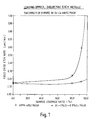
- This graph shows that, for surface coverage ratios larger than 90.0%, the dielectric etch rate through the standard HIPR-6512 photoresist mask is a very steep function of the surface coverage ratio.
- the values indicate that the photoresist loading effect causes an average dielectric etch rate increase of more than 300 % when the surface coverage ratio reaches about 91.8 %.
- the extrapolation of the loading effect curve shows that even larger etch rate increases are projected for larger that 91.8% surface coverage ratios.
- the graph also shows that, for surface coverage ratios larger than 90.0%, the dielectric etch rate through a hard Al/Si/Cu mask is a much smaller function of the surface coverage ratio.
- the values indicate that the hard mask loading effect reduces the average dielectric etch rate increase to less than 12% when the surface coverage ratio reaches about 91.8 %. Since the dielectric etch rate through the hard mask, at 91.8% surface coverage ratio, is not exactly identical to the etch rate without any mask, a slight loading effect remains with the hard mask approach. This loading effect is believed to be due to a gas phase loading effect which could be even more reduced by working at lower pressures and smaller residence times (larger total flow rate) in order to more efficiently remove reaction by-products from the surface and replace them by fresh reactants.
- the extrapolation of the hard mask loading effect curve shows that very reasonable etch rate increases are projected for larger than 91.8% surface coverage ratios.
- the contact patterning mask of advanced devices typically has a surface coverage ratio exceeding 95%, with most of the uncovered surface being occupied by contact pads and scribe lines. The number of such scribe lines drops when fewer number of larger dies can be patterned per wafer. This results in an increase of the surface coverage ratio with die dimensions.
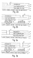
- contact holes 7 are formed by depositing a thin layer of pure aluminum or aluminum alloy 3 over a dielectric to pattern 2.
- the thickness of this layer 2 is minimized in order to improve the pattern transfer accuracy.
- the layer 3 typically has a thickness of about 200nm .
- the dielectric layer 2 is located on a substrate 1 containing active components of the semiconductor device.
- the thickness of this photoresist layer can be small since the thickness of the layer to pattern is also small. This results in better pattern transfer.
- the positive or negative photoresist is soft-baked to low temperatures, typically around 110°C for about 6 minutes in order to evaporate solvents and water.
- the obtained photoactive positive or negative photoresist film 4 is locally exposed by using photomasks and step-and-repeat or projection alignment equipment. This results in local photo-induced chemical reactions in the positive or negative photoresist film located over the aluminum or aluminum alloy film.
- a developer solution is used to locally remove the areas 7 of the positive photoresist at which photo-induced chemical reactions occurred.
- the developer solution is used to remove unexposed regions of negative photoresist.
- the mask pattern is then transferred to the positive photoresist while its reverse image is tansferred when negative photoresist is used.
- the positive or negative photoresist is hard-baked to about 120°C for about 6 minutes in order to stabilize the obtained pattern and make it suitable for underlying dielectric film dry patterning.
- the wafer is transferred to an aluminum or aluminum alloy etcher.
- This etcher may etch the aluminum or aluminum alloy with wet chemicals or may use dry etch chemistries. If a wet etch approach is chosen, a critical dimension loss of about two times the thickness of the aluminum layer results. A dry etch approach results in minimal dimension loss.
- the photoresist pattern is then transferred to the aluminum or aluminum alloy film:
- the wafer is transferred to a photoresist stripper where the photoresist is removed to leave hole 7 ( Figure 3a).
- the removal of the photoresist is known to be very easy at that step and no resist residue results.
- the wafers are transferred to a dielectric dry-etcher to form contact hole 7 ( Figure 4a) .
- the etch is stopped after a certain over-etch time is added to end-point.
- the end-point is more precise because of the reduced loading effect.
- the scribe lines are etched down to the substrate while the contact holes are etched-down to the transistor polysilicon or silicide gates, to substrate or silicide sources and drains as well as to capacitor electrodes and any other electrodes that need to be connected to other devices.
- Figures 2b, 3b, 4c shown the formation of via holes, which are etched down to the first level interconnect patterns.
- the aluminum or aluminum alloy hard mask can be removed or left in place.
- the wafer is then ready for interconnect material deposition.
- the mask can also be made of TiN or a composite TiN/Al layer.
- the use of aluminum or aluminum alloy mask approach over dielectric layers has many advantages.
- the photoresist is much easier to remove over aluminum, after aluminum etch, than over dielectric, after dry dielectric etch.
- the removal of such photoresist does not inquire special equipment and can be done with solvents.
- the interconnect material deposition can be done immediately after completion of the etch step, without interruption and without breaking vacuum.
- the dielectric etch module (which uses an aluminum alloy hard mask) can use a single cluster tool in order to, in-situ and automatically perform the dry etching of the aluminum alloy hard mask, perform the dry stripping of the temporary photoresist, perform the dry etching of contact holes and vias, do the deposition the interconnect material which is normally an aluminum alloy, possibly in combination, with a refractory metal or compound.
- the manufacturing of devices for which the dielectric to be etched does include porous materials, such as spin-on glass, the non-exposure of the porous dielectric media to ambient air prevent moisture re-absorption and via-specific contact resistivity problems.
- This first in-situ and non interrupted cluster tool based integrated processing etch module using hard mask approach constitutes very important improvement over the traditional multi-step, multi-equipment, and multi-operator etch module approach and should be seen as a very efficient way of manufacturing future semiconductor devices.
- the material to be patterned is an aluminum alloy.
- the hard mask left in place is a suitable dielectric, such as a thin oxide layer, a nitride layer, an oxynitride layer, or other common dielectrics used in typical semiconductor processes, and the insulating material deposition is done immediately after the completion of the etch step, without interruption and without breaking vacuum.
- the interconnect etch module which uses an oxide or another dielectric hard mask can use a single cluster tool in order to, in-situ and automatically do the dry etching of the oxide hard mask, do the dry stripping of the temporary photoresist, perform the dry etching of the interconnect lines, do the deposition the insulating material which is normally a silicon oxide layer, doped or not with phosphorus, in combination or not with a silicon nitride or silicon oxinitride layer.
- This second in-situ and non interrupted cluster tool based integrated processing etch module using a hard mask approach constitutes a very important improvement over the traditional multi-step, multi-equipment, and multi-operator etch module approach and is a very efficient way of manufacturing future semiconductor devices.
- the depth-of-focus does not need to be as large and, with the same numerical aperture equipment, better photo capability results, particularly on topography.
- the pattern transfer, from the mask to the resist and from the resist to the hard mask, is improved.
- the hard mask can be made of a different material than aluminum or aluminum alloy; it is nevertheless preferred to not remove the hard mask after contact or via hole patterning and prior to the deposition of the interconnect material in order to make the integrated processing possible.
- the same concept can be applied to the interconnect etch module.
- a hard mask is deposited over the interconnect material to be patterned. If the hard mask is a thin dielectric layer which is suitable to further processing steps, integrated processing can also result.
- This invention describes a way of a hard mask in order to obtain a more reliable dielectric etch module with improved characteristics for large dies (large surface coverage ratio) applications.
Landscapes
- Internal Circuitry In Semiconductor Integrated Circuit Devices (AREA)
- Drying Of Semiconductors (AREA)
Applications Claiming Priority (2)
| Application Number | Priority Date | Filing Date | Title |
|---|---|---|---|
| CA2193905 | 1996-12-24 | ||
| CA002193905A CA2193905A1 (fr) | 1996-12-24 | 1996-12-24 | Traitement integre pour un module grave |
Publications (2)
| Publication Number | Publication Date |
|---|---|
| EP0855737A2 true EP0855737A2 (fr) | 1998-07-29 |
| EP0855737A3 EP0855737A3 (fr) | 1998-12-23 |
Family
ID=4159534
Family Applications (1)
| Application Number | Title | Priority Date | Filing Date |
|---|---|---|---|
| EP97310627A Withdrawn EP0855737A3 (fr) | 1996-12-24 | 1997-12-24 | Procédé de gravure utilisant un masque dur |
Country Status (3)
| Country | Link |
|---|---|
| US (1) | US6074946A (fr) |
| EP (1) | EP0855737A3 (fr) |
| CA (1) | CA2193905A1 (fr) |
Cited By (3)
| Publication number | Priority date | Publication date | Assignee | Title |
|---|---|---|---|---|
| EP1137058A1 (fr) * | 2000-03-23 | 2001-09-26 | Motorola, Inc. | Méthode pour structurer des couches de dispositifs semiconducteurs |
| EP1286388A1 (fr) * | 2001-08-23 | 2003-02-26 | Texas Instruments Incorporated | Masque dur en aluminium pour gravure d'un diélectrique |
| EP1180794A3 (fr) * | 2000-08-18 | 2004-08-25 | Infineon Technologies AG | Contrôle du processus pour la fabrication de contacts métal/métal |
Families Citing this family (16)
| Publication number | Priority date | Publication date | Assignee | Title |
|---|---|---|---|---|
| JP3938253B2 (ja) | 1997-12-26 | 2007-06-27 | 日本板硝子株式会社 | 樹脂正立等倍レンズアレイおよびその製造方法 |
| US6399446B1 (en) * | 1999-10-29 | 2002-06-04 | Advanced Micro Devices, Inc. | Process for fabricating high density memory cells using a metallic hard mask |
| US6342164B1 (en) * | 2000-07-31 | 2002-01-29 | Motorola, Inc. | Pinhole-free dielectric films |
| DE10237249B4 (de) * | 2002-08-14 | 2014-12-18 | Excelitas Technologies Singapore Pte Ltd | Verfahren zum selektiven Abtragen von Material aus der Oberfläche eines Substrats |
| US7301752B2 (en) * | 2004-06-04 | 2007-11-27 | International Business Machines Corporation | Formation of metal-insulator-metal capacitor simultaneously with aluminum metal wiring level using a hardmask |
| JP2009169993A (ja) * | 2008-01-10 | 2009-07-30 | Fuji Electric Device Technology Co Ltd | パターンドメディア型磁気記録媒体の製造方法 |
| US7803720B2 (en) * | 2008-01-25 | 2010-09-28 | Kabushiki Kaisha Toshiba | Coating process and equipment for reduced resist consumption |
| WO2010127941A1 (fr) | 2009-05-07 | 2010-11-11 | Basf Se | Compositions de décapage de résine photosensible et procédés de fabrication de dispositifs électriques |
| WO2010127942A1 (fr) | 2009-05-07 | 2010-11-11 | Basf Se | Compositions de décapage de résine photosensible et procédés de fabrication de dispositifs électriques |
| JP5836932B2 (ja) | 2009-05-07 | 2015-12-24 | ビーエーエスエフ ソシエタス・ヨーロピアBasf Se | レジストストリッピング組成物及び電気装置を製造するための方法 |
| US8399359B2 (en) | 2011-06-01 | 2013-03-19 | United Microelectronics Corp. | Manufacturing method for dual damascene structure |
| US8735295B2 (en) | 2012-06-19 | 2014-05-27 | United Microelectronics Corp. | Method of manufacturing dual damascene structure |
| US8647991B1 (en) | 2012-07-30 | 2014-02-11 | United Microelectronics Corp. | Method for forming dual damascene opening |
| US8921226B2 (en) | 2013-01-14 | 2014-12-30 | United Microelectronics Corp. | Method of forming semiconductor structure having contact plug |
| US8962490B1 (en) | 2013-10-08 | 2015-02-24 | United Microelectronics Corp. | Method for fabricating semiconductor device |
| JP7027200B2 (ja) * | 2018-03-09 | 2022-03-01 | キオクシア株式会社 | レプリカテンプレートの製造方法、及び半導体装置の製造方法 |
Family Cites Families (6)
| Publication number | Priority date | Publication date | Assignee | Title |
|---|---|---|---|---|
| JPS5978585A (ja) * | 1982-10-27 | 1984-05-07 | Hitachi Ltd | ジヨセフソン集積回路 |
| DE3381302D1 (de) * | 1982-12-16 | 1990-04-12 | Fujitsu Ltd | Herstellung eines halbleiterbauelementes mittels molekularstrahlepitaxie. |
| JPH03156927A (ja) * | 1989-10-24 | 1991-07-04 | Hewlett Packard Co <Hp> | アルミ・メタライゼーションのパターン形成方法 |
| JPH05326719A (ja) * | 1992-05-27 | 1993-12-10 | Oki Electric Ind Co Ltd | 半導体素子の製造方法 |
| US5547896A (en) * | 1995-02-13 | 1996-08-20 | Harris Corporation | Direct etch for thin film resistor using a hard mask |
| WO1996027899A1 (fr) * | 1995-03-08 | 1996-09-12 | International Business Machines Corporation | Procede d'attaque au plasma d'une structure en oxyde/silicium polycristallin siliciure |
-
1996
- 1996-12-24 CA CA002193905A patent/CA2193905A1/fr not_active Abandoned
-
1997
- 1997-02-04 US US08/794,441 patent/US6074946A/en not_active Expired - Lifetime
- 1997-12-24 EP EP97310627A patent/EP0855737A3/fr not_active Withdrawn
Cited By (4)
| Publication number | Priority date | Publication date | Assignee | Title |
|---|---|---|---|---|
| EP1137058A1 (fr) * | 2000-03-23 | 2001-09-26 | Motorola, Inc. | Méthode pour structurer des couches de dispositifs semiconducteurs |
| EP1180794A3 (fr) * | 2000-08-18 | 2004-08-25 | Infineon Technologies AG | Contrôle du processus pour la fabrication de contacts métal/métal |
| EP1286388A1 (fr) * | 2001-08-23 | 2003-02-26 | Texas Instruments Incorporated | Masque dur en aluminium pour gravure d'un diélectrique |
| US6620727B2 (en) | 2001-08-23 | 2003-09-16 | Texas Instruments Incorporated | Aluminum hardmask for dielectric etch |
Also Published As
| Publication number | Publication date |
|---|---|
| US6074946A (en) | 2000-06-13 |
| CA2193905A1 (fr) | 1998-06-24 |
| EP0855737A3 (fr) | 1998-12-23 |
Similar Documents
| Publication | Publication Date | Title |
|---|---|---|
| US6074946A (en) | Integrated processing for an etch module using a hard mask technique | |
| US5346586A (en) | Method for selectively etching polysilicon to gate oxide using an insitu ozone photoresist strip | |
| US5747380A (en) | Robust end-point detection for contact and via etching | |
| US5895740A (en) | Method of forming contact holes of reduced dimensions by using in-situ formed polymeric sidewall spacers | |
| US6291137B1 (en) | Sidewall formation for sidewall patterning of sub 100 nm structures | |
| US6444557B1 (en) | Method of forming a damascene structure using a sacrificial conductive layer | |
| US5013398A (en) | Anisotropic etch method for a sandwich structure | |
| US6559049B2 (en) | All dual damascene oxide etch process steps in one confined plasma chamber | |
| JP5134363B2 (ja) | プラズマ加工システムによる基板エッチング法 | |
| US5792672A (en) | Photoresist strip method | |
| US5925577A (en) | Method for forming via contact hole in a semiconductor device | |
| US5851302A (en) | Method for dry etching sidewall polymer | |
| US8143138B2 (en) | Method for fabricating interconnect structures for semiconductor devices | |
| EP0473344B1 (fr) | Procédé pour l'attaque d'une structure bi-couche conducteur | |
| US5332653A (en) | Process for forming a conductive region without photoresist-related reflective notching damage | |
| US6420099B1 (en) | Tungsten hard mask for dry etching aluminum-containing layers | |
| US6027959A (en) | Methods for in-situ removal of an anti-reflective coating during a nitride resistor protect etching process | |
| JP2891952B2 (ja) | 半導体装置の製造方法 | |
| KR20000057897A (ko) | 지정된 기판 상에 놓여져 있는 패턴화된 마스크 표면 위로조립 구조물을 증착하기 위한 방법 | |
| EP0731501A1 (fr) | Procédé d'attaque par plasma d'une structure oxide/polycide | |
| US6057230A (en) | Dry etching procedure and recipe for patterning of thin film copper layers | |
| WO1996027899A1 (fr) | Procede d'attaque au plasma d'une structure en oxyde/silicium polycristallin siliciure | |
| US6171940B1 (en) | Method for fabricating semiconductor devices having small dimension gate structures | |
| US4980301A (en) | Method for reducing mobile ion contamination in semiconductor integrated circuits | |
| EP1320128A1 (fr) | Méthode de fabrication de structures d'interconnexion |
Legal Events
| Date | Code | Title | Description |
|---|---|---|---|
| PUAI | Public reference made under article 153(3) epc to a published international application that has entered the european phase |
Free format text: ORIGINAL CODE: 0009012 |
|
| AK | Designated contracting states |
Kind code of ref document: A2 Designated state(s): DE FR |
|
| AX | Request for extension of the european patent |
Free format text: AL;LT;LV;MK;RO;SI |
|
| PUAL | Search report despatched |
Free format text: ORIGINAL CODE: 0009013 |
|
| AK | Designated contracting states |
Kind code of ref document: A3 Designated state(s): AT BE CH DE DK ES FI FR GB GR IE IT LI LU MC NL PT SE |
|
| AX | Request for extension of the european patent |
Free format text: AL;LT;LV;MK;RO;SI |
|
| 17P | Request for examination filed |
Effective date: 19990616 |
|
| AKX | Designation fees paid |
Free format text: DE FR |
|
| RAP1 | Party data changed (applicant data changed or rights of an application transferred) |
Owner name: ZARLINK SEMICONDUCTOR INC. |
|
| RAP1 | Party data changed (applicant data changed or rights of an application transferred) |
Owner name: DALSA SEMICONDUCTOR INC. |
|
| 17Q | First examination report despatched |
Effective date: 20040116 |
|
| 17Q | First examination report despatched |
Effective date: 20040116 |
|
| STAA | Information on the status of an ep patent application or granted ep patent |
Free format text: STATUS: THE APPLICATION IS DEEMED TO BE WITHDRAWN |
|
| 18D | Application deemed to be withdrawn |
Effective date: 20070920 |