EP0855797A2 - Condensatuer à jonction semiconducteur pour la mise en formes d'ondes avec compensation - Google Patents
Condensatuer à jonction semiconducteur pour la mise en formes d'ondes avec compensation Download PDFInfo
- Publication number
- EP0855797A2 EP0855797A2 EP98300289A EP98300289A EP0855797A2 EP 0855797 A2 EP0855797 A2 EP 0855797A2 EP 98300289 A EP98300289 A EP 98300289A EP 98300289 A EP98300289 A EP 98300289A EP 0855797 A2 EP0855797 A2 EP 0855797A2
- Authority
- EP
- European Patent Office
- Prior art keywords
- diode
- linearizing
- wave
- junction capacitance
- circuit
- Prior art date
- Legal status (The legal status is an assumption and is not a legal conclusion. Google has not performed a legal analysis and makes no representation as to the accuracy of the status listed.)
- Withdrawn
Links
Images

Classifications
-
- H—ELECTRICITY
- H03—ELECTRONIC CIRCUITRY
- H03K—PULSE TECHNIQUE
- H03K5/00—Manipulating of pulses not covered by one of the other main groups of this subclass
- H03K5/01—Shaping pulses
-
- H—ELECTRICITY
- H03—ELECTRONIC CIRCUITRY
- H03K—PULSE TECHNIQUE
- H03K5/00—Manipulating of pulses not covered by one of the other main groups of this subclass
- H03K5/01—Shaping pulses
- H03K5/04—Shaping pulses by increasing duration; by decreasing duration
- H03K5/06—Shaping pulses by increasing duration; by decreasing duration by the use of delay lines or other analogue delay elements
Definitions
- the present invention relates generally to wave-shaping circuits, and more specifically to wave-shaping circuits for simple integrated circuit (IC) processes, such as MOS (Metal Oxide Silicon) and MIM (Metal Insulated Metal), that do not have area efficient dielectric capacitors.
- IC integrated circuit
- MOS Metal Oxide Silicon
- MIM Metal Insulated Metal
- the high frequency content of an electrical waveform is related to the time-varying nature of the waveform.
- fast changes in waveform amplitude are indicative of increased high frequency content.
- a square wave representation for example, becomes more accurate as the number of high frequency harmonics included in the representation is increased.
- An infinite number of harmonics would be required to perfectly represent a square wave.
- Modern digital devices typically utilize square waves and rectangular waveforms, which have similar characteristics.
- Increased high frequency content of an electrical waveform can cause problems in electrical circuits and systems. While higher frequency content of an electrical waveform may do no harm in the circuit utilizing the waveform if rise and fall times are faster than required, it is well known in the art that high frequency signals emit electromagnetic radiation that can couple into adjoining circuits and equipments causing problems such as mis-triggering. For example, a tunable radio receiver in proximity to an operating computer can easily detect the existence of many frequencies utilized in the computer and harmonics of those frequencies. It is thus possible and in fact commonplace for digital devices to interfere with wireless communications.
- a number of approaches may be used to reduce the magnitude of this problem. Shielding of higher frequency circuitry is common, wherein metallic barriers to electromagnetic radiation are erected in an attempt to contain the radiation in a restricted volume. Electrical filtering is commonplace, seeking to reduce the high frequency content on signal paths entering or leaving an area containing circuitry or equipment which contain high frequency signals. Shielding and filtering of an area which will be adversely affected by coupled electromagnetic radiation is also commonplace. At a higher level, government agencies often put quantitative restrictions on the level of high frequencies which may be radiated or conducted from a given equipment. All of the above solutions, however, are only successful to varying degrees and add size and cost. It is well known in the art that it is better to not generate high frequencies unless they are required.
- the higher frequency harmonics can be greatly reduced.
- the higher frequency harmonic content can be minimized if the fast amplitude changes which occur at the edges of a square wave are replaced by amplitude changes which exhibit a constant time rate of change, and if the remaining corners are rounded off. It is clear that digital circuits require rectangular waveforms which change sufficiently fast so as to obtain the required operation, but it is not normally required that these waveforms be excessively faster than this. It is therefore understood in the art that the rise and fall times generated in digital circuitry may be increased and the corners may be rounded as long as one remains within the bounds of good engineering practice.
- Wave-shaping may be applied at any physical level of electrical circuitry, such as with discrete components or within integrated circuits.
- the constant slew rate referred to above is achieved in integrated circuits by charging an on-chip capacitor C1 with a constant current source I as shown in Figure 2 .
- I CdV/dT
- the remaining wave-shaping step is achieved by integrating the constant slew rate onto a second capacitor C2.
- CMOS Complementary Metal Oxide Silicon
- MOS Metal Oxide Silicon
- a method and structure for wave-shaping of digital waveforms of integrated circuit processes that do not have area efficient dielectric capacitors is disclosed.
- the dielectric capacitors of the prior art are replaced with a first, linearizing diode and a second diode of a wave-shaping circuit, each diode having a junction capacitance that varies with voltage applied across the diode.
- the first, linearizing diode is supplied with a constant current from a constant current source.
- a current inversely proportional to the junction capacitance of the first, linearizing diode is produced by a transconductance amplifier supplied with a linear voltage at a node defined as the connection between the constant current source and the first linearizing diode.
- the current at the node is supplied to the second diode to produce an output voltage of the wave-shaping circuit that is linear with respect to time.
- the output voltage of the wave-shaping circuit has a constant slew rate that compensates for any process and temperature variations in the first, linearizing diode and the second diode.
- the constant current supplied to the linearizing diode may be varied to produce desired controlled corner rounding.
- Wave-shaping of rectangular digital waveforms is often required to reduce the amount of high frequency content in these signals since electromagnetic radiation and conduction of high frequency energy is known to produce interference to other circuitry and equipment, often with disastrous results.
- a number of wave-shaping techniques are known in the art, but in the area of inexpensive bipolar IC processes there still exists a need for a simple wave-shaping technique which is compatible with the required IC production processes.
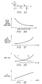
- wave-shaping schematic (A) which utilizes the junction capacitance of diodes D1 and D2 to replace the capacitors C2 and C1 in the prior art technique of Figure 2.
- Waveform B illustrates the basic manner in which diode junction capacitance varies with voltage applied across the diode
- waveform C illustrates the manner in which Vb would vary versus time if diode D2 were a fixed capacitor, as in the prior art.
- Waveform D shows how the voltage Va and the current Ib, which is inversely proportional to the junction capacitance of D2, are related. Since the junction capacitance of D1 varies in the same manner as D2 with applied voltage, the overall output Vb will be linear with respect to time (waveform E).
- a natural consequence and a novel feature of the present invention is that output Vb automatically compensates for process and temperature variations in the characteristics of the diodes D1 and D2.
- the linear current is transformed by the junction capacitor of diode D2 and the transconductance amplifier to have a transfer function characteristic that is inverse to that of diode D1.
- This transfer function sets the ratio of D1 charging current to integrating capacitance to a constant, which produces the desired effect of a fixed slew rate output voltage Vb that is independent of process and temperature variations. For example, for a given la and with a change in junction capacitance of D2 due to temperature or process variations, voltage Va will change value.
- This changed value of Va will produce a change in current Ib which, when applied to charge the junction capacitance of D1 (the capacitance of D1 changes in a manner identical to D2), produces a compensating effect that tends to force Vb to remain constant.
- the circuit of the present invention will also respond to modifications in the shape of la, and such modifications could be designed by those proficient in the art to produce controlled corner rounding of output Vb.
- the present invention teaches a practical method whereby a wave-shaping function may be implemented within the process requirements used for certain classes of bipolar integrated circuits. Two diodes are utilized, and voltage and temperature coefficients of the diodes are linearized in the present invention. The constant current input to the circuit of the present invention may be varied to produce controlled corner rounding by one skilled in the art.
- the present invention overcomes prior art limitations to allow wave-shaping functions to be integrated in simple bipolar processes.
Landscapes
- Physics & Mathematics (AREA)
- Nonlinear Science (AREA)
- Semiconductor Integrated Circuits (AREA)
- Filters And Equalizers (AREA)
- Amplifiers (AREA)
- Bipolar Integrated Circuits (AREA)
Applications Claiming Priority (2)
| Application Number | Priority Date | Filing Date | Title |
|---|---|---|---|
| US787976 | 1997-01-23 | ||
| US08/787,976 US5952858A (en) | 1997-01-23 | 1997-01-23 | Junction capacitor compensation for wave shaping |
Publications (2)
| Publication Number | Publication Date |
|---|---|
| EP0855797A2 true EP0855797A2 (fr) | 1998-07-29 |
| EP0855797A3 EP0855797A3 (fr) | 1999-07-21 |
Family
ID=25143070
Family Applications (1)
| Application Number | Title | Priority Date | Filing Date |
|---|---|---|---|
| EP98300289A Withdrawn EP0855797A3 (fr) | 1997-01-23 | 1998-01-16 | Condensatuer à jonction semiconducteur pour la mise en formes d'ondes avec compensation |
Country Status (3)
| Country | Link |
|---|---|
| US (1) | US5952858A (fr) |
| EP (1) | EP0855797A3 (fr) |
| JP (1) | JPH10294632A (fr) |
Families Citing this family (1)
| Publication number | Priority date | Publication date | Assignee | Title |
|---|---|---|---|---|
| JP5200053B2 (ja) * | 2010-04-26 | 2013-05-15 | 幸治 越智 | パルス発生器、パルス整形方法 |
Family Cites Families (9)
| Publication number | Priority date | Publication date | Assignee | Title |
|---|---|---|---|---|
| US3676697A (en) * | 1970-10-23 | 1972-07-11 | Sperry Rand Corp | Sweep and gate generator |
| US3731232A (en) * | 1971-07-13 | 1973-05-01 | Hekimian Laboratories Inc | Phantastron circuit employing operational amplifier |
| JPS56129423A (en) * | 1980-03-14 | 1981-10-09 | Sony Corp | Triangle wave generating circuit |
| GB8414313D0 (en) * | 1984-06-05 | 1984-07-11 | Motorola Inc | Timebase circuit |
| JPH0659024B2 (ja) * | 1985-12-23 | 1994-08-03 | 日本電気株式会社 | 時定数回路 |
| SU1667226A2 (ru) * | 1988-08-23 | 1991-07-30 | Предприятие П/Я Г-4335 | Формирователь пр моугольных импульсов |
| JP2686036B2 (ja) * | 1993-07-09 | 1997-12-08 | 浜松ホトニクス株式会社 | アバランシェフォトダイオードのバイアス回路 |
| US5502410A (en) * | 1994-03-14 | 1996-03-26 | Motorola, Inc. | Circuit for providing a voltage ramp signal |
| US5642067A (en) * | 1995-07-26 | 1997-06-24 | Grace; James W. | Variable slew rate pulse generator |
-
1997
- 1997-01-23 US US08/787,976 patent/US5952858A/en not_active Expired - Lifetime
-
1998
- 1998-01-16 EP EP98300289A patent/EP0855797A3/fr not_active Withdrawn
- 1998-01-23 JP JP10011637A patent/JPH10294632A/ja active Pending
Also Published As
| Publication number | Publication date |
|---|---|
| JPH10294632A (ja) | 1998-11-04 |
| EP0855797A3 (fr) | 1999-07-21 |
| US5952858A (en) | 1999-09-14 |
Similar Documents
| Publication | Publication Date | Title |
|---|---|---|
| US5399996A (en) | Circuit and method for minimizing electromagnetic emissions | |
| KR100772747B1 (ko) | 집적회로제조를위한넓은주파수범위및낮은잡음의전압제어발진기 | |
| US6225859B1 (en) | Integrated low-pass filter | |
| EP0435472A2 (fr) | Filtre actif | |
| EP0767532A1 (fr) | Circuit d'oscillation et procédé d'oscillation | |
| US20050001691A1 (en) | Wideband variable frequency voltage controlled oscillator | |
| US5952858A (en) | Junction capacitor compensation for wave shaping | |
| EP0418899B1 (fr) | Circuit amplificateur | |
| KR100464446B1 (ko) | 임피던스 스케일링에 의한 주파수 응답 제어 장치 | |
| RU2273088C1 (ru) | Генератор хаотических колебаний | |
| US5414354A (en) | Apparatus and method for generating a substantially rectangular output signal | |
| US3319079A (en) | Active phase shift compensation network | |
| CN118740129A (zh) | 一种实现谐波补偿的射频开关电路、芯片及电子设备 | |
| US6208191B1 (en) | Positive and negative voltage clamp for a wireless communication input circuit | |
| EP1378055B1 (fr) | Oscillateur electrique servant a controler la forme d'onde et l' amplitude d'un signal | |
| US6392454B1 (en) | Shunt regulated push-pull circuit having wide frequency range | |
| Mei | From Kirchoff to Lorentz modifying-circuit theory for microwave and mm-wave structures | |
| US3421020A (en) | Step voltage generator | |
| EP0663723B1 (fr) | Circuit filtrant | |
| US4146846A (en) | Amplifier having a high frequency boost network | |
| KR100226594B1 (ko) | 전자회로 및 이를 이용한 필터장치 | |
| US3399277A (en) | Signal translating circuit | |
| EP1430598A2 (fr) | Polarisation dynamique d'emetteur | |
| US5973539A (en) | Mixer circuit for mixing two signals having mutually different frequencies | |
| US5767526A (en) | Bipolar resonant tunneling transistor frequency multiplier |
Legal Events
| Date | Code | Title | Description |
|---|---|---|---|
| PUAI | Public reference made under article 153(3) epc to a published international application that has entered the european phase |
Free format text: ORIGINAL CODE: 0009012 |
|
| AK | Designated contracting states |
Kind code of ref document: A2 Designated state(s): DE FR GB IT |
|
| AX | Request for extension of the european patent |
Free format text: AL;LT;LV;MK;RO;SI |
|
| RIN1 | Information on inventor provided before grant (corrected) |
Inventor name: NOTARO, JOSEPH Inventor name: EDWARDS, WILLIAM ERNEST |
|
| RAP3 | Party data changed (applicant data changed or rights of an application transferred) |
Owner name: STMICROELECTRONICS, INC. |
|
| PUAL | Search report despatched |
Free format text: ORIGINAL CODE: 0009013 |
|
| AK | Designated contracting states |
Kind code of ref document: A3 Designated state(s): AT BE CH DE DK ES FI FR GB GR IE IT LI LU MC NL PT SE |
|
| AX | Request for extension of the european patent |
Free format text: AL;LT;LV;MK;RO;SI |
|
| RIC1 | Information provided on ipc code assigned before grant |
Free format text: 6H 03K 5/02 A |
|
| 17P | Request for examination filed |
Effective date: 20000114 |
|
| AKX | Designation fees paid |
Free format text: DE FR GB IT |
|
| 17Q | First examination report despatched |
Effective date: 20020424 |
|
| STAA | Information on the status of an ep patent application or granted ep patent |
Free format text: STATUS: THE APPLICATION IS DEEMED TO BE WITHDRAWN |
|
| 18D | Application deemed to be withdrawn |
Effective date: 20040824 |