EP0856201B1 - Detecteur de rayonnement a heterostructure de semi-conducteur, pourvu de deux zones de sensibilite spectrales - Google Patents
Detecteur de rayonnement a heterostructure de semi-conducteur, pourvu de deux zones de sensibilite spectrales Download PDFInfo
- Publication number
- EP0856201B1 EP0856201B1 EP96945510A EP96945510A EP0856201B1 EP 0856201 B1 EP0856201 B1 EP 0856201B1 EP 96945510 A EP96945510 A EP 96945510A EP 96945510 A EP96945510 A EP 96945510A EP 0856201 B1 EP0856201 B1 EP 0856201B1
- Authority
- EP
- European Patent Office
- Prior art keywords
- quantum well
- hetero structure
- photo
- radiation detector
- band
- Prior art date
- Legal status (The legal status is an assumption and is not a legal conclusion. Google has not performed a legal analysis and makes no representation as to the accuracy of the status listed.)
- Expired - Lifetime
Links
Images
Classifications
-
- H—ELECTRICITY
- H10—SEMICONDUCTOR DEVICES; ELECTRIC SOLID-STATE DEVICES NOT OTHERWISE PROVIDED FOR
- H10F—INORGANIC SEMICONDUCTOR DEVICES SENSITIVE TO INFRARED RADIATION, LIGHT, ELECTROMAGNETIC RADIATION OF SHORTER WAVELENGTH OR CORPUSCULAR RADIATION
- H10F77/00—Constructional details of devices covered by this subclass
- H10F77/10—Semiconductor bodies
- H10F77/14—Shape of semiconductor bodies; Shapes, relative sizes or dispositions of semiconductor regions within semiconductor bodies
-
- H—ELECTRICITY
- H10—SEMICONDUCTOR DEVICES; ELECTRIC SOLID-STATE DEVICES NOT OTHERWISE PROVIDED FOR
- H10F—INORGANIC SEMICONDUCTOR DEVICES SENSITIVE TO INFRARED RADIATION, LIGHT, ELECTROMAGNETIC RADIATION OF SHORTER WAVELENGTH OR CORPUSCULAR RADIATION
- H10F30/00—Individual radiation-sensitive semiconductor devices in which radiation controls the flow of current through the devices, e.g. photodetectors
- H10F30/20—Individual radiation-sensitive semiconductor devices in which radiation controls the flow of current through the devices, e.g. photodetectors the devices having potential barriers, e.g. phototransistors
- H10F30/21—Individual radiation-sensitive semiconductor devices in which radiation controls the flow of current through the devices, e.g. photodetectors the devices having potential barriers, e.g. phototransistors the devices being sensitive to infrared, visible or ultraviolet radiation
- H10F30/22—Individual radiation-sensitive semiconductor devices in which radiation controls the flow of current through the devices, e.g. photodetectors the devices having potential barriers, e.g. phototransistors the devices being sensitive to infrared, visible or ultraviolet radiation the devices having only one potential barrier, e.g. photodiodes
- H10F30/223—Individual radiation-sensitive semiconductor devices in which radiation controls the flow of current through the devices, e.g. photodetectors the devices having potential barriers, e.g. phototransistors the devices being sensitive to infrared, visible or ultraviolet radiation the devices having only one potential barrier, e.g. photodiodes the potential barrier being a PIN barrier
Definitions
- the invention relates to a semiconductor heterostructure radiation detector, of the two spectral sensitivity ranges having.
- the two spectral Sensitivity areas result from contiguous Semiconductor layer areas in which photons absorbable with different energies are.
- the photons rain in the semiconductor layer areas existing charge carriers so optically so that depending on an external electrical voltage, the via electrodes attached to the semiconductor layer structure are provided, a photocurrent can be generated.
- photodiodes known with conventional p-i-n junctions also so-called quantum well inter-band photodetectors (QWIP), whose spectral sensitivity properties through appropriate choice of material layer systems, Layer thickness parameters and the choice of n or p-doping can be set.
- QWIP quantum well inter-band photodetectors
- conventional Photodiodes have spectral sensitivities in the visible up to the near infrared spectral range. ever depending on the choice of material, you can also use wavelengths in Detect ⁇ m range.
- the so-called quantum well intersubband photodetectors have spectral sensitivity ranges per se in the longer-wave spectral range, preferably in the range between 3 and 20 ⁇ m range, which is determined by the choice of material and layer thickness parameters let set.
- quantum well structures are used, which are by dimensioning that for the quantum well structure characteristic barrier height or band gap as well Differentiate pot width or layer thickness.
- QWIP structures are doped by an additional one Contact layer separated from each other. The on this Physical separation that can be achieved in this way does Advantage that the two QWIP structures are separate be optimized for their respective working wavelength can, but this arrangement has the disadvantage that through the separation for the power supply at least an additional electrode is required.
- the invention is based on the object of a semiconductor heterostructure radiation detector which has two adjoining semiconductor layer regions which are sensitive in different spectral regions and in which photons with different energies can be absorbed in each case and which optically excite charge carriers present in the semiconductor layer regions such that a photocurrent in the
- the respective semiconductor layer areas can be generated in dependence on an external electrical voltage applied via electrodes provided on the semiconductor heterostructure in such a way that the spectral sensitivity areas in the semiconductor layer structures can be set separately from one another without lasting influence on the overall noise behavior of the two-color detector.
- the noise behavior of the two-color detector is to be dominated by the noise of the active individual detector.
- the invention is based on the finding of a semiconductor heterostructure radiation detector according to the generic term of claim 1 so that the two adjoining each other in their spectral Sensitivity areas distinguishing semiconductor layer areas from the combination of a photodiode and a quantum well inter-subband photodetector.
- the combination of a photodiode according to the invention with a QWIP structure it is different from the previous ones Approaches for the realization of electrically tunable Two-color detectors managed to reduce the noise behavior of the two-color detector according to the invention by the noise of the active individual detector is determined.
- the structure is preferably different Individual detectors applied to a base substrate in such a way so that with the means of epitaxial deposition processes, preferably the molecular beam epitaxy method, the layer sequence of a p-i-n photodiode a base substrate is deposited over which in the immediate Sequence the layer sequence of a quantum well inter-subband photodetector is applied.
- the layer sequence of a p-i-n photodiode a base substrate is deposited over which in the immediate Sequence the layer sequence of a quantum well inter-subband photodetector is applied.
- at least two electrodes are provided, one of which the one with the opposite of the QWIP structure Contact layer of the photodiode and the other electrode with the top cover of the QWIP structure becomes.
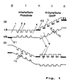
- FIG. 1 The band diagrams of an advantageous embodiment of the two-color detector according to the invention are shown in FIG. 1 in sub-figures a and b.
- the lines lying opposite each other in the partial figures correspond to the valence (VB) and the conduction band (LB).
- the layer sequence is chosen such that it starts with the left edge on a base substrate layer, the a p-doped GaAs layer (1) is applied from GaAs which is also the p-area of the p-i-n photodiode represents. For the rest, all the other layer sequences are with the help of molecular beam epitaxy applied.
- the characteristic of a photodiode intrinsic (i) area exhibits a multitude, thinner, alternating InGaAs layers (2) in succession with GaAs layers (3) on. The layers correspond with this smaller band gaps in the areas of the InGaAs layers, whereas the layer areas of larger band gaps Contain GaAs.
- the i-layer formed in this way serves especially the expansion of the sensitivity range towards wavelengths for which the GaAs substrate is transparent.
- an n-doped GaAs layer (4) deposited On the so-called in the i-area Multiquantum well structure is an n-doped GaAs layer (4) deposited. It also poses represents the n region of the p-i-n photodiode.
- a quantum well inter-subband structure applied, the layer sequences of AlGaAs (5) and GaAs (6). Correspond to areas with a larger band gap the AlGaAs layers, whereas the ones in between Areas with a smaller band gap each made of n-doped GaAs exist.
- the Quantum Intersubband structure final top layer is an n-doped GaAs layer used.
- the quantum well structure is dimensioned such that that the charge carriers located in the potential wells L assume quantized states and that the barrier height, due to the large band gap in the AlGaAs layers are determined, tunneling of the charge carriers exclude from one to the other potential well.
- the combination of a photodiode and a QWIP structure is according to the embodiment of the 1 as indicated there with the electrodes E1, E2 and E3 provided.
- the electrode E2 which is preferably on the n range the photodiode is applied as floating Electrode executed.
- An external voltage is applied via the electrodes E1 and E2 created, which in case a) is chosen such that the Photodiode is in the forward direction.
- the QWIP structure is characterized by tensions due to the external, existing electrical Field bent so that due to optical excitation the electrons in the lower interbands are excited into upper, not shown states, which are near or above the edge of the charge band.
- Such optical carriers can be used for optical excitation Part also in the continuum, i.e. about the conduction band edge energy, be lifted so that they are due to the outer electrical field are immediately pulled off to the side and can contribute to the photocurrent in this way.
- the operating state of the two-color detector according to Figure 1a represents the case where the spectral sensitivity range the QWIP structure predominates, which makes the forming photocurrent solely from charge carriers composed due to intersubband absorption processes originate.
- Two-color detector is that Noise behavior of the overall detector from the part of the detector is determined in which the respective photocurrent is generated. This is particularly because the reverse polarity of the photodiode is extremely high Dark resistance, against which the differential Internal resistance of the QWIP structure can be neglected can.
- the differential internal resistance of the Photodiode which is polarized in the forward direction, one such a small value that the noise component from this Detector area compared to the noise component of the active operated QWIP structure through suitable choice of materials can be neglected.
- the two-color detector is as specified in the Example according to FIG. 1 in this way to two wavelengths optimize so that longer-wave radiation components from the QWIP structure and shorter wavelength components from the p-i-n photodiode be absorbed.
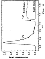
- FIG. 2 shows a diagram from which the spectral Sensitivity behavior depending on the photon energy of the two-color detector shown in FIG two different tension ratios is.
- the spectral sensitivity is in amperes per irradiated Photon power in watts along the ordinate shown.
- the photon energies are on the abscissa applied.
- the spectral sensitivity with respect to the photodiode is in the QWIP structure 0.5 A / W at a photon energy from 153 meV.
- a bias voltage of 1 volt in the reverse direction adjusted with respect to the photodiode it follows spectral sensitivity in the area of the photodiode of 0.18 A / W with a photon energy of 1.47 eV.
- Measurement data correspond to the detector sensitivities of known individual detectors, so that can be shown that the combination of a radiation detector consisting of a photodiode and a quantum well intersubband photodetector similar detection properties has, as is the case with individual detectors in Unique is the case.
- Two-color detectors In addition to the specific embodiment of the Two-color detectors according to the invention are also others Material combinations or doping options conceivable. So n-i-p photodiodes can also be used and with a corresponding p-doped quantum well structure be combined. Inverted layer orders are also conceivable, where first the QWIP structure and only then the layers of the photodiode on the substrate be deposited. Additional configurations result for example when using a p-doped Quantumwell inter-subband photodetectors, i.e. a QWIP structure with p-doped quantum well layers and one p-type contact.
- a multi-layer sequence consisting of GaSb / AlGaSb are deposited via either as InAs photodiode layer or a superlattice consisting of GaSb-InAs or existing AlGaSb / InGaSb are deposited can.
- the radiation in the spectral sensitivity range of the quantum well intersubband photodetector is at an angle bends to the direction of incidence.
- the two-color detectors according to the invention can be operated in individual operation as well as in an array arrangement.
- Typical lateral dimensions of a single detector are (10-1000 ⁇ m) 2 with typical total layer thicknesses of a few ⁇ m.
- Such two-color detectors are used in particular in so-called focal plane array camera systems which are used, for example, for thermography.
Landscapes
- Light Receiving Elements (AREA)
Claims (17)
- Détecteur de rayonnement à hétéro structure de semi-conducteur comprenant deux régions contiguës à couches semi-conductrices sensibles au-dedans de gammes spectrales différentes, dans lesquelles des photons aux niveaux d'énergie différents respectifs peuvent être absorbé, qui excitent, de façon optique, des porteurs de charge présents dans les régions à couches semi-conducteurs d'une telle manière qu'un courant photoélectrique peut être engendré dans les régions respectives à couches semi-conducteurs en fonction d'une tension électrique extérieure appliquée via des électrodes disposées sur la hétéro structure de semi-conducteur,
caractérisé en ce que le détecteur de rayonnement à hétéro structure de semi-conducteur présente une structure p-i-n-i-n ou une structure n-i-p-i-p, en ce qu'une région de la couche semi-conducteur est une photodiode p-i-n, pendant que l'autre région est un détecteur photoélectrique à puits quantiques à intersous-bandes. - Détecteur de rayonnement à hétéro structure de semi-conducteur selon la revendication 1,
caractérisé en ce que le détecteur photoélectrique à puits quantiques à intersous-bandes est du type de conduction en n, et en ce que la photodiode présente une région dopée en n, contiguës au détecteur photoélectrique à puits quantiques à intersous-bandes,
et en ce qu'une électrode est disposée sur la région dopée en p de la photodiode, pendant qu'une deuxième électrode est disposée sur le détecteur photoélectrique à puits quantiques à intersous-bandes pour l'application d'une tension extérieure. - Détecteur de rayonnement à hétéro structure de semi-conducteur selon la revendication 1,
caractérisé en ce que le détecteur photoélectrique à puits quantiques à intersous-bandes est du type de conduction p, et que la photodiode présente une région dopée en p, contiguë ledit détecteur photoélectrique à puits quantiques à intersous-bandes,
et en ce qu'une électrode est montée sur la région dopée en p de ladite photodiode, pendant qu'une deuxième électrode est disposée sur le détecteur photoélectrique à puits quantiques à intersous-bandes pour l'application d'une tension extérieure. - Détecteur de rayonnement à hétéro structure de semi-conducteur selon la revendication 1,
caractérisé en ce que d'abord, la série de couches alternées d'une photodiode est disposée sur un substrat de base, sur lequel la série de couches alternées d'un détecteur photoélectrique à puits quantiques à intersous-bandes est appliquée directement. - Détecteur de rayonnement à hétéro structure de semi-conducteur selon la revendication 1,
caractérisé en ce que d'abord la série de couches alternées d'un détecteur photoélectrique à puits quantiques à intersous-bandes est disposée, sur laquelle on applique directement la série de couches alternées d'une photodiode. - Détecteur de rayonnement à hétéro structure de semi-conducteur selon une quelconque des revendications 2 à 5,
caractérisé en ce que le choix des zones de sensibilité spectrale des deux régions à couches semi-conductrices est possible par ajustage des valeurs différentes de la tension extérieure. - Détecteur de rayonnement à hétéro structure de semi-conducteur selon une quelconque des revendications 1 à 6,
caractérisé en ce qu'une électrode supplémentaire est appliquée sur la zone type n de la photodiode p-i-n. - Détecteur de rayonnement à hétéro structure de semi-conducteur selon la revendication 8,
caractérisé en ce que ladite photodiode est composée des couches suivantes:- couche p:
- GaAs dopé en p
- couche i:
- série de couches alternées en InGaAs/GaAs
- couche n:
- GaAs dopé en n
- Détecteur de rayonnement à hétéro structure de semi-conducteur selon une quelconque des revendications 1 à 8,
caractérisé en ce que les intersous-gaps de bande, qui contribuent à l'absorption photoélectrique à l'intérieur du détecteur photoélectrique à puits quantiques à intersous-bandes, sont plus petits que les gaps de bande correspondants de la photodiode. - Détecteur de rayonnement à hétéro structure de semi-conducteur selon une quelconque des revendications 1 à 9,
caractérisé en ce que la photodiode présente une résistance interne différentielle négligeable, relativement au détecteur photoélectrique à puits quantiques à intersous-bandes, en sens de conduction en réponse à l'application d'une tension extérieure. - Détecteur de rayonnement à hétéro structure de semi-conducteur selon une quelconque des revendications 1 à 10,
caractérisé en ce que, en réponse à l'application d'une tension extérieure en sens de conduction, ladite photodiode présente une résistance d'obscurité, relativement à laquelle la résistance interne différentielle du détecteur photoélectrique à puits quantiques à intersous-bandes est négligeable. - Détecteur de rayonnement à hétéro structure de semi-conducteur selon une quelconque des revendications 1 à 11,
caractérisé en ce que ladite photodiode a une région sensible pour plus courtes longueurs d'onde, pendant que le détecteur photoélectrique à puits quantiques à intersous-bandes a une région sensible pour plus grandes longueurs d'onde. - Détecteur de rayonnement à hétéro structure de semi-conducteur selon une quelconque des revendications 1 à 12,
caractérisé en ce que les séries individuelles de couches alternées de ladite photodiode et ledit détecteur photoélectrique à puits quantiques à intersous-bandes sont disposées l'une après l'autre par dépôt à l'épitaxie sur un substrat. - Détecteur de rayonnement à hétéro structure de semi-conducteur selon une quelconque des revendications 1 à 13,
caractérisé en ce que les deux régions à couches semi-conductrices présentent les zones suivantes de sensibilité spectrale:gamme spectrale de visibilité à l'oeil ou gamme proche à l'infrarouge et 3-5 µm ou 8-12 µm ou3-5 µm et 8-12 µm. - Détecteur de rayonnement à hétéro structure de semi-conducteur selon une quelconque des revendications 1 à 7 ou 9 à 14,
caractérisé en ce que l'emploi du InGaAs comme matériau de la photodiode sur un substrat en InP est possible, pendant que le détecteur photoélectrique à puits quantiques à intersous-bandes présente des couches alternées, dont chacune consiste en InGaAs et InAlAs. - Détecteur de rayonnement à hétéro structure de semi-conducteur selon une quelconque des revendications 1 à 7 ou 9 à 14,
caractérisé en ce que l'emploi du InAs ou une grille superposée en GaSb/InAs ou une grille superposée en AlGaSb/InGaSb comme matériau de la photodiode sur un substrat en GaSb est possible, et en ce que le détecteur photoélectrique à puits quantiques à intersous-bandes présente des couches alternées, dont chacune consiste en GaSb et AlGaSb. - Détecteur de rayonnement à hétéro structure de semi-conducteur selon une quelconque des revendications 1 à 16,
caractérisé en ce qu'une grille de diffraction est appliquée sur ou sous le détecteur de rayonnement à hétéro structure de semi-conducteur, qui diffracte la fraction de rayonnement, qui est incidente sur la structure, ou la fraction de rayonnement, qui est réfléchie vis-à-vis le côté illuminé du détecteur, qui se trouve au-dedans de la zone de sensibilité spectrale du détecteur photoélectrique à puits quantiques à intersous-bandes, en un sens oblique relativement à la direction d'incidence.
Applications Claiming Priority (3)
| Application Number | Priority Date | Filing Date | Title |
|---|---|---|---|
| DE19538650A DE19538650C2 (de) | 1995-10-17 | 1995-10-17 | Halbleiterheterostruktur-Strahlungsdetektor, mit zwei spektralen Empfindlichkeitsbereichen |
| DE19538650 | 1995-10-17 | ||
| PCT/DE1996/001983 WO1997017719A2 (fr) | 1995-10-17 | 1996-10-16 | Detecteur de rayonnement a heterostructure de semi-conducteur, pourvu de deux zones de sensibilite spectrales |
Publications (2)
| Publication Number | Publication Date |
|---|---|
| EP0856201A2 EP0856201A2 (fr) | 1998-08-05 |
| EP0856201B1 true EP0856201B1 (fr) | 2003-02-12 |
Family
ID=7775084
Family Applications (1)
| Application Number | Title | Priority Date | Filing Date |
|---|---|---|---|
| EP96945510A Expired - Lifetime EP0856201B1 (fr) | 1995-10-17 | 1996-10-16 | Detecteur de rayonnement a heterostructure de semi-conducteur, pourvu de deux zones de sensibilite spectrales |
Country Status (4)
| Country | Link |
|---|---|
| EP (1) | EP0856201B1 (fr) |
| CA (1) | CA2232084C (fr) |
| DE (2) | DE19538650C2 (fr) |
| WO (1) | WO1997017719A2 (fr) |
Families Citing this family (6)
| Publication number | Priority date | Publication date | Assignee | Title |
|---|---|---|---|---|
| DE19723177A1 (de) * | 1997-06-03 | 1998-12-10 | Daimler Benz Ag | Spannungsgesteuerter wellenlängenselektiver Photodetektor |
| DE19814125C1 (de) * | 1998-03-30 | 1999-10-28 | Martin Streibl | Steuerbarer optischer Detektor |
| DE10228309A1 (de) * | 2002-06-25 | 2004-01-22 | Sick Ag | Lichttaster |
| IL155536A0 (en) * | 2003-04-21 | 2003-11-23 | Yissum Res Dev Co | Voltage tunable integrated infrared imager |
| DE102007006211B3 (de) * | 2007-02-08 | 2008-07-17 | Fraunhofer-Gesellschaft zur Förderung der angewandten Forschung e.V. | Heteroübergang-pin-Photodiode und deren Verwendung |
| FI3769343T3 (fi) * | 2018-03-22 | 2023-09-01 | Iee Sa | Valoilmaisin |
Family Cites Families (1)
| Publication number | Priority date | Publication date | Assignee | Title |
|---|---|---|---|---|
| US5023685A (en) * | 1988-06-06 | 1991-06-11 | Bethea Clyde G | Quantum-well radiation-interactive device, and methods of radiation detection and modulation |
-
1995
- 1995-10-17 DE DE19538650A patent/DE19538650C2/de not_active Expired - Fee Related
-
1996
- 1996-10-16 EP EP96945510A patent/EP0856201B1/fr not_active Expired - Lifetime
- 1996-10-16 CA CA002232084A patent/CA2232084C/fr not_active Expired - Fee Related
- 1996-10-16 WO PCT/DE1996/001983 patent/WO1997017719A2/fr not_active Ceased
- 1996-10-16 DE DE59610134T patent/DE59610134D1/de not_active Expired - Lifetime
Also Published As
| Publication number | Publication date |
|---|---|
| WO1997017719A2 (fr) | 1997-05-15 |
| DE19538650C2 (de) | 1997-08-28 |
| WO1997017719A3 (fr) | 1997-07-03 |
| CA2232084A1 (fr) | 1997-05-15 |
| DE19538650A1 (de) | 1997-04-24 |
| EP0856201A2 (fr) | 1998-08-05 |
| CA2232084C (fr) | 2004-05-04 |
| DE59610134D1 (de) | 2003-03-20 |
Similar Documents
| Publication | Publication Date | Title |
|---|---|---|
| DE4208172B4 (de) | Hochempfindliche Fotodiode zur Feststellung von UV-Strahlung | |
| DE69020189T2 (de) | Optisches Bauelement. | |
| US4903101A (en) | Tunable quantum well infrared detector | |
| DE69222229T2 (de) | Zweifarbige Strahlungsdetektoranordnung und Verfahren zu ihrer Herstellung | |
| DE69721112T2 (de) | Drei- oder Vier-Band-multispektrale Strukturen mit zwei gleichzeitigen Ausgangssignalen | |
| EP0206117B1 (fr) | Photodétecteur | |
| DE69120849T2 (de) | Lawinenphotodiode | |
| EP2174355A1 (fr) | Photodiode à avalanche | |
| JPH0469825B2 (fr) | ||
| DE112010002092T5 (de) | Fotodetektoren | |
| DE19714054A1 (de) | SiGe-Photodetektor mit hohem Wirkungsgrad | |
| DE68909929T2 (de) | Photodetektor mit mehrfacher heterostruktur. | |
| DE3305030C2 (fr) | ||
| US6130466A (en) | Semiconductor heterostructure radiation detector having two spectral sensitivity ranges | |
| EP0788661B1 (fr) | Capteur de trois couleurs | |
| DE69802234T2 (de) | Aus amorphem Silizium und Legierungen bestehendes Infrarot-Detektor Bauelement | |
| US5557133A (en) | Voltage-controlled variable spectrum photodetector for 2D color image detection and reconstruction applications | |
| DE19538650C2 (de) | Halbleiterheterostruktur-Strahlungsdetektor, mit zwei spektralen Empfindlichkeitsbereichen | |
| EP1730787B1 (fr) | Detecteur de rayonnements | |
| DE10217075A1 (de) | Mit Beugungsgitter gekoppelter Infrarot-Fotodetektor | |
| US6965152B1 (en) | Broad-band quantum well infrared photodetectors | |
| DE19711505C1 (de) | Halbleiterheterostruktur-Strahlungsdetektor für Wellenlängen aus dem infraroten Spektralbereich | |
| DE102004037020B4 (de) | Strahlungsdetektor zur Detektion von Strahlung gemäß einer vorgegebenen spektralen Empfindlichkeitsverteilung | |
| DE69329285T2 (de) | Miniband transport quantumwell infrarotdetektor | |
| DE4220620C1 (de) | Quantentopf-Intersubband-Infrarot-Photodetektor |
Legal Events
| Date | Code | Title | Description |
|---|---|---|---|
| PUAI | Public reference made under article 153(3) epc to a published international application that has entered the european phase |
Free format text: ORIGINAL CODE: 0009012 |
|
| 17P | Request for examination filed |
Effective date: 19980402 |
|
| AK | Designated contracting states |
Kind code of ref document: A2 Designated state(s): AT BE CH DE DK ES FI FR GB GR IE IT LI LU MC NL PT SE |
|
| 17Q | First examination report despatched |
Effective date: 20000114 |
|
| GRAG | Despatch of communication of intention to grant |
Free format text: ORIGINAL CODE: EPIDOS AGRA |
|
| GRAG | Despatch of communication of intention to grant |
Free format text: ORIGINAL CODE: EPIDOS AGRA |
|
| GRAH | Despatch of communication of intention to grant a patent |
Free format text: ORIGINAL CODE: EPIDOS IGRA |
|
| GRAG | Despatch of communication of intention to grant |
Free format text: ORIGINAL CODE: EPIDOS AGRA |
|
| GRAH | Despatch of communication of intention to grant a patent |
Free format text: ORIGINAL CODE: EPIDOS IGRA |
|
| GRAH | Despatch of communication of intention to grant a patent |
Free format text: ORIGINAL CODE: EPIDOS IGRA |
|
| GRAA | (expected) grant |
Free format text: ORIGINAL CODE: 0009210 |
|
| RBV | Designated contracting states (corrected) |
Designated state(s): DE FR GB IT |
|
| AK | Designated contracting states |
Designated state(s): DE FR GB IT |
|
| PG25 | Lapsed in a contracting state [announced via postgrant information from national office to epo] |
Ref country code: IT Free format text: LAPSE BECAUSE OF FAILURE TO SUBMIT A TRANSLATION OF THE DESCRIPTION OR TO PAY THE FEE WITHIN THE PRE;WARNING: LAPSES OF ITALIAN PATENTS WITH EFFECTIVE DATE BEFORE 2007 MAY HAVE OCCURRED AT ANY TIME BEFORE 2007. THE CORRECT EFFECTIVE DATE MAY BE DIFFERENT FROM THE ONE RECORDED.SCRIBED TIME-LIMIT Effective date: 20030212 |
|
| REG | Reference to a national code |
Ref country code: GB Ref legal event code: FG4D Free format text: NOT ENGLISH |
|
| REF | Corresponds to: |
Ref document number: 59610134 Country of ref document: DE Date of ref document: 20030320 Kind code of ref document: P |
|
| ET | Fr: translation filed | ||
| GBT | Gb: translation of ep patent filed (gb section 77(6)(a)/1977) | ||
| REG | Reference to a national code |
Ref country code: IE Ref legal event code: FG4D Free format text: GERMAN |
|
| REG | Reference to a national code |
Ref country code: IE Ref legal event code: FD4D Ref document number: 0856201E Country of ref document: IE |
|
| RAP2 | Party data changed (patent owner data changed or rights of a patent transferred) |
Owner name: FRAUNHOFER-GESELLSCHAFT ZUR FOERDERUNG DERANGEWAND |
|
| PLBE | No opposition filed within time limit |
Free format text: ORIGINAL CODE: 0009261 |
|
| STAA | Information on the status of an ep patent application or granted ep patent |
Free format text: STATUS: NO OPPOSITION FILED WITHIN TIME LIMIT |
|
| 26N | No opposition filed |
Effective date: 20031113 |
|
| PGFP | Annual fee paid to national office [announced via postgrant information from national office to epo] |
Ref country code: FR Payment date: 20121113 Year of fee payment: 17 Ref country code: DE Payment date: 20121213 Year of fee payment: 17 |
|
| PGFP | Annual fee paid to national office [announced via postgrant information from national office to epo] |
Ref country code: GB Payment date: 20121023 Year of fee payment: 17 |
|
| GBPC | Gb: european patent ceased through non-payment of renewal fee |
Effective date: 20131016 |
|
| PG25 | Lapsed in a contracting state [announced via postgrant information from national office to epo] |
Ref country code: GB Free format text: LAPSE BECAUSE OF NON-PAYMENT OF DUE FEES Effective date: 20131016 |
|
| REG | Reference to a national code |
Ref country code: FR Ref legal event code: ST Effective date: 20140630 |
|
| REG | Reference to a national code |
Ref country code: DE Ref legal event code: R119 Ref document number: 59610134 Country of ref document: DE Effective date: 20140501 |
|
| PG25 | Lapsed in a contracting state [announced via postgrant information from national office to epo] |
Ref country code: FR Free format text: LAPSE BECAUSE OF NON-PAYMENT OF DUE FEES Effective date: 20131031 Ref country code: DE Free format text: LAPSE BECAUSE OF NON-PAYMENT OF DUE FEES Effective date: 20140501 |