EP0856946A2 - Phasenregelkreisschaltung und Funkkommunikationsgerät mit einer solchen Schaltung - Google Patents
Phasenregelkreisschaltung und Funkkommunikationsgerät mit einer solchen Schaltung Download PDFInfo
- Publication number
- EP0856946A2 EP0856946A2 EP98101219A EP98101219A EP0856946A2 EP 0856946 A2 EP0856946 A2 EP 0856946A2 EP 98101219 A EP98101219 A EP 98101219A EP 98101219 A EP98101219 A EP 98101219A EP 0856946 A2 EP0856946 A2 EP 0856946A2
- Authority
- EP
- European Patent Office
- Prior art keywords
- current
- signal
- phase
- output
- locked loop
- Prior art date
- Legal status (The legal status is an assumption and is not a legal conclusion. Google has not performed a legal analysis and makes no representation as to the accuracy of the status listed.)
- Granted
Links
Images




Classifications
-
- H—ELECTRICITY
- H03—ELECTRONIC CIRCUITRY
- H03L—AUTOMATIC CONTROL, STARTING, SYNCHRONISATION OR STABILISATION OF GENERATORS OF ELECTRONIC OSCILLATIONS OR PULSES
- H03L7/00—Automatic control of frequency or phase; Synchronisation
- H03L7/06—Automatic control of frequency or phase; Synchronisation using a reference signal applied to a frequency- or phase-locked loop
- H03L7/08—Details of the phase-locked loop
- H03L7/085—Details of the phase-locked loop concerning mainly the frequency- or phase-detection arrangement including the filtering or amplification of its output signal
-
- H—ELECTRICITY
- H03—ELECTRONIC CIRCUITRY
- H03L—AUTOMATIC CONTROL, STARTING, SYNCHRONISATION OR STABILISATION OF GENERATORS OF ELECTRONIC OSCILLATIONS OR PULSES
- H03L7/00—Automatic control of frequency or phase; Synchronisation
- H03L7/06—Automatic control of frequency or phase; Synchronisation using a reference signal applied to a frequency- or phase-locked loop
- H03L7/16—Indirect frequency synthesis, i.e. generating a desired one of a number of predetermined frequencies using a frequency- or phase-locked loop
- H03L7/18—Indirect frequency synthesis, i.e. generating a desired one of a number of predetermined frequencies using a frequency- or phase-locked loop using a frequency divider or counter in the loop
- H03L7/197—Indirect frequency synthesis, i.e. generating a desired one of a number of predetermined frequencies using a frequency- or phase-locked loop using a frequency divider or counter in the loop a time difference being used for locking the loop, the counter counting between numbers which are variable in time or the frequency divider dividing by a factor variable in time, e.g. for obtaining fractional frequency division
- H03L7/1972—Indirect frequency synthesis, i.e. generating a desired one of a number of predetermined frequencies using a frequency- or phase-locked loop using a frequency divider or counter in the loop a time difference being used for locking the loop, the counter counting between numbers which are variable in time or the frequency divider dividing by a factor variable in time, e.g. for obtaining fractional frequency division for reducing the locking time interval
-
- H—ELECTRICITY
- H03—ELECTRONIC CIRCUITRY
- H03K—PULSE TECHNIQUE
- H03K21/00—Details of pulse counters or frequency dividers
- H03K21/38—Starting, stopping or resetting the counter
-
- H—ELECTRICITY
- H03—ELECTRONIC CIRCUITRY
- H03L—AUTOMATIC CONTROL, STARTING, SYNCHRONISATION OR STABILISATION OF GENERATORS OF ELECTRONIC OSCILLATIONS OR PULSES
- H03L7/00—Automatic control of frequency or phase; Synchronisation
- H03L7/06—Automatic control of frequency or phase; Synchronisation using a reference signal applied to a frequency- or phase-locked loop
- H03L7/08—Details of the phase-locked loop
- H03L7/099—Details of the phase-locked loop concerning mainly the controlled oscillator of the loop
-
- H—ELECTRICITY
- H03—ELECTRONIC CIRCUITRY
- H03L—AUTOMATIC CONTROL, STARTING, SYNCHRONISATION OR STABILISATION OF GENERATORS OF ELECTRONIC OSCILLATIONS OR PULSES
- H03L7/00—Automatic control of frequency or phase; Synchronisation
- H03L7/06—Automatic control of frequency or phase; Synchronisation using a reference signal applied to a frequency- or phase-locked loop
- H03L7/08—Details of the phase-locked loop
- H03L7/10—Details of the phase-locked loop for assuring initial synchronisation or for broadening the capture range
-
- H—ELECTRICITY
- H03—ELECTRONIC CIRCUITRY
- H03L—AUTOMATIC CONTROL, STARTING, SYNCHRONISATION OR STABILISATION OF GENERATORS OF ELECTRONIC OSCILLATIONS OR PULSES
- H03L7/00—Automatic control of frequency or phase; Synchronisation
- H03L7/06—Automatic control of frequency or phase; Synchronisation using a reference signal applied to a frequency- or phase-locked loop
- H03L7/08—Details of the phase-locked loop
- H03L7/10—Details of the phase-locked loop for assuring initial synchronisation or for broadening the capture range
- H03L7/107—Details of the phase-locked loop for assuring initial synchronisation or for broadening the capture range using a variable transfer function for the loop, e.g. low pass filter having a variable bandwidth
-
- H—ELECTRICITY
- H03—ELECTRONIC CIRCUITRY
- H03L—AUTOMATIC CONTROL, STARTING, SYNCHRONISATION OR STABILISATION OF GENERATORS OF ELECTRONIC OSCILLATIONS OR PULSES
- H03L2207/00—Indexing scheme relating to automatic control of frequency or phase and to synchronisation
- H03L2207/12—Indirect frequency synthesis using a mixer in the phase-locked loop
-
- H—ELECTRICITY
- H03—ELECTRONIC CIRCUITRY
- H03L—AUTOMATIC CONTROL, STARTING, SYNCHRONISATION OR STABILISATION OF GENERATORS OF ELECTRONIC OSCILLATIONS OR PULSES
- H03L7/00—Automatic control of frequency or phase; Synchronisation
- H03L7/06—Automatic control of frequency or phase; Synchronisation using a reference signal applied to a frequency- or phase-locked loop
- H03L7/16—Indirect frequency synthesis, i.e. generating a desired one of a number of predetermined frequencies using a frequency- or phase-locked loop
- H03L7/18—Indirect frequency synthesis, i.e. generating a desired one of a number of predetermined frequencies using a frequency- or phase-locked loop using a frequency divider or counter in the loop
- H03L7/183—Indirect frequency synthesis, i.e. generating a desired one of a number of predetermined frequencies using a frequency- or phase-locked loop using a frequency divider or counter in the loop a time difference being used for locking the loop, the counter counting between fixed numbers or the frequency divider dividing by a fixed number
-
- H—ELECTRICITY
- H04—ELECTRIC COMMUNICATION TECHNIQUE
- H04B—TRANSMISSION
- H04B1/00—Details of transmission systems, not covered by a single one of groups H04B3/00 - H04B13/00; Details of transmission systems not characterised by the medium used for transmission
- H04B1/38—Transceivers, i.e. devices in which transmitter and receiver form a structural unit and in which at least one part is used for functions of transmitting and receiving
- H04B1/40—Circuits
- H04B1/403—Circuits using the same oscillator for generating both the transmitter frequency and the receiver local oscillator frequency
-
- H—ELECTRICITY
- H04—ELECTRIC COMMUNICATION TECHNIQUE
- H04B—TRANSMISSION
- H04B1/00—Details of transmission systems, not covered by a single one of groups H04B3/00 - H04B13/00; Details of transmission systems not characterised by the medium used for transmission
- H04B1/38—Transceivers, i.e. devices in which transmitter and receiver form a structural unit and in which at least one part is used for functions of transmitting and receiving
- H04B1/40—Circuits
- H04B1/403—Circuits using the same oscillator for generating both the transmitter frequency and the receiver local oscillator frequency
- H04B1/408—Circuits using the same oscillator for generating both the transmitter frequency and the receiver local oscillator frequency the transmitter oscillator frequency being identical to the receiver local oscillator frequency
Definitions
- the present invention relates to a phase-locked loop (hereinafter referred to PLL) for a transmission system included in a portable terminal for converting an intermediate frequency (IF) signal into a radio frequency (RF) signal mainly in the mobile communication and the portable terminal for the radio communication using the PLL.
- PLL phase-locked loop
- a PLL system using a local signal frequency f LO to convert an input signal frequency f IN into an output signal frequency f LO -f IN is described in Chapter 10.3 of "PHASELOCK TECHNIQUES" (ISBN0-471-04294-3) issued by John Wiley & Sons and is shown in Fig. 10.
- a phase comparator 18 compares a phase of an input signal frequency f IF with a phase of a reference signal frequency f REF and produces a signal proportional to a phase difference between the two input signals.
- the output signal of the phase comparator (PD) 18 is supplied to a low pass filter (LPF) 19 in which unnecessary harmonic components and noise are removed from the output signal and an output signal of the low pass filter is supplied to a VCO 20.
- An output frequency f RF of the VCO 20 is supplied through a coupler 21 to a mixer 22 to be mixed with a local signal frequency f LO .
- the output signal of the phase comparator is directly supplied to the low pass filter. Accordingly, in order to obtain a shorter settling time, it is necessary to broaden the frequency band of the PLL. On the other hand, however, when the frequency band is broadened, there is a problem that output noise is increased. Further, the circuit described in Chapter 10.3 of "PHASELOCK TECHNIQUES" (ISBN0-471-04294-3) issued by John Wiley & Sons is not considered to be used in a portable terminal.
- Fig. 11 illustrates an example of a circuit configuration for shortening the settling time when a voltage output type phase comparator is used.
- the PLL circuit includes the voltage output type phase comparator 23, a voltage controlled oscillator (VCO) 24, a coupler 25, a mixer 26, a reset switch 27, a power supply 28 for use in shortening of a settling time and a low pass filter 29.
- VCO voltage controlled oscillator
- the low pass filter, the VCO and the coupler are mounted on the PLL circuit externally.
- the reset switch 27 and the power supply 28 are connected to the low pass filter 29, the reset switch 27 and the power supply 28 are also mounted on the PLL circuit externally.
- the reset switch 27 is open (off state).
- the VCO 24 produces an output signal having a fixed frequency as a center frequency.
- a small radio communication apparatus such as a portable telephone mostly performs transmission in the time division manner. In this operation, a transmission period in which the PLL circuit is locked to perform transmission with the fixed center frequency and a transmission stop period in which the PLL operation is canceled after the transmission period are performed repeatedly. Further, there is a communication system in which the transmission frequency is changed at a certain period. In such a case, the PLL is locked in the same or different frequency after a predetermined period from cancellation of the locked state. For this end, a voltage for resetting the PLL operation is supplied to the VCO.
- the reset switch 27 is provided in order to apply the reset voltage. When the reset switch 27 is closed (on state), an input potential of the VCO 24 becomes 0 volt and the output frequency becomes a minimum oscillation frequency.
- the voltage output type phase comparator 23 requires an operational amplifier 272 for converting a voltage output into a current output in order to supply a current to a low pass filter 271.
- the operational amplifier is necessarily required to adjust its operation characteristic and accordingly it is difficult to fabricate the operational amplifier into an IC chip.
- the negative DC voltage power supply 28 applies a negative bias voltage to an inverted input of the operational amplifier 272 to thereby shorten the settling time of the PLL. Since it is difficult to generate this negative voltage within the IC chip, the circuit of the negative voltage power supply 28 must be disposed outside of the IC chip.
- a phase-locked loop (PLL) circuit employs a phase comparator of current output type.
- the PLL circuit including the current output type phase comparator, the LPF and a reset switch can be fabricated within an IC chip.
- a current source for supplying a current to the LPF is used together with the current output type phase comparator, a time from the start of control of the PLL to the locked state, that is, the settling time can be shortened.
- the PLL circuit according to the present invention realizes the compatibility of the short settling time or increased settling speed and low output noise without broadening of the band of the PLL.
- the radio communication apparatus includes a transmission unit having the PLL circuit using the current output type phase comparator.
- the PLL circuit of the present invention since an operational amplifier is not required in the LPF and the reset switch is fabricated in an IC chip, reliability and productivity of the PLL can be improved and the radio communication apparatus can be made small.
- a PLL circuit according to an embodiment of the present invention can be used in a transmitter of a radio communication terminal apparatus such as a portable telephone.
- Fig. 12 is a block diagram illustrating an example of a radio communication terminal apparatus including the PLL circuit according to the embodiment of the present invention.
- the communication terminal apparatus can use in various communication systems such as GSM (Global System for Mobile Communications), PDC (Personal Digital Cellular), PCN (Personal Communication Network) and PHS (Personal Handyphone System).
- a voice produced by a user is converted into an electric audio signal "Audio in” by means of a microphone (not shown) and is inputted to an input terminal of a transmitter 40.
- the audio signal "Audio in” is converted by a digital signal processing processor 30 into I- and Q-channel signals having phases shifted from each other by 90 degrees.
- the I- and Q-channel signals are then modulated in a modulation mixer 31 and are converted into an IF band frequency.
- a local oscillation signal is generated by a local signal generator 33 and is phase-shifted by 90 degrees by a 90-degree distributor 32 to be supplied to the modulation mixer 31.
- the signal produced by the mixer 31 is converted by a PLL circuit 34 of the present invention into a frequency of a transmission frequency band.
- a local oscillation signal supplied to the PLL circuit 34 is generated by a local signal generator 35.
- An output signal of the PLL circuit 34 is amplified by an output amplifier 36 and then transmitted from an antenna 38 through a switch 37, which is connected to the antenna 38, the transmitter including the processor 30, the mixer 31, the distributor 32, the local signal oscillator 33, the PLL 34, the local signal oscillator 35 and the amplifier 36 and a receiver 39.
- the circuit portion including the mixer 31, the 90-degree distributor 32, the PLL 34 and a part of the receiver 39 in an area surrounded by broken line of Fig. 12 can be fabricated in a single IC chip.
- Figs. 1 to 9 the structure and operation of the PLL circuit according to the embodiment of the present invention are described.
- Fig. 1 illustrates a basic configuration of a PLL circuit according to the embodiment of the present invention.
- the PLL circuit includes a current output type phase comparator 1, a constant current source 2, a reset switch 3, a low pass filter 4, a VCO 5, a coupler 6 and a mixer 7.
- the constant current source 2 supplies a constant current (shown by arrow b ) from the ground toward an input terminal of the low pass filter 4.
- the reset switch 3 is connected between the input terminal of the low pass filter 4 and the ground. The reset switch 3 is open during operation of the PLL circuit.
- the current output type phase comparator 1 compares a phase of an input signal frequency f IF with a phase of a reference signal frequency f REF and produces a current proportional to a phase difference thereof.
- the reset switch 3 is open.
- the output current (shown by arrow a ) of the phase comparator 1 is added to the constant current (shown by arrow b ) produced from the constant current source 2 in an adder 43 and a sum current thereof is supplied to the low pass filter 4.
- the adder 43 is merely signal lines combined with each other.
- the low pass filter 4 removes unnecessary harmonic components and noise from the sum current of the outputs of the current output type phase comparator 1 and the constant current source 2 and converts the sum current into a voltage signal to be supplied to the VCO 5.
- the output frequency f RF of the VCO 5 is inputted through the coupler 6 to the mixer 7 to be mixed with the local oscillation signal frequency f LO .
- Fig. 2 illustrates a definite circuit of an embodiment of the low pass filter 4. Electric charges are stored in the low pass filter 4 by a DC component of the output current of the current output type phase comparator 1. A charged voltage is supplied to the VCO 5 as the output voltage of the low pass filter 4. At the same time, electric charges are also stored in capacitors C 1 and C 2 of the low pass filter 4 by the constant current produced from the constant current source 2 and accordingly the speed of storing the electric charges is increased as compared with the case where the constant current source 2 is not provided. Consequently, the settling time of the PLL is shortened.
- the current supplied from constant current source 2 to the low pass filter 4 may be controlled to be a predetermined constant current from the beginning or a considerable large current temporarily at the beginning and a slightly small constant current thereafter. In the latter case, the speed of storing the electric charges can be increased as compared with the former case.
- Fig. 3 shows an example of a frequency characteristic of a closed loop transfer function Hc(s) of the PLL.
- the loop shows the characteristic of the low pass filter. Accordingly, the frequency modulation and the phase modulation within the loop band can be reproduced at the output of the VCO and unnecessary signals beyond the band can be suppressed.
- the modulation accuracy at the output of the PLL is deteriorated and when the loop band is made too broad, it is insufficient to suppress noise beyond the band.
- the loop band In order to satisfy the standard such as GSM, it is necessary to select the loop band from the range of 1 MHz to 3 MHz.
- Fig. 4 illustrates a PLL circuit according to another embodiment of the present invention.
- the PLL circuit includes a current output type phase comparator 1, a constant current source 2, a reset switch 3, a low pass filter 4, a VCO 5, a coupler 6, a mixer 7 and a power supply 8.
- the constant current source 2 produces a constant current (shown by arrow b ) flowing from an input terminal of the low pass filter 4 to the ground.
- the reset switch 3 is connected between the input terminal of the low pass filter 4 and the power supply 8.
- the current output type phase comparator 1 compares a phase of an input signal frequency f IF with a phase of a reference signal frequency f REF and produces a current proportional to a phase difference thereof.
- the reset switch 3 is open.
- the constant current (arrow b ) produced from the constant current source 2 is added to an output current (arrow a ) of the current output type phase comparator 1 and a sum current thereof is supplied to the low pass filter 4.
- the low pass filter 4 removes unnecessary harmonic components and noise from the sum current of the outputs of the current output type phase comparator 1 and the constant current source 2 and converts the sum current into a voltage signal to be supplied to the VCO 5.
- the output frequency f RF of the VCO 5 is inputted through the coupler 6 to the mixer 7 to be mixed with the local oscillation signal frequency f LO .
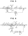
- Fig. 5 illustrates another embodiment of the present invention.
- the PLL circuit of Fig. 5 is characterized in that limiters 9 and 10 are connected to the input portions of the current output type phase comparator 1 in the same configuration of the PLL circuit of Fig. 1.
- limiters 9 and 10 are connected to the input portions of the current output type phase comparator 1 in the same configuration of the PLL circuit of Fig. 1.
- a mixer type circuit using bipolar transistors is employed in the current output type phase comparator 1 and an amplitude of an input signal is smaller than kT/q where q is an amount of electric charges of electrons, k is a Boltzmann's constant, and T is an absolute temperature
- the phase difference conversion gain of the current output type phase comparator 1 has the dependency on the input amplitude.
- the limiters 9 and 10 amplify the input signals to the current output type phase comparator 1 to increase the amplitude of the input signal f RF to a constant amplitude larger than kT/q, so that the phase difference conversion gain of the phase comparator 1 can be made constant.
- Fig. 6 illustrates another embodiment of the present invention.
- the PLL circuit of Fig. 6 is characterized in that low pass filters 11, 12, 13 and 14 are connected in the same configuration as the PLL circuit of Fig. 5.
- the low pass filters 13 and 14 are used to prevent unnecessary harmonics from being inputted to the limiters 9 and 10. Since the limiters 9 and 10 produce the signals having the constant amplitude, the output signals of the limiters 9 and 10 contain unnecessary harmonic components. Accordingly, the low pass filters 11 and 12 removes the unnecessary harmonic components.
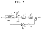
- Fig. 7 illustrates another embodiment of a PLL circuit according to the present invention.
- the PLL circuit of Fig. 7 is characterized in that an amplifier 15 is connected between the coupler 6 and the mixer 7 in the same configuration as the PLL circuit of Fig. 1. By connecting the amplifier 15, the PLL circuit can be operated even when the output of the VCO has a small amplitude.
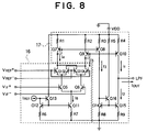
- Fig. 8 illustrates an embodiment of the current output type phase comparator 1.
- Transistors may be of bipolar type.
- VDD is a power supply voltage.
- Numeral 16 denotes a so-called Gilbert multiplier. Detail thereof is described in Chapter 10.3 of "DESIGN TECHNIQUE OF ANALOG INTEGRATED CIRCUIT FOR SUPER LSI (Last Volume)" issued by Baifukan.
- the Gilbert multiplier 16 mixes input signals V IF + and V IF - and reference signals V REF + and V REF - to produce differential currents I 4 and I 5 having phases opposite to each other. Bases of transistors Q2 and Q3 are applied with the signal V REF - having the phase opposite to that of the signal applied to bases of transistors Q1 and Q4.
- a base of transistor Q6 is applied with the signal V IF - having the phase opposite to that of the signal applied to a base of a transistors Q5.
- amplitudes of the input signals V IF + and V IF - and the reference signals V REF + and V REF - are larger than kT/q and a collector current of a transistor Q11 is I 6
- Transistors Q11, Q12 and Q13, resistors R6 and R7 and a constant current source I REF constitute a bias circuit of the Gilbert multiplier 16 using the current mirror circuit.
- the transistor Q11 constitutes a current source for the transistors Q5 and Q6 connected to the collector of the transistor Q11.
- Numeral 17 denotes a charge pump circuit which converts the output differential currents I 4 and I 5 of the Gilbert multiplier 16 into a single-ended output signal to produce it as a current I out .
- transistors Q14, Q15 and Q16 and resistors R8 and R9 also constitute a current mirror circuit.
- a current mirror ratio thereof c
- I 2 c ⁇ I 3
- Fig. 9 illustrates an embodiment of the reset switch. That is, the reset switch corresponds to the reset switch 3 of Fig. 1. Transistors of bipolar type are used.
- VDD is a power supply voltage.
- a constant current source I E is a bias circuit for the reset switch 3 and supplies a bias current to transistors Q17 and Q18.
- a transistor Q18 is turned off, so that currents I 7 and I 8 scarcely flow and transistors Q19 and Q20 are also turned off.
- circuits shown in Figs. 8 and 9 employ bipolar transistors, while transistors of other kinds such as, for example, MOSFET and MESFET may be used to realize the same function.
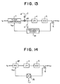
- Fig. 13 illustrates a PLL circuit according to another embodiment of the present invention.
- the PLL circuit of Fig. 13 is characterized in that a frequency divider 41 is connected between the current output type phase comparator 1 and the coupler 6 instead of the mixer 7 in the same configuration as the PLL circuit of Fig. 1.
- a frequency division ratio of the frequency divider 41 is given by f RF /f IF .
- Fig. 14 illustrates a PLL circuit according to still another embodiment of the present invention.
- the PLL circuit includes a current output type phase frequency comparator 42, a low pass filter 4, a VCO 5, a coupler 6 and a mixer 26.
- the current output type phase frequency comparator 42 compares a phase of the input signal f IF with a phase of the reference signal frequency f REF and produces an error output current.
- the current output type phase frequency comparator 42 compares a frequency of the input signal f IF with a frequency of the reference signal frequency f REF and produces an error output current.
- the low pass filter 4 removes unnecessary harmonic components and noise from the output current of the comparator 42 and converts the output current into a voltage to be supplied to the VCO 5.
- An output frequency f RF of the VCO 5 is inputted to the mixer 26 through the coupler 6 and is mixed with the local oscillation signal frequency f LO in the mixer 26.
- the phase comparator is named a phase frequency comparator (PFC). Since the PLL circuit is necessarily locked without the provision of a switch when the PFC is used, the reset switch is not required. However, since the output voltage of the phase comparator is not once reduced to 0 volt by means of the reset switch, the PLL circuit may be operated even if the constant current source for increasing the settling speed is provided, while the settling time is not necessarily shortened.
- PFC phase frequency comparator
- the phase comparator produces the current output and the constant current is further added to the current output, the setting time can be shortened without widening of the band for the PLL circuit. Furthermore, since the settling time shortening circuit and the reset switch are connected to the phase comparator, the circuit configuration suitable for the integrated circuit can be realized.
Landscapes
- Stabilization Of Oscillater, Synchronisation, Frequency Synthesizers (AREA)
- Transceivers (AREA)
Applications Claiming Priority (3)
| Application Number | Priority Date | Filing Date | Title |
|---|---|---|---|
| JP01721797A JP3839117B2 (ja) | 1997-01-30 | 1997-01-30 | Pll回路およびそれを用いた無線通信端末機器 |
| JP1721797 | 1997-01-30 | ||
| JP17217/97 | 1997-01-30 |
Publications (3)
| Publication Number | Publication Date |
|---|---|
| EP0856946A2 true EP0856946A2 (de) | 1998-08-05 |
| EP0856946A3 EP0856946A3 (de) | 1999-08-04 |
| EP0856946B1 EP0856946B1 (de) | 2012-07-04 |
Family
ID=11937784
Family Applications (1)
| Application Number | Title | Priority Date | Filing Date |
|---|---|---|---|
| EP98101219A Expired - Lifetime EP0856946B1 (de) | 1997-01-30 | 1998-01-23 | Phasenstarre Schleife und diese verwendendes Funkkommunikationsgerät |
Country Status (8)
| Country | Link |
|---|---|
| US (4) | US6163585A (de) |
| EP (1) | EP0856946B1 (de) |
| JP (1) | JP3839117B2 (de) |
| KR (1) | KR100328369B1 (de) |
| CN (1) | CN1118137C (de) |
| NO (1) | NO318601B1 (de) |
| SG (1) | SG73493A1 (de) |
| TW (1) | TW407403B (de) |
Cited By (10)
| Publication number | Priority date | Publication date | Assignee | Title |
|---|---|---|---|---|
| WO2000038324A1 (en) * | 1998-12-22 | 2000-06-29 | Xilinx, Inc. | Pll and gain control for clock recovery |
| EP1143623A1 (de) * | 2000-04-07 | 2001-10-10 | Nec Corporation | Adaptiver Phasenvergleicher und Methode zum Phasenvergleich in einer Phase Locked Loop Schaltung |
| EP1179888A1 (de) * | 2000-08-04 | 2002-02-13 | Nec Corporation | PLL Schaltung |
| US6356160B1 (en) | 1999-07-02 | 2002-03-12 | Xilinx, Inc. | Phase lock loop and automatic gain control circuitry for clock recovery |
| EP1220453A1 (de) * | 2000-12-28 | 2002-07-03 | Hitachi, Ltd. | PLL-Schaltung mit reduzierter Einschwingzeit |
| WO2003017492A3 (en) * | 2001-08-16 | 2003-09-25 | Koninkl Philips Electronics Nv | Charge pump |
| US6650720B1 (en) | 1998-12-22 | 2003-11-18 | Xilinx, Inc. | Phase lock loop and transconductance circuit for clock recovery |
| EP1115205A4 (de) * | 1998-09-17 | 2004-03-24 | Hitachi Ltd | Pll-schaltung und funkbetriebenes kommunikationssendegerät mit einer phasenregelschleife |
| WO2004051854A1 (de) * | 2002-11-29 | 2004-06-17 | Infineon Technologies Ag | Phasenregelschleife |
| EP1458099A1 (de) * | 2003-03-14 | 2004-09-15 | STMicroelectronics S.r.l. | Phasenregelschleife mit Aufbereitung des Steuerstroms durch einen schaltbaren Kondensator |
Families Citing this family (21)
| Publication number | Priority date | Publication date | Assignee | Title |
|---|---|---|---|---|
| JP3839117B2 (ja) * | 1997-01-30 | 2006-11-01 | 株式会社ルネサステクノロジ | Pll回路およびそれを用いた無線通信端末機器 |
| JP3727206B2 (ja) * | 1999-11-11 | 2005-12-14 | Necエレクトロニクス株式会社 | クロック乗換回路及びその方法 |
| EP1133060B1 (de) * | 2000-03-10 | 2005-08-17 | Koninklijke Philips Electronics N.V. | Phasenregelschleife zur Erzeugung eines Referenzsignals hoher spektraler Reinheit |
| KR100360411B1 (ko) * | 2000-11-23 | 2002-11-13 | 삼성전자 주식회사 | 오프셋 전류를 자동 조절하는 위상 검출기 및 이를구비하는 위상동기 루프 |
| TWI248721B (en) * | 2001-04-27 | 2006-02-01 | Mediatek Inc | Phase-locked loop with dual-mode phase/frequency detection |
| FI113817B (fi) * | 2002-05-27 | 2004-06-15 | Nokia Corp | Parannettu piirijärjestely vaihelukoksi, vaihelukon toteuttava integroitupiiri, vaihelukkoa hyödyntävä menetelmä ja solukkoverkon päätelaite |
| GB2389253B (en) * | 2002-05-31 | 2005-09-21 | Hitachi Ltd | Transmitter and semiconductor integrated circuit for communication |
| CN100403672C (zh) * | 2002-08-26 | 2008-07-16 | 联发科技股份有限公司 | 使用双模式相位频率检测器的锁相环 |
| TW578387B (en) * | 2002-10-31 | 2004-03-01 | Mediatek Inc | Phase-lock loop applying in wireless communication system and method thereof |
| GB0322538D0 (en) * | 2003-09-26 | 2003-10-29 | Univ Belfast | Phase conjugate circuit |
| US20080036544A1 (en) * | 2006-08-08 | 2008-02-14 | Fucheng Wang | Method for adjusting oscillator in phase-locked loop and related frequency synthesizer |
| US8487707B2 (en) | 2006-08-08 | 2013-07-16 | Mstar Semiconductor, Inc. | Frequency synthesizer |
| JP4752682B2 (ja) * | 2006-08-29 | 2011-08-17 | 横河電機株式会社 | 位相同期ループ回路及び信号発生装置 |
| JP2008219486A (ja) * | 2007-03-05 | 2008-09-18 | Freescale Semiconductor Inc | パワーオン検知回路 |
| JP2011078054A (ja) * | 2009-10-02 | 2011-04-14 | Sony Corp | 電流源、電子機器および集積回路 |
| US8222932B2 (en) * | 2010-02-23 | 2012-07-17 | Agilent Technologies, Inc. | Phase-locked loop with switched phase detectors |
| TWI443492B (zh) * | 2010-05-17 | 2014-07-01 | Mstar Semiconductor Inc | 時脈產生電路與時脈產生方法 |
| JP5573484B2 (ja) * | 2010-08-13 | 2014-08-20 | ソニー株式会社 | 位相同期回路および無線通信装置 |
| US8664985B2 (en) | 2012-02-02 | 2014-03-04 | Mediatek Inc. | Phase frequency detector and charge pump for phase lock loop fast-locking |
| US8934836B2 (en) * | 2012-06-28 | 2015-01-13 | Broadcom Corporation | NFC device with PLL controlled active load modulation |
| CN103684414B (zh) * | 2013-12-30 | 2017-02-08 | 上海贝岭股份有限公司 | 乘法器电路 |
Family Cites Families (40)
| Publication number | Priority date | Publication date | Assignee | Title |
|---|---|---|---|---|
| JPS5683136A (en) | 1979-12-10 | 1981-07-07 | Mitsubishi Electric Corp | Frequency synthesizer |
| US4389622A (en) * | 1981-09-28 | 1983-06-21 | Honeywell Inc. | System for preventing transient induced errors in phase locked loop |
| JPS5989038A (ja) | 1982-11-12 | 1984-05-23 | Victor Co Of Japan Ltd | フエ−ズ・ロツクド・ル−プ回路 |
| US4562410A (en) * | 1983-12-29 | 1985-12-31 | Rca Corporation | Phase lock loop prepositioning apparatus with feedback control |
| JPS61274413A (ja) | 1985-05-29 | 1986-12-04 | Nec Home Electronics Ltd | 振幅制限回路 |
| US4745372A (en) * | 1985-10-17 | 1988-05-17 | Matsushita Electric Industrial Co., Ltd. | Phase-locked-loop circuit having a charge pump |
| JP2758594B2 (ja) * | 1985-11-21 | 1998-05-28 | 日本電気株式会社 | チャージポンプ回路 |
| DE3715929A1 (de) * | 1987-05-13 | 1988-11-24 | Thomson Brandt Gmbh | Schaltungsanordnung zur automatischen umschaltung der regelgeschwindigkeit eines phasenregelkreises |
| US4890072A (en) * | 1988-02-03 | 1989-12-26 | Motorola, Inc. | Phase locked loop having a fast lock current reduction and clamping circuit |
| JPH0262120A (ja) | 1988-08-29 | 1990-03-02 | Matsushita Electric Ind Co Ltd | 位相同期発振器 |
| US4885554A (en) | 1988-12-16 | 1989-12-05 | Tektronix, Inc. | Phase-offset signal generator |
| US4952889A (en) * | 1989-04-28 | 1990-08-28 | Motorola, Inc. | Loop filter modulated synthesizer |
| EP0410029B1 (de) * | 1989-07-25 | 1995-01-04 | Siemens Aktiengesellschaft | Schaltungsanordnung zur Nachlaufsynchronisation |
| US5204975A (en) * | 1989-10-12 | 1993-04-20 | Seiko Epson Corporation | Digitally-corrected temperature-compensated crystal oscillator having a correction-suspend control for communications service |
| US5221911A (en) * | 1991-06-21 | 1993-06-22 | U.S. Philips Corporation | Receiver having pll frequency synthesizer with rc loop filter |
| GB2261345A (en) * | 1991-11-08 | 1993-05-12 | Roke Manor Research | Transceiver having a feedback loop |
| JPH05276030A (ja) | 1992-02-28 | 1993-10-22 | Nec Corp | 位相同期回路 |
| JPH05327492A (ja) | 1992-05-19 | 1993-12-10 | Fujitsu Ltd | Pllシンセサイザ回路 |
| JPH06112820A (ja) | 1992-09-30 | 1994-04-22 | Hitachi Ltd | Pll回路 |
| JPH06268514A (ja) | 1993-03-12 | 1994-09-22 | Toshiba Corp | 位相検波回路 |
| JPH06284030A (ja) | 1993-03-24 | 1994-10-07 | Mitsubishi Electric Corp | フェーズロックドループ検波受信装置 |
| US5313173A (en) * | 1993-04-26 | 1994-05-17 | Ericsson Ge Mobile Communications Inc. | Quadrature modulated phase-locked loop |
| JPH06338786A (ja) | 1993-05-31 | 1994-12-06 | Sanyo Electric Co Ltd | マイクロコンピュータ |
| US5359297A (en) * | 1993-10-28 | 1994-10-25 | Motorola, Inc. | VCO power-up circuit for PLL and method thereof |
| US5511236A (en) * | 1993-12-07 | 1996-04-23 | National Semiconductor Corporation | Half duplex RF transceiver |
| US5424689A (en) * | 1993-12-22 | 1995-06-13 | Motorola, Inc. | Filtering device for use in a phase locked loop controller |
| US5566204A (en) * | 1994-05-02 | 1996-10-15 | Raytheon Company | Fast acquisition clock recovery system |
| US5436597A (en) * | 1994-07-11 | 1995-07-25 | Sierra Semiconductor Corporation | Pro-capture circuit for phase locked loop circuits |
| FI105247B (fi) * | 1994-11-14 | 2000-06-30 | Nokia Mobile Phones Ltd | Menetelmä ja kytkentä radiopuhelimen taajuuksien muodostamiseksi |
| JP3357208B2 (ja) * | 1994-11-25 | 2002-12-16 | アジレント・テクノロジー株式会社 | 同期信号発生装置 |
| US5651035A (en) * | 1995-04-28 | 1997-07-22 | International Microcircuits, Inc. | Apparatus for reducing jitter of a spectrum spread clock signal and method therefor |
| US5576647A (en) * | 1995-06-22 | 1996-11-19 | Marvell Technology Group, Ltd. | Charge pump for phase lock loop |
| KR100193862B1 (ko) * | 1996-03-19 | 1999-06-15 | 윤종용 | 안정된 주파수를 얻기 위한 주파수변환기 |
| JP3839117B2 (ja) * | 1997-01-30 | 2006-11-01 | 株式会社ルネサステクノロジ | Pll回路およびそれを用いた無線通信端末機器 |
| US5834987A (en) * | 1997-07-30 | 1998-11-10 | Ercisson Inc. | Frequency synthesizer systems and methods for three-point modulation with a DC response |
| US5909149A (en) * | 1997-08-29 | 1999-06-01 | Lucent Technologies, Inc. | Multiband phase locked loop using a switched voltage controlled oscillator |
| US6308048B1 (en) * | 1997-11-19 | 2001-10-23 | Ericsson Inc. | Simplified reference frequency distribution in a mobile phone |
| DE69920273T2 (de) * | 1998-11-12 | 2005-09-22 | Broadcom Corp., Irvine | Integrierte tunerarchitektur |
| US6157271A (en) * | 1998-11-23 | 2000-12-05 | Motorola, Inc. | Rapid tuning, low distortion digital direct modulation phase locked loop and method therefor |
| US6091303A (en) * | 1999-04-06 | 2000-07-18 | Ericsson Inc. | Method and apparatus for reducing oscillator noise by noise-feedforward |
-
1997
- 1997-01-30 JP JP01721797A patent/JP3839117B2/ja not_active Expired - Lifetime
-
1998
- 1998-01-22 KR KR1019980001847A patent/KR100328369B1/ko not_active Expired - Fee Related
- 1998-01-23 TW TW087100952A patent/TW407403B/zh not_active IP Right Cessation
- 1998-01-23 EP EP98101219A patent/EP0856946B1/de not_active Expired - Lifetime
- 1998-01-26 SG SG1998000195A patent/SG73493A1/en unknown
- 1998-01-26 CN CN98103709A patent/CN1118137C/zh not_active Expired - Lifetime
- 1998-01-29 NO NO19980399A patent/NO318601B1/no not_active IP Right Cessation
- 1998-01-30 US US09/016,302 patent/US6163585A/en not_active Expired - Lifetime
-
2000
- 2000-12-06 US US09/729,721 patent/US6324219B2/en not_active Expired - Lifetime
-
2001
- 2001-11-27 US US09/993,764 patent/US6639933B2/en not_active Expired - Lifetime
-
2003
- 2003-08-15 US US10/641,136 patent/US7266171B2/en not_active Expired - Fee Related
Cited By (22)
| Publication number | Priority date | Publication date | Assignee | Title |
|---|---|---|---|---|
| EP1115205A4 (de) * | 1998-09-17 | 2004-03-24 | Hitachi Ltd | Pll-schaltung und funkbetriebenes kommunikationssendegerät mit einer phasenregelschleife |
| EP1758255A3 (de) * | 1998-09-17 | 2010-11-24 | Renesas Electronics Corporation | PLL Schaltung und Funkendgerät, das selbige benutzt |
| US7333779B2 (en) | 1998-09-17 | 2008-02-19 | Renesas Technology Corp. | PLL circuit and radio communication terminal apparatus using the same |
| US6996377B1 (en) | 1998-09-17 | 2006-02-07 | Renesas Technology Corp. | PLL circuit and radio communication terminal apparatus using the same |
| US6970683B2 (en) | 1998-09-17 | 2005-11-29 | Renesas Technology Corp. | PLL circuit and radio communication terminal apparatus using the same |
| WO2000038324A1 (en) * | 1998-12-22 | 2000-06-29 | Xilinx, Inc. | Pll and gain control for clock recovery |
| US6650720B1 (en) | 1998-12-22 | 2003-11-18 | Xilinx, Inc. | Phase lock loop and transconductance circuit for clock recovery |
| US6356160B1 (en) | 1999-07-02 | 2002-03-12 | Xilinx, Inc. | Phase lock loop and automatic gain control circuitry for clock recovery |
| EP1143623A1 (de) * | 2000-04-07 | 2001-10-10 | Nec Corporation | Adaptiver Phasenvergleicher und Methode zum Phasenvergleich in einer Phase Locked Loop Schaltung |
| US6466067B2 (en) | 2000-08-04 | 2002-10-15 | Nec Corporation | PLL circuit with shortened lock-up time |
| EP1179888A1 (de) * | 2000-08-04 | 2002-02-13 | Nec Corporation | PLL Schaltung |
| US6912380B2 (en) | 2000-12-28 | 2005-06-28 | Renesas Technology Corp. | PLL circuit and wireless mobile station with that PLL circuit |
| US6608510B2 (en) | 2000-12-28 | 2003-08-19 | Hitachi, Ltd. | PLL circuit and wireless mobile station with that PLL circuit |
| KR100746143B1 (ko) * | 2000-12-28 | 2007-08-03 | 가부시키가이샤 히타치세이사쿠쇼 | Pll 회로 및 무선 통신 단말기기 |
| EP1220453A1 (de) * | 2000-12-28 | 2002-07-03 | Hitachi, Ltd. | PLL-Schaltung mit reduzierter Einschwingzeit |
| WO2003017492A3 (en) * | 2001-08-16 | 2003-09-25 | Koninkl Philips Electronics Nv | Charge pump |
| US6975175B2 (en) | 2001-08-16 | 2005-12-13 | Koninklijke Philips Electronics N.V. | Charge pump |
| KR100906302B1 (ko) * | 2001-08-16 | 2009-07-07 | 엔엑스피 비 브이 | 전하 펌프, 이를 포함하는 클록 복구 회로 및 수신기 |
| WO2004051854A1 (de) * | 2002-11-29 | 2004-06-17 | Infineon Technologies Ag | Phasenregelschleife |
| US7205849B2 (en) | 2002-11-29 | 2007-04-17 | Infineon Technologies Ag | Phase locked loop including an integrator-free loop filter |
| EP1458099A1 (de) * | 2003-03-14 | 2004-09-15 | STMicroelectronics S.r.l. | Phasenregelschleife mit Aufbereitung des Steuerstroms durch einen schaltbaren Kondensator |
| US7005928B2 (en) | 2003-03-14 | 2006-02-28 | Stmicroelectronics S.R.L. | Phase-locked loop circuit with switched-capacitor conditioning of the control current |
Also Published As
| Publication number | Publication date |
|---|---|
| SG73493A1 (en) | 2000-06-20 |
| EP0856946A3 (de) | 1999-08-04 |
| TW407403B (en) | 2000-10-01 |
| CN1189720A (zh) | 1998-08-05 |
| KR19980070697A (ko) | 1998-10-26 |
| US20040032901A1 (en) | 2004-02-19 |
| US7266171B2 (en) | 2007-09-04 |
| NO980399L (no) | 1998-07-31 |
| JPH10215171A (ja) | 1998-08-11 |
| US6163585A (en) | 2000-12-19 |
| NO318601B1 (no) | 2005-04-18 |
| US6324219B2 (en) | 2001-11-27 |
| CN1118137C (zh) | 2003-08-13 |
| KR100328369B1 (ko) | 2002-04-17 |
| JP3839117B2 (ja) | 2006-11-01 |
| US20010008551A1 (en) | 2001-07-19 |
| NO980399D0 (no) | 1998-01-29 |
| US6639933B2 (en) | 2003-10-28 |
| EP0856946B1 (de) | 2012-07-04 |
| US20020044621A1 (en) | 2002-04-18 |
Similar Documents
| Publication | Publication Date | Title |
|---|---|---|
| US6163585A (en) | Phase-locked loop circuit and radio communication apparatus using the same | |
| KR101442265B1 (ko) | 가변 이득 주파수 체배기, 이를 이용하여 송신 신호의 주파수와 이득을 제어하는 방법, 및 가변 이득 주파수 체배기를 갖는 휴대형 트랜시버 | |
| US6091303A (en) | Method and apparatus for reducing oscillator noise by noise-feedforward | |
| Elliott et al. | A polar modulator transmitter for GSM/EDGE | |
| JP4056145B2 (ja) | Pll回路およびそれを用いた無線通信端末機器 | |
| JP3711109B2 (ja) | 無線電話機の電力増幅器への変調の注入を含む連続閉ループ電力制御システム | |
| KR101387262B1 (ko) | 직교 믹서를 위한 lo 신호 생성 시스템 및 방법 | |
| EP0883242A2 (de) | Radioempfänger und Verfahren du dessen Betrieb | |
| WO2003103162A1 (en) | Transmitter and wireless communication apparatus using the transmitter | |
| US7444123B2 (en) | Transmitter and mobile communication terminal using the same | |
| JP4342305B2 (ja) | 特にゼロ中間周波数またはロー中間周波数のrf受信機のための、イメージ周波数を阻止するミクサ回路 | |
| EP0883237A1 (de) | Funkempfänger und Betriebsverfahren dazu | |
| JP2004297454A (ja) | 無線通信システムおよび通信用半導体集積回路 | |
| US20090181626A1 (en) | Transmitter | |
| JP4118309B2 (ja) | Pll回路およびそれを用いた無線通信端末機器 | |
| JP2003500969A (ja) | 遠隔通信ic用の多周波数低電力発振器 | |
| KR20000046539A (ko) | 이동 통신 단말기의 송신 회로 |
Legal Events
| Date | Code | Title | Description |
|---|---|---|---|
| PUAI | Public reference made under article 153(3) epc to a published international application that has entered the european phase |
Free format text: ORIGINAL CODE: 0009012 |
|
| AK | Designated contracting states |
Kind code of ref document: A2 Designated state(s): DE FR GB IT NL SE |
|
| AX | Request for extension of the european patent |
Free format text: AL;LT;LV;MK;RO;SI |
|
| PUAL | Search report despatched |
Free format text: ORIGINAL CODE: 0009013 |
|
| RIC1 | Information provided on ipc code assigned before grant |
Free format text: 6H 03L 7/085 A, 6H 04B 1/40 B, 6H 03L 7/10 B |
|
| AK | Designated contracting states |
Kind code of ref document: A3 Designated state(s): AT BE CH DE DK ES FI FR GB GR IE IT LI LU MC NL PT SE |
|
| AX | Request for extension of the european patent |
Free format text: AL;LT;LV;MK;RO;SI |
|
| 17P | Request for examination filed |
Effective date: 19991012 |
|
| AKX | Designation fees paid |
Free format text: DE FR GB IT NL SE |
|
| RAP1 | Party data changed (applicant data changed or rights of an application transferred) |
Owner name: TTPCOM LIMITED Owner name: HITACHI, LTD. |
|
| RAP1 | Party data changed (applicant data changed or rights of an application transferred) |
Owner name: TTPCOM LIMITED Owner name: RENESAS TECHNOLOGY CORP. |
|
| RAP1 | Party data changed (applicant data changed or rights of an application transferred) |
Owner name: TTPCOM LIMITED Owner name: RENESAS ELECTRONICS CORPORATION |
|
| GRAP | Despatch of communication of intention to grant a patent |
Free format text: ORIGINAL CODE: EPIDOSNIGR1 |
|
| GRAS | Grant fee paid |
Free format text: ORIGINAL CODE: EPIDOSNIGR3 |
|
| GRAA | (expected) grant |
Free format text: ORIGINAL CODE: 0009210 |
|
| AK | Designated contracting states |
Kind code of ref document: B1 Designated state(s): DE FR GB IT NL SE |
|
| REG | Reference to a national code |
Ref country code: GB Ref legal event code: FG4D |
|
| REG | Reference to a national code |
Ref country code: NL Ref legal event code: T3 |
|
| REG | Reference to a national code |
Ref country code: DE Ref legal event code: R096 Ref document number: 69842783 Country of ref document: DE Effective date: 20120830 |
|
| REG | Reference to a national code |
Ref country code: SE Ref legal event code: TRGR |
|
| PLBE | No opposition filed within time limit |
Free format text: ORIGINAL CODE: 0009261 |
|
| STAA | Information on the status of an ep patent application or granted ep patent |
Free format text: STATUS: NO OPPOSITION FILED WITHIN TIME LIMIT |
|
| 26N | No opposition filed |
Effective date: 20130405 |
|
| REG | Reference to a national code |
Ref country code: DE Ref legal event code: R097 Ref document number: 69842783 Country of ref document: DE Effective date: 20130405 |
|
| REG | Reference to a national code |
Ref country code: FR Ref legal event code: PLFP Year of fee payment: 19 |
|
| PGFP | Annual fee paid to national office [announced via postgrant information from national office to epo] |
Ref country code: DE Payment date: 20160315 Year of fee payment: 19 Ref country code: IT Payment date: 20160126 Year of fee payment: 19 |
|
| PGFP | Annual fee paid to national office [announced via postgrant information from national office to epo] |
Ref country code: NL Payment date: 20160128 Year of fee payment: 19 Ref country code: GB Payment date: 20160203 Year of fee payment: 19 Ref country code: FR Payment date: 20160129 Year of fee payment: 19 Ref country code: SE Payment date: 20160121 Year of fee payment: 19 |
|
| REG | Reference to a national code |
Ref country code: DE Ref legal event code: R119 Ref document number: 69842783 Country of ref document: DE |
|
| REG | Reference to a national code |
Ref country code: NL Ref legal event code: MM Effective date: 20170201 |
|
| GBPC | Gb: european patent ceased through non-payment of renewal fee |
Effective date: 20170123 |
|
| REG | Reference to a national code |
Ref country code: DE Ref legal event code: R082 Ref document number: 69842783 Country of ref document: DE Representative=s name: BETTEN & RESCH PATENT- UND RECHTSANWAELTE PART, DE |
|
| REG | Reference to a national code |
Ref country code: FR Ref legal event code: ST Effective date: 20170929 |
|
| PG25 | Lapsed in a contracting state [announced via postgrant information from national office to epo] |
Ref country code: FR Free format text: LAPSE BECAUSE OF NON-PAYMENT OF DUE FEES Effective date: 20170131 |
|
| PG25 | Lapsed in a contracting state [announced via postgrant information from national office to epo] |
Ref country code: DE Free format text: LAPSE BECAUSE OF NON-PAYMENT OF DUE FEES Effective date: 20170801 Ref country code: GB Free format text: LAPSE BECAUSE OF NON-PAYMENT OF DUE FEES Effective date: 20170123 Ref country code: NL Free format text: LAPSE BECAUSE OF NON-PAYMENT OF DUE FEES Effective date: 20170201 Ref country code: SE Free format text: LAPSE BECAUSE OF NON-PAYMENT OF DUE FEES Effective date: 20170124 |
|
| PG25 | Lapsed in a contracting state [announced via postgrant information from national office to epo] |
Ref country code: IT Free format text: LAPSE BECAUSE OF NON-PAYMENT OF DUE FEES Effective date: 20170123 |
|
| P01 | Opt-out of the competence of the unified patent court (upc) registered |
Effective date: 20230520 |