EP0858095A2 - Procédés et appareils pour pulvérisation magnétron à balayage linéaire - Google Patents
Procédés et appareils pour pulvérisation magnétron à balayage linéaire Download PDFInfo
- Publication number
- EP0858095A2 EP0858095A2 EP98300888A EP98300888A EP0858095A2 EP 0858095 A2 EP0858095 A2 EP 0858095A2 EP 98300888 A EP98300888 A EP 98300888A EP 98300888 A EP98300888 A EP 98300888A EP 0858095 A2 EP0858095 A2 EP 0858095A2
- Authority
- EP
- European Patent Office
- Prior art keywords
- target
- magnet assembly
- assembly
- plasma
- source
- Prior art date
- Legal status (The legal status is an assumption and is not a legal conclusion. Google has not performed a legal analysis and makes no representation as to the accuracy of the status listed.)
- Withdrawn
Links
Images




Classifications
-
- H—ELECTRICITY
- H01—ELECTRIC ELEMENTS
- H01J—ELECTRIC DISCHARGE TUBES OR DISCHARGE LAMPS
- H01J37/00—Discharge tubes with provision for introducing objects or material to be exposed to the discharge, e.g. for the purpose of examination or processing thereof
- H01J37/32—Gas-filled discharge tubes
- H01J37/34—Gas-filled discharge tubes operating with cathodic sputtering
- H01J37/3411—Constructional aspects of the reactor
- H01J37/345—Magnet arrangements in particular for cathodic sputtering apparatus
- H01J37/3455—Movable magnets
-
- C—CHEMISTRY; METALLURGY
- C23—COATING METALLIC MATERIAL; COATING MATERIAL WITH METALLIC MATERIAL; CHEMICAL SURFACE TREATMENT; DIFFUSION TREATMENT OF METALLIC MATERIAL; COATING BY VACUUM EVAPORATION, BY SPUTTERING, BY ION IMPLANTATION OR BY CHEMICAL VAPOUR DEPOSITION, IN GENERAL; INHIBITING CORROSION OF METALLIC MATERIAL OR INCRUSTATION IN GENERAL
- C23C—COATING METALLIC MATERIAL; COATING MATERIAL WITH METALLIC MATERIAL; SURFACE TREATMENT OF METALLIC MATERIAL BY DIFFUSION INTO THE SURFACE, BY CHEMICAL CONVERSION OR SUBSTITUTION; COATING BY VACUUM EVAPORATION, BY SPUTTERING, BY ION IMPLANTATION OR BY CHEMICAL VAPOUR DEPOSITION, IN GENERAL
- C23C14/00—Coating by vacuum evaporation, by sputtering or by ion implantation of the coating forming material
- C23C14/22—Coating by vacuum evaporation, by sputtering or by ion implantation of the coating forming material characterised by the process of coating
- C23C14/34—Sputtering
- C23C14/35—Sputtering by application of a magnetic field, e.g. magnetron sputtering
-
- H—ELECTRICITY
- H01—ELECTRIC ELEMENTS
- H01J—ELECTRIC DISCHARGE TUBES OR DISCHARGE LAMPS
- H01J37/00—Discharge tubes with provision for introducing objects or material to be exposed to the discharge, e.g. for the purpose of examination or processing thereof
- H01J37/32—Gas-filled discharge tubes
- H01J37/34—Gas-filled discharge tubes operating with cathodic sputtering
- H01J37/3402—Gas-filled discharge tubes operating with cathodic sputtering using supplementary magnetic fields
- H01J37/3405—Magnetron sputtering
- H01J37/3408—Planar magnetron sputtering
Definitions
- This invention relates to deposition of sputtered films on substrates and, more particularly, to linear scan magnetron sputtering methods and apparatus which provide long target life and depositional thickness uniformity on large area substrates.
- Sputter deposition also known as sputter coating, is a technique for depositing thin films of desired materials on a substrate such as, for example, a glass panel for a flat panel display, a magnetic disk for a hard disk drive or a semiconductor wafer.
- a substrate such as, for example, a glass panel for a flat panel display, a magnetic disk for a hard disk drive or a semiconductor wafer.
- ions of an inert gas from a plasma are accelerated toward a target of the material to be deposited. Free atoms of the target material are expelled when the ions collide with the target. A portion of the free atoms are collected on the surface of the substrate and form a thin film.
- Magnetron sputtering uses a magnetic field to concentrate the sputtering action. Magnets are positioned behind the target, and magnetic field lines penetrate the target and form arcs over its surface. The magnetic field helps to confine electrons in an area near the surface of the target. The resulting increased concentration of electrons produces a high density of ions and enhances the efficiency of the sputtering process.
- both fixed and movable magnet structures have been utilized in magnetron sputtering.
- the target is circular and the magnet structure rotates with respect to the center of the target.
- the target is rectangular or square and the magnet structure is scanned along a linear path with respect to the target.
- the target is rectangular and the substrate is moved in a plane parallel to the surface of the target during sputtering.
- the second type of sputtering system is disclosed, for example, in U.S. Patent No. 5,382,344 issued January 17, 1995 to Hosokawa et al and U.S. Patent No. 5,565,071 issued October 15, 1996 to Demaray et al.
- a sputter cathode wherein target segments are mounted on a mounting plate by locating studs is disclosed in U.S. Patent No. 5,536,380 issued July 16, 1996 to Ocker et al.
- Each target segment includes a target backplate and a target bonded to the backplate.
- Linear scan sputtering systems typically utilize a magnet assembly which produces a closed-loop plasma in the shape of an elongated oval, often referred to as a racetrack-shaped plasma.
- the magnet assembly is scanned with respect to the target in a direction perpendicular to the long dimension of the racetrack-shaped plasma.
- the resulting erosion of the target tends to be greatest at the ends of the plasma, thus producing erosion grooves along each edge of the target parallel to the scan direction.
- sputtering must be stopped before the erosion pattern has consumed the full thickness of the target material at any point.
- the target must be replaced when the erosion at any point approaches a substantial fraction of the target's initial thickness.
- only a certain number of substrates can be coated from one target. By making the erosion of the target more uniform, a larger percentage of the target material may be utilized before it is necessary to replace the target.
- the linear scanning sputter source typically has a large rectangular or square target attached to a water-cooled backing plate. This structure operates at cathode potential, typically several hundred volts negative with respect to ground.
- a racetrack-shaped magnet assembly creates a magnetic field at the target surface that is sufficient to sustain a plasma when the appropriate electric field is provided.
- the electric field is created by operating the target structure at cathode potential in a chamber held at ground potential.
- the electric field at the target surface is influenced by the size and shape of the chamber and by the characteristics of the plasma which is formed.
- the combination of magnetic and electric fields in a near vacuum causes the sputtering action to occur.
- Depositional thickness uniformity is an important requirement of sputtering systems. For large area substrates, uniform deposition is achieved by using large targets and linearly scanning the magnet assembly with respect to the target, producing uniform erosion of the target surface and uniform coating of the substrate. However, the inherent geometry of a large area sputtering system produces effects which limit thickness uniformity.
- the magnet assembly is linearly scanned parallel to the target surface and perpendicular to the long dimension of the magnet assembly. This motion causes the plasma, which is formed a few millimeters away from the target surface, to sweep across the target surface.
- the geometry of the sputtering chamber affects the depositional thickness uniformity. In particular, when the chamber walls are relatively close to the ends of the racetrack-shaped plasma, the deposited films are relatively thin in the center of the substrate and relatively thick at the edges. It is desirable to provide a sputtering system which achieves depositional thickness uniformity.
- a magnetron sputtering source for depositing a material onto a substrate.
- the magnetron sputtering source comprises a target having a surface, spaced from the substrate, from which the material is sputtered, a magnet assembly disposed in proximity to the target for confining a plasma at the surface of the target and a drive assembly for scanning the magnet assembly relative to the target.
- the sputtering source further comprises an anode, adapted to be coupled to a voltage source, for maintaining substantially constant plasma characteristics as the magnet assembly is scanned relative to the target.
- the magnet assembly is linearly scanned by the drive assembly along a scan direction relative to the target, and the plasma defines an elongated plasma track having a long dimension perpendicular to the scan direction of the magnet assembly.
- the anode comprises first and second stationary electrodes disposed at or near opposite ends of the path followed by the magnet assembly during scanning. Voltages coupled to the electrodes from the voltage source are varied as the magnet assembly is scanned along the path to maintain substantially constant plasma characteristics as the plasma position changes.
- the anode comprises a stationary electrode disposed between the target and the substrate.
- the stationary electrode is transmissive of the target material being deposited on the substrate.
- the stationary electrode may comprise a plurality of spaced-apart anode wires or a mesh disposed between the target and the substrate.
- a movable anode is scanned with the magnet assembly and maintains a fixed position relative to the magnet assembly during scanning.
- the anode may be disposed between the target and the substrate and may be mechanically coupled to the drive assembly.
- the anode is mechanically coupled to the magnet assembly around opposite edges of the target.
- the anode may comprise elongated conductors disposed between the target and the substrate and spaced on opposite sides of the plasma.
- the anode may comprise a tube for circulating a cooling fluid or for delivering a process gas to the region of the plasma.
- the magnetron sputtering source may further include at least one process gas tube, movable with the anode, for delivering a process gas to the region of the plasma.
- a baffle structure may be disposed around the process gas tube or around the anode when it is used to deliver a process gas.
- the baffle structure directs a substantially uniform sheet of process gas in a selected direction, such as toward the substrate.
- the movable anode maintains substantially constant plasma characteristics as the plasma is scanned with respect to the target and the substrate.
- a magnetron sputtering source for depositing a material onto a substrate.
- the magnetron sputtering source comprises a target having a surface, spaced from the substrate, from which the material is sputtered, a magnet assembly disposed in proximity to the target for confining a plasma at the surface of the target and a drive assembly for scanning the magnet assembly relative to the target along a scan direction.
- the magnet assembly comprises a plurality of magnet elements. At least some of the magnet elements of the magnet assembly have different spacings from the surface of the target.
- the magnet assembly has an elongated configuration. Magnet elements near the ends of the magnet assembly may have a greater or a lesser spacing from the surface of the target than magnet elements near the center of the magnet assembly.
- the magnet assembly may comprise at least two sections connected by hinges. Preferably, the spacings between the magnet elements and the surface of the target are selected to produce substantially uniform deposition of the target material on the substrate.
- a sputtering target assembly for a magnetron sputtering source.
- the sputtering target assembly comprises a plurality of individual backing elements, each including a passage for a cooling fluid, target elements bonded to the surfaces of the backing elements and a support structure for mounting the backing elements and the target elements in predetermined positions in the target assembly.
- the support structure may include support elements for supporting opposite edges of the target assembly and a key retained in slots in adjacent backing elements.
- the sputtering target assembly includes four target elements and four backing elements, and each of the target elements has a square configuration.
- a method for operating a magnetron sputtering source comprises a target having a surface from which material is sputtered, a magnet assembly for confining a plasma at the surface of a target and a drive assembly for linearly scanning the magnet assembly relative to the target.
- the target is moved from a first fixed position relative to the magnet assembly to a second fixed position relative to the magnet assembly at least once during the operating life of the target.
- the first and second fixed positions are selected to extend the life of the target.
- the target is rotated about its center.
- the first and second fixed positions of the target assembly may differ by ⁇ 90% relative to the center of the target.
- a method for operating a magnetron sputtering source comprises a target having a surface from which material is sputtered, a magnet assembly for confining a plasma at the surface of the target and a drive assembly for linearly scanning the magnet assembly relative to the target.
- the speed of scanning of the magnet assembly is varied with respect to the target during scanning to obtain a desired sputtered film thickness characteristic on the target.
- the scanning speed is reduced near opposite edges of the target to achieve a substantially uniform sputtered film thickness.
- a magnetron sputtering source for depositing a material onto a substrate.
- the magnetron sputtering source comprises a movable assembly and a drive assembly for scanning the movable assembly along a prescribed linear path relative to the substrate.
- the movable assembly comprises a target having a surface from which the material is sputtered, a magnet assembly disposed in proximity to the target for confining a plasma at the surface of the target and an anode for producing electric fields in a region of the plasma.
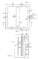
- FIGS. 1-3 A simplified schematic diagram of a linear scan magnetron sputter coating system is shown in FIGS. 1-3.
- a substrate 10 such as for example a glass panel, is positioned in a vacuum chamber 12.
- a linear scan magnetron sputter source 20 comprises a sputtering target assembly including a target 22 of a material to be deposited on substrate 10, a magnet assembly 24, and a drive assembly 30 which causes the magnet assembly 24 to be scanned along a linear path with respect to target 22.
- the structure of the target assembly is described below.
- the drive assembly 30 may, for example, include a drive motor 32 connected to a ball shaft 34.
- the magnet assembly 24 is connected to ball shaft 34 by a ball nut 36.
- the magnet assembly When the drive motor 32 is energized, the magnet assembly is scanned along a linear path, in a scan direction 38, below target 22 over substantially the entire area of target 22.
- the magnet assembly 24 is scanned with a reciprocating linear movement and changes direction at or near opposite edges 26 and 28 of the target.
- An array of magnet elements 40 in magnet assembly 24 produces magnetic fields which penetrate target 22 and form arcs over a surface 42 of target 22 facing substrate 10 (see FIG. 19).
- the magnetic field helps to confine electrons in an area near the surface 42 of the target.
- the increased concentration of electrons produces high densities of inert gas ions, typically argon, and enhances the efficiency of the sputtering process.
- the region of most intense ionization forms a plasma 50 near the surface 42 of target 22.
- the plasma 50 follows a closed-loop plasma track having the shape of an elongated oval.
- the plasma may be described as racetrack shaped.
- the racetrack-shaped plasma 50 is disposed with its long dimension perpendicular to the scan direction 38 of magnet assembly 24.
- the ends of the racetrack-shaped plasma 50 may be straight or curved and are located at or near edges 46 and 48 of target 22.
- the plasma 50 follows the instantaneous position of the magnet assembly 24 and sputters areas of the target 22.
- the size and shape of plasma track 50 and the path followed by magnet assembly 24 during scanning are selected such that the plasma is scanned over substantially the entire area of target 22 and sputters material from target 22. A portion of the sputtered material is deposited on substrate 10.
- sputter coating of large area substrates may be required.
- sputter coating of glass panels having dimensions on the order of 650 x 650 millimeters (mm) may be required.
- the sputtering target 22 is somewhat larger than the substrate to ensure uniform depositional thickness of the deposited coating.
- targets having dimensions on the order of 34 inches on a side may be required.
- the target material is bonded to a water-cooled backing plate and is required to maintain dimensional stability and flatness over its operating life.
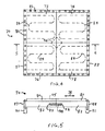
- a target assembly 70 includes a first section 72, a second section 74, a third section 76, and a fourth section 78.
- Each section includes a target element 80 bonded to a backing plate 82.
- the target element 80 is the material to be sputtered onto the substrate.
- the backing plate 82 forms a support for target element 80 and typically includes a passage 84 for circulation of a cooling fluid.
- the target element 80 may be bonded to backing plate 82 by solder, typically an indium alloy solder.
- the backing plate 82 may, for example, be copper.
- the target elements and the backing plates are typically rectangular or square.
- the backing plate 82 extends beyond target element 80 along two outside edges of target assembly 70 and is provided with mounting holes 86.
- the target assembly 70 is supported at opposite edges 87 and 88 by support elements 90 and 91, respectively.
- the target assembly 70 is supported only along edges 87 and 88 at the ends of the scan path, leaving the remainder of the front and back surfaces exposed.
- the backing plate 82 is provided with mounting holes 86 along two outside edges, as shown in FIG. 4, to permit the target assembly to be rotated as described below.
- the target sections may be spaced apart by a sufficient distance, typically on the order of 0.5 mm, to allow for unrestricted thermal expansion and contraction of the target sections. The relatively small spacing between target sections does not appreciably affect the uniformity of the deposited film on the substrate.
- Adjoining edges of the target sections adjacent to the center of the target assembly may be provided with slots 92 for a key 94.
- the key 94 establishes the desired relative positions of the target sections in the target assembly and prevents relative movement of the target sections perpendicular to a target surface 95.
- the key 94 may, for example, have dimensions of 2.0 x 2.0 x 0.25 inches.
- the target assembly 70 is typically mounted vertically in a sputter coating system.
- the mounting arrangement, including support elements 90 and 91, and key 94 retains the target sections In fixed relative positions in the target assembly 70. With the exception of the target surface 95 which faces the substrate, the target assembly is preferably surrounded by a grounded shield (not shown).
- the configuration of the target assembly shown in FIGS. 4 and 5 and described above limits bowing of the target by providing small target sections.
- the reduction of bowing as compared with a single large target simplifies fabrication and the bonding process, and reduces the chance of breakage when the target material is a ceramic such as indium tin oxide.
- the target assembly may be fabricated with two or more target sections and that the target sections may have any desired size or shape.
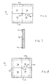
- FIGS. 6-8 A further aspect of the invention is illustrated in FIGS. 6-8. For simplicity of illustration, only the target elements of each target section are shown. Also. to assist in understanding the invention, the thickness of the target elements relative to their lateral dimensions is exaggerated in FIG. 7.
- a typical erosion pattern 96 for a linear scan magnetron sputtering source is shown in FIGS. 6 and 7. The target is eroded over substantially its entire surface (FIG. 7). However, erosion grooves 100 and 102 form along opposite edges of the target assembly 70 parallel to the scan direction 38 of the magnet assembly. The formation of erosion grooves 100 and 102 may be understood with reference to FIG. 1.
- the length of plasma above these regions is greater than in the center portion of the plasma 50, resulting in increased erosion.
- the erosion grooves 100 and 102 reach a depth that is a substantial fraction of the target thickness, the target is ordinarily replaced in order to avoid the risk of contamination of the substrate.
- the target assembly is moved, at least once during its operating life, from a first fixed position relative to the magnet assembly to a second fixed position relative to the magnet assembly.
- the target assembly 70 is rotated by 90% about center 104 relative to the position shown in FIG. 6. This causes erosion grooves 100 and 102 to be oriented perpendicular to scan direction 38 of magnet assembly 24, as shown in FIG. 8.
- new erosion grooves 110 and 112 form on the other two edges of the target assembly parallel to scan direction 38.
- Erosion grooves are formed along all four sides of the target, and utilization of the center region of the target is effectively doubled.
- the target assembly is rotated at a time during its life when erosion grooves 100 and 102 would otherwise require replacement of the target.
- the target assembly can be rotated more frequently if desired.
- the target assembly 70 may be rotated about center 104 by ⁇ 90% with respect to the initial position shown in FIG. 6.
- a linear scan magnetron sputtering system with a large target area and chamber walls close to the edges of the substrate produces deposited films that are relatively thick near the outside edges of the substrate and relatively thin in a center region of the substrate. It is believed that this is due to the fact that the electrons in the plasma near the center of the target cannot escape as easily as electrons in the plasma near the edges of the target. Less electron loss means that the plasma becomes easier to sustain. Hence the plasma voltage drops and sputter yield correspondingly drops.
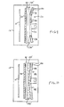
- the plasma intensity may be reduced by reducing the magnetic fields near the ends of the magnet assembly relative to the magnetic fields in the center region. This may be accomplished by making the spacing between the magnet assembly and the target surface relatively small in the center region of the target and larger near the ends. Magnet assemblies having variable spacing from the target surface are shown in FIGS. 9 and 10. Like elements in FIGS. 1-3, 9 and 10 have the same reference numerals.
- a magnet assembly 130 includes a center section 132 and end sections 134 and 136 connected to opposite ends of center section 132.
- Each of the sections 132, 134 and 136 of magnet assembly 130 includes a plurality of magnet elements 140 which generate magnetic fields at the surface of target 22 for producing plasma 50.
- the magnet elements 140 of sections 134 and 136 near the ends of magnet assembly 130 are spaced farther from target 22 than the magnet elements 140 of center section 132.
- the end sections 134 and 136 may be linear or nonlinear and may be connected to center section 132 in a fixed orientation or may be connected by hinges to permit adjustment of the spacings between the magnet elements 140 of end sections 134 and 136 and target 22.
- center section 132 and end sections 134 and 136 may be varied within the scope of the invention.
- the magnet elements 140 of sections 134 and 136 are closer to target 22 than the magnet elements 140 of center section 132, as illustrated in phantom by end sections 134R and 136R in FIG. 9. This configuration may be used to improve thickness uniformity in some applications.
- a magnet assembly 146 includes a first section 148 and a second section 150. Each section includes magnet elements 140.
- the sections 148 and 150 of magnet assembly 146 are oriented such that the spacings between magnet elements 140 and target 22 are less near the center of the magnet assembly than the spacings of magnet elements near the ends.
- the sections 148 and 150 may be linear or nonlinear and may be connected in a fixed orientation or may be hinged.
- the sections 148 and 150 of magnet assembly 146 may be oriented such that the spacings between magnet elements 140 and target 22 are greater near the center of the magnet assembly than the spacings of magnet elements 140 near the ends. This configuration is illustrated in phantom in FIG. 10 by sections positions 148R and 150R of the magnet assembly 146. This configuration may provide improved uniformity in certain applications.
- FIGS. 9 and 10 wherein the magnet elements near the ends of the magnet assembly are spaced from target 22 by a greater or a lesser distance than magnet elements near the center of the magnet assembly, provides improved uniformity along a direction parallel to the long dimension of the magnet assembly, as compared with a magnet assembly having uniform spacing from the target.
- This configuration does not require magnet elements with different sizes, strengths and/or spacings to achieve uniformity.
- the magnet assembly configurations shown in FIGS. 9 and 10 address the issue of depositional thickness uniformity along the long dimension of the magnet assembly.
- variations in thickness uniformity have also been observed along the scan direction of the magnet assembly (perpendicular to the long dimension of the magnet assembly). This variation is believed to be due to the fact that the spacing between the plasma and the grounded vacuum chamber wall varies as the magnet assembly is scanned, causing a variation in electric field in the region of the plasma. The variation in electric field, in turn, causes a variation in sputtering rate.
- FIGS. 11 and 12 A further aspect of the invention is described with reference to FIGS. 11 and 12. Like elements in FIGS. 1-3, 11, and 12 have the same reference numerals.
- the drive assembly is omitted from FIGS. 11 and 12 for simplicity of illustration.
- a stationary electrode 200 is positioned within vacuum chamber 12 between target 22 and substrate 10.
- the stationary electrode 200 must be substantially transparent to the material sputtered from target 22 onto substrate 10. This may be achieved, for example, by utilizing a series of spaced-apart anode wires or by a conductive mesh with relatively large open areas.
- the stationary electrode 200 comprises spaced-apart, parallel anode wires 204, 206, etc.
- the anode wires may be connected to the vacuum chamber walls or to a separate voltage source.
- the stationary electrode between target 22 and substrate 10 provides a fixed potential, such as ground potential, with little variation in distance from plasma 50 as the magnet assembly 24 is scanned over target 22. Thus, a substantially constant electric field is present in the region of the plasma 50 at all times during scanning.
- the substantially constant electric field produces substantially constant plasma characteristics as the magnet assembly 24 is scanned over target 22.
- the diameters of the anode wires 204, 206, etc. and the spacing between anode wires are selected to provide a substantially constant electric field (i.e., constant within about 5%) in the region of plasma 50 as the magnet assembly 24 is scanned over target 22 and to permit most of the sputtered material from target 22 to reach substrate 10.
- FIGS. 13 and 14 Like elements shown in FIGS. 1-3, 13, and 14 have the same reference numerals.
- the drive assembly is omitted from FIGS. 13 and 14 for simplicity of illustration.
- the configuration of FIGS. 13 and 14 utilizes a first stationary electrode 220 and a second stationary electrode 222 positioned along opposite edges of target 22 at or near opposite ends of the path followed by magnet assembly 24 during scanning.
- the stationary electrodes 220 and 222 are preferably located adjacent to opposite edges 26 and 28, respectively, of target 22 and adjacent to the region between target 22 and substrate 10. Scanning of magnet assembly 24 and plasma 50 is illustrated in FIGS. 13 and 14 by plasma position 50. at the left side of target 22 and plasma position 50.. at the right side of target 22.
- Electrodes 220 and 222 are preferably connected to a variable voltage source 230.
- the voltages applied to electrodes 220 and 222 by voltage source 230 may be varied in synchronism with scanning of magnet assembly 24 and plasma 50 to produce substantially constant plasma characteristics during scanning.
- An example of suitable waveforms for application to electrodes 220 and 222 is shown in FIG. 15.
- a waveform 240 is applied to electrode 220, and a waveform 242 is applied to electrode 222.
- Each waveform may, for example, vary linearly between 0 volts when the plasma 50 is farthest from the electrode in the scan cycle and -100 volts when the plasma 50 is closest to the electrode during the scan cycle.
- FIG. 15 An example of suitable waveforms for application to electrodes 220 and 222 is shown in FIG. 15.
- a waveform 240 is applied to electrode 220
- a waveform 242 is applied to electrode 222.
- Each waveform may, for example, vary linearly between 0 volts when the plasma 50 is farthest from the electrode in the scan cycle and -100 volts when the plasma 50 is closest
- times T 1 and T 6 correspond to times when the plasma 50 is near electrode 220; times T 2 and T 5 correspond to times when the plasma 50 is at the middle of the scan cycle; and time T 3 corresponds to a time when the plasma 50 is located near electrode 222.
- the electrodes 220 and 222 may be shaped to enhance the thickness uniformity of the sputtered film. Furthermore, electrodes 220 and 222 may be segmented, with different voltages applied to different segments to enhance thickness uniformity of the sputtered film.
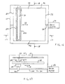
- FIGS. 16-18 A further embodiment of the linear scan magnetron sputtering system of the invention is shown in FIGS. 16-18. Like elements in FIGS. 1-3 and 16-18 have the same reference numerals.
- a scanning anode 250 is mechanically coupled to the drive assembly 30 and is scanned with the magnet assembly 24.
- the anode 250 is positioned between target 22 and substrate 10 in alignment with magnet assembly 24.
- anode 250 remains in a fixed relationship with respect to plasma 50 during scanning.
- the anode 250 preferably comprises one or more elongated conductors of relatively small diameter so as to avoid significantly blocking sputtered target material from reaching substrate 10.
- FIGS. 16-18 A further embodiment of the linear scan magnetron sputtering system of the invention is shown in FIGS. 16-18. Like elements in FIGS. 1-3 and 16-18 have the same reference numerals.
- a scanning anode 250 is mechanically coupled to the drive assembly 30 and is scanned with the magnet assembly 24.
- the anode 250 is
- the anode 250 is mechanically coupled to magnet assembly 24 by support members 254 and 256 to form a moving assembly 260.
- Support member 254 is connected between one end of anode 250 and one end of magnet assembly 24 around edge 26 of target 22; and support member 256 is connected between the other end of anode 250 and the other end of magnet assembly 24 around edge 28 of target 22.
- the support elements 254 and 256 are preferably non-conducting, so that anode 250 and magnet assembly 24 may be maintained at different electrical potentials.
- the anode 250 may be connected to a fixed voltage, such as ground, and maintains a substantially constant electric field in the region of plasma 50, and thereby maintains substantially constant plasma characteristics, during scanning by magnet assembly 24.
- the embodiment of FIGS. 16-18 provides more constant electric fields in the region of plasma 50, and therefore more constant plasma characteristics, than the embodiments of FIGS. 11-14, because the anode 250 has a fixed physical relationship with plasma 50 during scanning.
- anode 250 may be connected directly to drive assembly 30 rather than to magnet assembly 24 or may be connected to a second drive assembly synchronized with drive assembly 30.
- the principal requirement is that the anode 250 move in synchronism with magnet assembly 24 during scanning, so that a fixed physical relationship is maintained between anode 250 and plasma 50.
- the anode 250 may utilize two parallel conductors as shown in FIG. 16, a single conductor or more than two conductors.
- the principal requirements are that the anode maintain substantially constant plasma characteristics during scanning, without substantially blocking sputtered target material from reaching substrate 10.
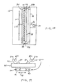
- FIG. 19 A partial schematic elevation view of the sputtering source is shown. Like elements in FIGS. 16-19 have the same reference numerals.
- the drive assembly is omitted from FIG. 19 for simplicity of illustration.
- the anode 250 is configured as a conductive tube, and a cooling gas or liquid is circulated through the conductive tubes.
- the conductive tube is maintained at a desired potential, such as ground, and the circulating fluid limits temperature rise of the anode.
- the moving assembly 260 which includes magnet assembly 24 and anode 250, may further be provided with one or more process gas tubes 270.
- the process gas tubes may be located adjacent to anode 250 between target 22 and substrate 10.
- the process gas tubes 270 may include perforations for delivering a process gas to the region of plasma 50, typically directed toward the substrate 10.
- the process gas may be utilized in the sputtering process. Examples of process gases utilized in sputtering include nitrogen and oxygen.
- the configuration of FIG. 19 has the advantage that the process gas is delivered directly to the region of plasma 50 during scanning of magnet assembly 24. It will be understood that any number of process gas tubes may be utilized.
- process gas tubes may deliver different process gases.
- the anode may be configured as a conductive tube having perforations for delivering a process gas to a region of plasma 50.
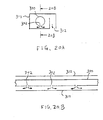
- a tube 300 for delivering a process gas is provided with perforations 302 spaced apart along its length.
- the tube 300 may correspond to anode 250 or to process gas tube 270 described above.
- a baffle structure 310 is disposed around tube 300 along its length.
- the baffle structure 310 may provide a serpentine path between perforations 302 in tube 302 in tube 300 and an outlet 312.
- the baffle structure 310 spreads the gas flow delivered by tube 300 through perforations 302 and provides a substantially uniform, linear curtain of process gas directed preferentially in a selected direction, such as toward the substrate.
- the process gas is required to react with material of the target at the substrate surface.
- magnesium oxide may be formed on the substrate from a magnesium target and oxygen gas delivered through tube 300. Where the process gas is not directed toward the substrate, magnesium oxide may form on the target surface. Magnesium oxide contamination of the target is likely to interfere with the sputtering process.
- the configuration shown in FIGS. 20A and 20B and described above substantially reduces the amount of process gas that reaches the target surface. It will be understood that a variety of different baffle structures, shapes and configurations may be utilized to direct the gas flow toward the substrate.
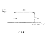
- the scan speed of the magnet assembly 24 is substantially constant between the ends of the scan path.
- the scan speed may be varied as a function of magnet assembly position to control uniformity of the deposited film. By decreasing the scan speed in a specified region, the film thickness is increased. Conversely, by increasing the scan speed in a specified region, the film thickness is decreased.
- An example of a scan speed profile is shown in FIG. 21. Scan speed is plotted as a function of position along the scan path. With reference to FIG. 16, scan position 320 corresponds to edge 26 of target 22, and scan position 322 corresponds to edge 28 of target 22.
- a scan speed profile 324 is characterized by reduced speed near edges 26 and 28 of target 22, thereby increasing the deposited film thickness near the edges of the substrate. It will be understood that the scan speed can be increased or decreased in any desired region of the scan path.
- FIGS. 22 and 23 A further embodiment of the linear scan magnetron sputtering system of the invention as shown in FIGS. 22 and 23. Like elements in FIGS. 1-3, 16-18, 22 and 23 have the same reference numerals.
- the target is fixed in position and the magnet assembly is scanned with respect to the target.
- a movable target 340 is utilized.
- the movable target 340 may be mechanically coupled to magnet assembly 24 and anode 250.
- the magnet assembly 24, anode 250 and target 340 constitute a moving assembly that is linearly scanned with respect to substrate 10.
- the moving target 340 may be substantially smaller than a fixed target.
- the surface of target 340 facing substrate 10 may be dimensioned such that it is not substantially larger than the area covered by plasma 50.
- the configuration of FIGS. 22 and 23 has an advantage that contamination of the target surface is reduced, because the plasma 50 covers substantially the entire target surface during operation and prevents contamination buildup.
Landscapes
- Chemical & Material Sciences (AREA)
- Engineering & Computer Science (AREA)
- Physics & Mathematics (AREA)
- Plasma & Fusion (AREA)
- Analytical Chemistry (AREA)
- Chemical Kinetics & Catalysis (AREA)
- Materials Engineering (AREA)
- Mechanical Engineering (AREA)
- Metallurgy (AREA)
- Organic Chemistry (AREA)
- Physical Vapour Deposition (AREA)
Applications Claiming Priority (2)
| Application Number | Priority Date | Filing Date | Title |
|---|---|---|---|
| US795754 | 1997-02-06 | ||
| US08/795,754 US5873989A (en) | 1997-02-06 | 1997-02-06 | Methods and apparatus for linear scan magnetron sputtering |
Publications (2)
| Publication Number | Publication Date |
|---|---|
| EP0858095A2 true EP0858095A2 (fr) | 1998-08-12 |
| EP0858095A3 EP0858095A3 (fr) | 2001-01-17 |
Family
ID=25166359
Family Applications (1)
| Application Number | Title | Priority Date | Filing Date |
|---|---|---|---|
| EP98300888A Withdrawn EP0858095A3 (fr) | 1997-02-06 | 1998-02-06 | Procédés et appareils pour pulvérisation magnétron à balayage linéaire |
Country Status (4)
| Country | Link |
|---|---|
| US (1) | US5873989A (fr) |
| EP (1) | EP0858095A3 (fr) |
| JP (1) | JPH10219443A (fr) |
| KR (1) | KR100526590B1 (fr) |
Cited By (13)
| Publication number | Priority date | Publication date | Assignee | Title |
|---|---|---|---|---|
| WO2002047110A1 (fr) * | 2000-12-05 | 2002-06-13 | Trikon Holdings Limited | Appareil de pulverisation magnetron |
| WO2003015124A1 (fr) * | 2001-08-02 | 2003-02-20 | N.V. Bekaert S.A. | Dispositifs a magnetron de pulverisation presentant une force de champ magnetique reglable |
| EP1553207A3 (fr) * | 2004-01-07 | 2005-09-07 | Applied Materials, Inc. | Balayage magnétron bidimensionnel pour pulvérisation de cible plane |
| WO2005122212A1 (fr) * | 2004-06-09 | 2005-12-22 | Leybold Optics Gmbh | Dispositif et procede pour la pulverisation a l'aide d'une cible plane mobile |
| WO2006034598A1 (fr) * | 2004-09-28 | 2006-04-06 | Unaxis Balzers Ag | Procede de production de substrats enduits par pulverisation magnetron et source de pulverisation magnetron |
| EP1744346A1 (fr) * | 2005-07-13 | 2007-01-17 | Applied Materials, Inc. | Système de pulvérisation magnétron pour substrats de grande surface ayant des anodes amovibles |
| EP1780766A1 (fr) * | 2005-07-13 | 2007-05-02 | Applied Materials, Inc. | Système de pulvérisation magnétron amélioré pour des substrats à grande surface possédant des anodes amovibles |
| EP1923902A1 (fr) * | 2006-11-14 | 2008-05-21 | Applied Materials, Inc. | Source de pulvérisation magnétron, système de revêtement par pulvérisation et procédé pour revêtir un substrat |
| EP1746181A3 (fr) * | 2005-07-13 | 2011-03-30 | Applied Materials, Inc. | Système de pulvérisation cathodique magnétron amélioré pour subtrats de grande surface |
| US8500975B2 (en) | 2004-01-07 | 2013-08-06 | Applied Materials, Inc. | Method and apparatus for sputtering onto large flat panels |
| US8574411B2 (en) | 2006-04-06 | 2013-11-05 | Applied Materials, Inc. | Reactive sputtering chamber with gas distribution tubes |
| US8778144B2 (en) | 2004-09-28 | 2014-07-15 | Oerlikon Advanced Technologies Ag | Method for manufacturing magnetron coated substrates and magnetron sputter source |
| WO2016192814A1 (fr) * | 2015-06-05 | 2016-12-08 | Applied Materials, Inc. | Source de dépôt par pulvérisation cathodique, appareil de pulvérisation cathodique et son procédé de fonctionnement |
Families Citing this family (46)
| Publication number | Priority date | Publication date | Assignee | Title |
|---|---|---|---|---|
| EP0918351A1 (fr) * | 1997-11-19 | 1999-05-26 | Sinvaco N.V. | Magnétron planaire à ensemble d'aimants déplaçable |
| AU2001223384A1 (en) * | 2000-02-23 | 2001-09-03 | Unaxis Balzers Aktiengesellschaft | Method for controlling plasma density or the distribution thereof |
| US6436252B1 (en) | 2000-04-07 | 2002-08-20 | Surface Engineered Products Corp. | Method and apparatus for magnetron sputtering |
| US6585870B1 (en) | 2000-04-28 | 2003-07-01 | Honeywell International Inc. | Physical vapor deposition targets having crystallographic orientations |
| US6673220B2 (en) * | 2001-05-21 | 2004-01-06 | Sharp Laboratories Of America, Inc. | System and method for fabricating silicon targets |
| US7247221B2 (en) * | 2002-05-17 | 2007-07-24 | Applied Films Corporation | System and apparatus for control of sputter deposition process |
| TW574385B (en) * | 2002-06-25 | 2004-02-01 | Hannstar Display Corp | Method of pre-sputtering with an increased rate of use of sputtering target |
| US20060049040A1 (en) * | 2004-01-07 | 2006-03-09 | Applied Materials, Inc. | Apparatus and method for two dimensional magnetron scanning for sputtering onto flat panels |
| DE102004007813A1 (de) * | 2004-02-18 | 2005-09-08 | Applied Films Gmbh & Co. Kg | Sputtervorrichtung mit einem Magnetron und einem Target |
| US6998028B1 (en) * | 2004-09-24 | 2006-02-14 | Superpower, Inc. | Methods for forming superconducting conductors |
| EP1903123B1 (fr) * | 2004-11-19 | 2012-02-22 | Applied Materials GmbH & Co. KG | Plaque de support dotée d'une plaque envers refroidie et montée sur celle-ci |
| EP1710829A1 (fr) * | 2005-04-05 | 2006-10-11 | Applied Films GmbH & Co. KG | Assemblage d'aimant pour un magnétron planaire |
| JP4923450B2 (ja) * | 2005-07-01 | 2012-04-25 | 富士ゼロックス株式会社 | バッチ処理支援装置および方法、プログラム |
| US20070012557A1 (en) * | 2005-07-13 | 2007-01-18 | Applied Materials, Inc | Low voltage sputtering for large area substrates |
| US20070084720A1 (en) * | 2005-07-13 | 2007-04-19 | Akihiro Hosokawa | Magnetron sputtering system for large-area substrates having removable anodes |
| US20070012559A1 (en) * | 2005-07-13 | 2007-01-18 | Applied Materials, Inc. | Method of improving magnetron sputtering of large-area substrates using a removable anode |
| US20070012663A1 (en) * | 2005-07-13 | 2007-01-18 | Akihiro Hosokawa | Magnetron sputtering system for large-area substrates having removable anodes |
| US8182661B2 (en) * | 2005-07-27 | 2012-05-22 | Applied Materials, Inc. | Controllable target cooling |
| US20070051616A1 (en) * | 2005-09-07 | 2007-03-08 | Le Hienminh H | Multizone magnetron assembly |
| US7588668B2 (en) | 2005-09-13 | 2009-09-15 | Applied Materials, Inc. | Thermally conductive dielectric bonding of sputtering targets using diamond powder filler or thermally conductive ceramic fillers |
| US20070056843A1 (en) * | 2005-09-13 | 2007-03-15 | Applied Materials, Inc. | Method of processing a substrate using a large-area magnetron sputtering chamber with individually controlled sputtering zones |
| WO2007118204A2 (fr) * | 2006-04-06 | 2007-10-18 | Applied Materials, Inc. | Oxydes conducteurs transparents pour pulvérisation réactive d'oxyde de zinc sur des substrats a grande surface |
| US20070289869A1 (en) * | 2006-06-15 | 2007-12-20 | Zhifei Ye | Large Area Sputtering Target |
| US20080067058A1 (en) * | 2006-09-15 | 2008-03-20 | Stimson Bradley O | Monolithic target for flat panel application |
| JP4657183B2 (ja) * | 2006-09-28 | 2011-03-23 | 株式会社アルバック | スパッタリング装置、スパッタリング方法 |
| US20090068503A1 (en) * | 2007-08-23 | 2009-03-12 | Mutsuki Yamazaki | Sputtering apparatus |
| US8114256B2 (en) * | 2007-11-30 | 2012-02-14 | Applied Materials, Inc. | Control of arbitrary scan path of a rotating magnetron |
| US8500962B2 (en) * | 2008-07-21 | 2013-08-06 | Ascentool Inc | Deposition system and methods having improved material utilization |
| CN102191470A (zh) * | 2010-03-09 | 2011-09-21 | 北京北方微电子基地设备工艺研究中心有限责任公司 | 一种磁控溅射源及等离子体处理设备 |
| WO2011146673A2 (fr) * | 2010-05-19 | 2011-11-24 | General Plasma, Inc. | Procédé de balayage de magnétron plat à aimant mobile à haute utilisation cible |
| US20120181166A1 (en) * | 2011-01-14 | 2012-07-19 | Applied Materials, Inc. | Pvd process with synchronized process parameters and magnet position |
| JP2012251233A (ja) * | 2011-06-07 | 2012-12-20 | Sharp Corp | 成膜装置及び発光装置 |
| TWI589717B (zh) | 2011-11-03 | 2017-07-01 | 海帝斯科技公司 | 使用濺射裝置的濺射方法 |
| JP2014532813A (ja) * | 2011-11-04 | 2014-12-08 | インテヴァック インコーポレイテッド | 線走査スパッタリングシステムおよび線走査スパッタリング方法 |
| US20160133445A9 (en) * | 2011-11-04 | 2016-05-12 | Intevac, Inc. | Sputtering system and method for highly magnetic materials |
| US10106883B2 (en) | 2011-11-04 | 2018-10-23 | Intevac, Inc. | Sputtering system and method using direction-dependent scan speed or power |
| CN103290377B (zh) * | 2012-06-13 | 2015-05-06 | 成都天马微电子有限公司 | 磁控管溅射方法、磁控溅射电极及其装置 |
| JP2017508892A (ja) * | 2014-02-20 | 2017-03-30 | インテヴァック インコーポレイテッド | 方向依存性の走査速度又は走査電力を用いるスパッタリングシステムおよびスパッタリング方法 |
| US9988707B2 (en) * | 2014-05-30 | 2018-06-05 | Ppg Industries Ohio, Inc. | Transparent conducting indium doped tin oxide |
| WO2016126650A1 (fr) | 2015-02-03 | 2016-08-11 | Cardinal Cg Company | Appareil de pulvérisation contenant un système de distribution de gaz |
| KR102015609B1 (ko) * | 2015-07-24 | 2019-08-28 | 어플라이드 머티어리얼스, 인코포레이티드 | 열 민감성 접합 금속 타겟들의 냉각 및 활용도 최적화 |
| JP6747276B2 (ja) * | 2016-12-15 | 2020-08-26 | 三菱電機株式会社 | マグネトロンスパッタ装置および半導体装置の製造方法 |
| US11462394B2 (en) | 2018-09-28 | 2022-10-04 | Taiwan Semiconductor Manufacturing Co., Ltd. | Physical vapor deposition apparatus and method thereof |
| CN110055500A (zh) * | 2019-04-10 | 2019-07-26 | 深圳市华星光电技术有限公司 | 磁控溅射装置及磁控溅射方法 |
| JP7635511B2 (ja) * | 2020-07-27 | 2025-02-26 | 東京エレクトロン株式会社 | スパッタリング処理を行う装置及び方法 |
| US20250029820A1 (en) * | 2023-07-18 | 2025-01-23 | Intevac, Inc. | Actively cooled anode for sputtering processes |
Family Cites Families (18)
| Publication number | Priority date | Publication date | Assignee | Title |
|---|---|---|---|---|
| DE2707144A1 (de) * | 1976-02-19 | 1977-08-25 | Sloan Technology Corp | Kathodenzerstaeubungsvorrichtung |
| US4395323A (en) * | 1981-04-17 | 1983-07-26 | Denton Vacuum Inc. | Apparatus for improving a sputtering process |
| US4426275A (en) * | 1981-11-27 | 1984-01-17 | Deposition Technology, Inc. | Sputtering device adaptable for coating heat-sensitive substrates |
| JPS5985864A (ja) * | 1982-11-08 | 1984-05-17 | Hitachi Ltd | スパツタ装置 |
| DE4006411C2 (de) * | 1990-03-01 | 1997-05-28 | Leybold Ag | Vorrichtung zum Aufbringen dünner Schichten auf ein Substrat |
| JPH0417671A (ja) * | 1990-05-11 | 1992-01-22 | Ube Ind Ltd | 通過式スパッタリング方法および装置 |
| BE1004442A3 (fr) * | 1990-06-08 | 1992-11-24 | Saint Roch Glaceries | Installation de pulverisation cathodique a taux eleve. |
| US5427665A (en) * | 1990-07-11 | 1995-06-27 | Leybold Aktiengesellschaft | Process and apparatus for reactive coating of a substrate |
| DE4107505A1 (de) * | 1991-03-08 | 1992-09-10 | Leybold Ag | Verfahren zum betrieb einer sputteranlage und vorrichtung zur durchfuehrung des verfahrens |
| KR950000906B1 (ko) * | 1991-08-02 | 1995-02-03 | 니찌덴 아넬바 가부시기가이샤 | 스퍼터링장치 |
| JPH06322534A (ja) * | 1993-05-07 | 1994-11-22 | Sharp Corp | 薄膜形成方法及び薄膜形成装置 |
| US5433835B1 (en) * | 1993-11-24 | 1997-05-20 | Applied Materials Inc | Sputtering device and target with cover to hold cooling fluid |
| US5487822A (en) * | 1993-11-24 | 1996-01-30 | Applied Materials, Inc. | Integrated sputtering target assembly |
| US5616225A (en) * | 1994-03-23 | 1997-04-01 | The Boc Group, Inc. | Use of multiple anodes in a magnetron for improving the uniformity of its plasma |
| JPH07331433A (ja) * | 1994-06-07 | 1995-12-19 | Hitachi Ltd | スパッタ装置 |
| DE4426751A1 (de) * | 1994-07-28 | 1996-02-01 | Leybold Ag | Schwimmende Zentralbefestigung, insbesondere für großflächige Sputterkatoden |
| ZA956811B (en) * | 1994-09-06 | 1996-05-14 | Boc Group Inc | Dual cylindrical target magnetron with multiple anodes |
| US5855744A (en) * | 1996-07-19 | 1999-01-05 | Applied Komatsu Technology, Inc. | Non-planar magnet tracking during magnetron sputtering |
-
1997
- 1997-02-06 US US08/795,754 patent/US5873989A/en not_active Expired - Lifetime
-
1998
- 1998-02-06 KR KR1019980003374A patent/KR100526590B1/ko not_active Expired - Fee Related
- 1998-02-06 JP JP10041122A patent/JPH10219443A/ja active Pending
- 1998-02-06 EP EP98300888A patent/EP0858095A3/fr not_active Withdrawn
Cited By (19)
| Publication number | Priority date | Publication date | Assignee | Title |
|---|---|---|---|---|
| GB2386128A (en) * | 2000-12-05 | 2003-09-10 | Trikon Holdings Ltd | Magnetron sputtering apparatus |
| GB2386128B (en) * | 2000-12-05 | 2004-08-04 | Trikon Holdings Ltd | Magnetron sputtering apparatus |
| WO2002047110A1 (fr) * | 2000-12-05 | 2002-06-13 | Trikon Holdings Limited | Appareil de pulverisation magnetron |
| WO2003015124A1 (fr) * | 2001-08-02 | 2003-02-20 | N.V. Bekaert S.A. | Dispositifs a magnetron de pulverisation presentant une force de champ magnetique reglable |
| US7513982B2 (en) | 2004-01-07 | 2009-04-07 | Applied Materials, Inc. | Two dimensional magnetron scanning for flat panel sputtering |
| EP1553207A3 (fr) * | 2004-01-07 | 2005-09-07 | Applied Materials, Inc. | Balayage magnétron bidimensionnel pour pulvérisation de cible plane |
| US8500975B2 (en) | 2004-01-07 | 2013-08-06 | Applied Materials, Inc. | Method and apparatus for sputtering onto large flat panels |
| WO2005122212A1 (fr) * | 2004-06-09 | 2005-12-22 | Leybold Optics Gmbh | Dispositif et procede pour la pulverisation a l'aide d'une cible plane mobile |
| KR100967278B1 (ko) * | 2004-09-28 | 2010-07-01 | 오씨 외를리콘 발처스 악티엔게젤샤프트 | 마그네트론 코팅 기판의 제조 방법 및 마그네트론 스퍼터소스 |
| CN101031989B (zh) * | 2004-09-28 | 2010-05-05 | Oc欧瑞康巴尔斯公司 | 用于制造磁控管涂覆的衬底的方法以及磁控管溅射源 |
| WO2006034598A1 (fr) * | 2004-09-28 | 2006-04-06 | Unaxis Balzers Ag | Procede de production de substrats enduits par pulverisation magnetron et source de pulverisation magnetron |
| US8778144B2 (en) | 2004-09-28 | 2014-07-15 | Oerlikon Advanced Technologies Ag | Method for manufacturing magnetron coated substrates and magnetron sputter source |
| EP1780766A1 (fr) * | 2005-07-13 | 2007-05-02 | Applied Materials, Inc. | Système de pulvérisation magnétron amélioré pour des substrats à grande surface possédant des anodes amovibles |
| EP1744346A1 (fr) * | 2005-07-13 | 2007-01-17 | Applied Materials, Inc. | Système de pulvérisation magnétron pour substrats de grande surface ayant des anodes amovibles |
| EP1746181A3 (fr) * | 2005-07-13 | 2011-03-30 | Applied Materials, Inc. | Système de pulvérisation cathodique magnétron amélioré pour subtrats de grande surface |
| US8574411B2 (en) | 2006-04-06 | 2013-11-05 | Applied Materials, Inc. | Reactive sputtering chamber with gas distribution tubes |
| EP1923902A1 (fr) * | 2006-11-14 | 2008-05-21 | Applied Materials, Inc. | Source de pulvérisation magnétron, système de revêtement par pulvérisation et procédé pour revêtir un substrat |
| WO2016192814A1 (fr) * | 2015-06-05 | 2016-12-08 | Applied Materials, Inc. | Source de dépôt par pulvérisation cathodique, appareil de pulvérisation cathodique et son procédé de fonctionnement |
| KR20170131556A (ko) * | 2015-06-05 | 2017-11-29 | 어플라이드 머티어리얼스, 인코포레이티드 | 스퍼터 증착 소스, 스퍼터링 장치 및 그 동작 방법 |
Also Published As
| Publication number | Publication date |
|---|---|
| KR100526590B1 (ko) | 2006-01-27 |
| US5873989A (en) | 1999-02-23 |
| KR19980071127A (ko) | 1998-10-26 |
| JPH10219443A (ja) | 1998-08-18 |
| EP0858095A3 (fr) | 2001-01-17 |
Similar Documents
| Publication | Publication Date | Title |
|---|---|---|
| US5873989A (en) | Methods and apparatus for linear scan magnetron sputtering | |
| CA1321772C (fr) | Appareil destine a l'application d'une pellicule sur un substrat par pulverisation cathodique | |
| US6365010B1 (en) | Sputtering apparatus and process for high rate coatings | |
| US5645699A (en) | Dual cylindrical target magnetron with multiple anodes | |
| US6284106B1 (en) | Method of producing flat panels | |
| US5106474A (en) | Anode structures for magnetron sputtering apparatus | |
| EP2640865B1 (fr) | Système de magnétron de pulvérisation cathodique douce | |
| US5213672A (en) | Sputtering apparatus with a rotating target | |
| EP0674337A1 (fr) | Méthode et appareil de pulvérisation magnétron | |
| EP1435105A1 (fr) | Magnetron haute performance pour systemes de pulverisation cathodique en courant continu | |
| US6328857B1 (en) | Method for forming coating on substrate and sputtering apparatus used for the method | |
| US20050178660A1 (en) | Sputter arrangement with a magnetron and a target | |
| US6679977B2 (en) | Method of producing flat panels | |
| KR100882059B1 (ko) | 냉각된 애노드 | |
| WO2012066080A1 (fr) | Appareil et procédé de pulvérisation cathodique | |
| JPH09125242A (ja) | マグネトロンスパッタ用カソード電極 | |
| US20240194464A1 (en) | Stable ground anode for thin film processing | |
| JP2001335930A (ja) | 薄膜形成装置 | |
| JPH07331433A (ja) | スパッタ装置 | |
| CN118441255A (zh) | 一种镀膜设备及镀膜方法 | |
| JP2902822B2 (ja) | プレーナ形マグネトロンスパッタ電極 | |
| KR100963413B1 (ko) | 마그네트론 스퍼터링 장치 | |
| JP3778501B2 (ja) | スパッタリング装置およびスパッタリング方法 | |
| JP3901365B2 (ja) | スパッタ装置 | |
| CN116190180A (zh) | 用于pvd平面靶的磁控管装置与磁控溅射设备 |
Legal Events
| Date | Code | Title | Description |
|---|---|---|---|
| PUAI | Public reference made under article 153(3) epc to a published international application that has entered the european phase |
Free format text: ORIGINAL CODE: 0009012 |
|
| AK | Designated contracting states |
Kind code of ref document: A2 Designated state(s): CH DE FR LI |
|
| AX | Request for extension of the european patent |
Free format text: AL;LT;LV;MK;RO;SI |
|
| PUAL | Search report despatched |
Free format text: ORIGINAL CODE: 0009013 |
|
| AK | Designated contracting states |
Kind code of ref document: A3 Designated state(s): AT BE CH DE DK ES FI FR GB GR IE IT LI LU MC NL PT SE |
|
| AX | Request for extension of the european patent |
Free format text: AL;LT;LV;MK;RO;SI |
|
| 17P | Request for examination filed |
Effective date: 20010717 |
|
| AKX | Designation fees paid |
Free format text: CH DE FR LI |
|
| RAP1 | Party data changed (applicant data changed or rights of an application transferred) |
Owner name: INTEVAC, INC. |
|
| 17Q | First examination report despatched |
Effective date: 20050110 |
|
| STAA | Information on the status of an ep patent application or granted ep patent |
Free format text: STATUS: THE APPLICATION IS DEEMED TO BE WITHDRAWN |
|
| 18D | Application deemed to be withdrawn |
Effective date: 20050721 |