EP0859287A2 - Procédé de fabrication de plaques d'impression lithographiques - Google Patents
Procédé de fabrication de plaques d'impression lithographiques Download PDFInfo
- Publication number
- EP0859287A2 EP0859287A2 EP98102708A EP98102708A EP0859287A2 EP 0859287 A2 EP0859287 A2 EP 0859287A2 EP 98102708 A EP98102708 A EP 98102708A EP 98102708 A EP98102708 A EP 98102708A EP 0859287 A2 EP0859287 A2 EP 0859287A2
- Authority
- EP
- European Patent Office
- Prior art keywords
- lithographic printing
- layer
- support
- paper
- charging
- Prior art date
- Legal status (The legal status is an assumption and is not a legal conclusion. Google has not performed a legal analysis and makes no representation as to the accuracy of the status listed.)
- Granted
Links
Images


Classifications
-
- G—PHYSICS
- G03—PHOTOGRAPHY; CINEMATOGRAPHY; ANALOGOUS TECHNIQUES USING WAVES OTHER THAN OPTICAL WAVES; ELECTROGRAPHY; HOLOGRAPHY
- G03G—ELECTROGRAPHY; ELECTROPHOTOGRAPHY; MAGNETOGRAPHY
- G03G13/00—Electrographic processes using a charge pattern
- G03G13/02—Sensitising, i.e. laying-down a uniform charge
-
- G—PHYSICS
- G03—PHOTOGRAPHY; CINEMATOGRAPHY; ANALOGOUS TECHNIQUES USING WAVES OTHER THAN OPTICAL WAVES; ELECTROGRAPHY; HOLOGRAPHY
- G03G—ELECTROGRAPHY; ELECTROPHOTOGRAPHY; MAGNETOGRAPHY
- G03G13/00—Electrographic processes using a charge pattern
- G03G13/26—Electrographic processes using a charge pattern for the production of printing plates for non-xerographic printing processes
- G03G13/28—Planographic printing plates
Definitions
- the present invention relates to a method of producing a lithographic printing plate using an electrophotographic plate-making method. More particularly, it relates to a method of producing a lithographic printing plate which can conduct high speed processing, prevent non-uniform charging, and obtain a high quality toner image having less fog.
- a lithographic printing plate is produced by subjecting a plate for an electrophotographic lithographic printing, which comprises a water-resistant support having formed thereon a layer comprising zinc oxide and a binder, to corona discharge, imagewise exposure, toner development, and fixation, followed by etching treatment.
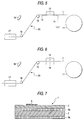
- a plate-making method in which a voltage is applied to both surfaces of an original plate as shown in Fig. 6.
- exposure light emitted from a light source is condensed by a lens 18.
- the condensed exposure light forms an image on a master 1' (lithographic printing original plate) which is fed from a feeder 11 with a transport means and has arrived at an exposure section 20 between guide rollers 15 and 16, thereby effecting imagewise exposure to the master 1'.
- the master 1' Before the master 1' is transported to the exposure section 20, the master 1' is negatively charged on an upper surface of a photoconductive layer 5 by a negative corona discharge means 12 and also positively charged on a lower surface of the photoconductive layer 5 by a positive corona discharge means.
- the water-resistant support which can be used are a paper having been subjected to water-resistant treatment, a metal foil or a composite thereof.
- the electrophotographic method requires some discharge treatment of a plate in conducting corona charging of a photosensitive layer. Where plate-making is conducted by the method as shown in Fig. 6, charging is achieved by bringing the whole support to have conductivity and also conducting positive corona discharge to the support from the back surface thereof.
- the support used is a paper
- conductivity is imparted to the paper by coating it with a solution containing the so-called conductive agent, such as an inorganic electrolyte, e.g., sodium chloride, potassium chloride or calcium chloride, an organic high molecular electrolyte, e.g., a quaternary ammonium salt, or by immersing it in a solution containing such a conductive agent.
- the paper can acquire a volume electric resistance of about 1 ⁇ 10 9 ⁇ cm.
- JP-A a conductive filler-containing water-resistant epoxy resin, ethylene-acrylic acid copolymer, or the like, as described in, e.g., JP-A-50-138904, JP-A-55-105580 and JP-A-59-68753 (The term "JP-A” as used herein means an "unexamined published Japanese patent application"), or attempts to use a conductive resin-laminated paper, such as a paper provided with a conductive filler-containing polyethylene laminate, described in, e.g., JP-A-58-57994 and JP-A-59-64395. In these cases, the paper used is also rendered conductive.
- the lithographic printing plate 1' shown in Fig. 7 is constituted of a support 2 which is prepared by subjecting a paper to a conductive treatment, conductive layers (laminate layers) 3a and 3b provided respectively on the back and front surfaces of the support, and a photoconductive layer 5 provided on the conductive layer 3b. On the photoconductive layer 5, a toner image 6 is formed.
- This conductive resin-laminated paper has a structure that a resin film is provided on one surface or both surfaces of a paper, and the resin film is required to contain a conductive filler. Accordingly, the production cost of such a support is high, and it causes a rise in cost of the lithographic printing plate. Where a paper support is coated with a filler-dispersed resin so as to bring the support to have water resistance, it is unsuccessful to ensure satisfactory physical properties in the coating of resin. Thus, it was difficult to achieve high water resistance and high conductivity at the same time.
- a metal foil-laminated paper a paper to which a metal foil, such as an aluminum, zinc or copper foil, is adhered (hereinafter referred to as "a metal foil-laminated paper") as described in, e.g., JP-B-38-17249, JP-B-41-2426 and JP-B-41-12432 (The term “JP-B” as used herein means an "examined published Japanese patent publication”).
- the paper to be laminated with a metal foil is also a paper soaked with the above-described conductive agent.
- the use of such a metal foil-laminated paper can produce improvements in elongation at wetting and tensile strength, so that it can ensure high dimensional stability in the printing original plate.
- a metal foil-laminated paper As for such a metal foil-laminated paper, it has been attempted to arrange a metal foil on the back surface, on both surfaces or in the center of the paper. In any of such cases, a lithographic printing original plate having excellent dimensional stability can be obtained. However, in any case, a metal foil must be adhered to one or both surfaces of a paper, resulting in increasing production cost of the support as compared with the laminate paper.
- an object of the present invention is to provide a method of producing a lithographic printing plate which is relatively inexpensive, prevents the plate elongation, achieves high-speed processing, and can obtain uniform images.
- the metallic conductive layer provided between the support and the photoconductive layer makes it possible to conduct rapid charging by contacting with a conductor from the side part of the support.
- Examples of a paper used as a support includes conductive original papers conventionally used for electrophotographic photosensitive materials, such as papers impregnated with a conductive substance described hereinbelow, papers into which a conductive substance described hereinbelow is blended in paper-making, and synthetic papers described in JP-B-52-4239, JP-B-53-19031 and JP-B-53-19684. It is preferable for such a paper to have a basis weight of 50 to 200 g/m 2 and a thickness of 50 to 200 ⁇ m.
- Examples of the conductive substance with which a paper can be soaked include solutions containing inorganic electrolytes, such as sodium chloride, potassium chloride and calcium chloride, and solutions containing organic high molecular weight electrolytes, such as quaternary ammonium salts.
- Examples of the conductive substance which can be blended into a paper in paper-making include oxides of metals, such as zinc, magnesium, tin, barium, indium, molybdenum, aluminum, titanium and silicon, and carbon black.
- It is preferable for the support to have a volume electric resistance of 1 ⁇ 10 10 ⁇ cm or below, preferably 1 ⁇ 10 8 ⁇ cm or below, and more preferably 1 ⁇ 10 6 ⁇ cm or below, with the lower limit being generally 1 ⁇ 10 4 ⁇ cm. By controlling the support so as to have such a volume electric resistance, conduction of charges can be secured.
- the metallic conductive layer provided on the support has no particular limitation. Any of simple substances and compounds of metals, such as iron, copper, aluminum, lead and zinc, can be used. Of those, aluminum is especially preferred as a material to be laminated on a paper, because it can be easily formed into a foil due to its low specific gravity and high spreadability. It is preferable for the metallic conductive layer to have a volume electric resistance of 1 ⁇ 10 5 ⁇ cm or below.
- the thickness of the metallic conductive layer is preferably from 5 to 50 ⁇ m, and more preferably from 10 to 25 ⁇ m. Such a metallic conductive layer has a low volume electric resistance, so that it enables the photoconductive layer to be rapidly and uniformly charged.
- the metallic conductive layer can be provided on a support using a conventional means.
- a method of applying an adhesive can be used.
- an adhesive include vinyl acetate resins, acrylic resins, polyolefin resins, urethane resins and phenol resins. These resins are used alone or in the form of mixture or copolymer depending on the end-use purpose.
- the adhesive is emulsified in water to make a water-based paint or dissolved in an appropriate solvent to make a solvent-based paint, and applied to a metal or paper. With the thus applied adhesive, the metallic conductive layer and the support are adhered together.
- Water-soluble resins such as casein and starch, may also be used as an adhesive.
- a hot melt method using a wax resin or a polyolefin resin and an extrusion coating method can be used. It is preferable for the adhesives used to have conductivity. Further, a method of depositing or sputtering a metal onto a support may be used.
- a blocking layer between the metallic conductive layer and the photoconductive layer.
- This blocking layer acts to block the transfer of charges or/and electrons, and therefore has effects to increase a charging efficiency and to inhibit non-uniform charging.
- a resin which can be used for such a blocking layer include polyamide, polyolefin, ethyl acrylate-ethyl methacrylate copolymer, acrylonitrile-methyl methacrylate copolymer, amylose acetate, styrene-butadiene copolymer, polycarbonate, polyvinyl formate, poly-p-chlorostyrene, polyvinyl acetate, polydimethylsiloxane, polystyrene, polyethylacrylate, polyacrylonitrile, polyacenaphthylene, 1,4-polyisoprene, poly-p-isopropylstyrene, polyethylene terephthalate, polyethylene naphthal
- a suitable resin for the blocking layer can be selected.
- polymethyl methacrylate and polyacrylonitrile can be selected because of their high ability to form a uniform film.
- Such a resin is dissolved in an appropriate solvent, and the resulting solution is applied to the metallic conductive layer, and then dried to form a blocking layer.
- such a blocking layer it is preferable for such a blocking layer to have a volume electric resistance of at least 1 ⁇ 10 10 ⁇ cm, and preferably at least 1 ⁇ 10 11 ⁇ cm. Although it is not particularly limited, the upper limit of the volume electric resistance is generally about 1 ⁇ 10 14 ⁇ cm.
- the thickness of a blocking layer is generally from 0.2 to 10 ⁇ m.
- a coating method which can be used herein include a bar coating method, a roll coating method such as gravure or reverse, a doctor knife coating method, an air knife coating method and a nozzle coating method.
- the photoconductive layer used is a layer comprising a binder and zinc oxide (ZnO) dispersed therein.
- the grain size of zinc oxide which can be used is generally about 0.1 to 0.5 ⁇ m.
- the photoconductive layer has no particular limitation on the binder used, and any generally used resins having good mechanical and electric properties can be used as the binder.
- a binder include polystyrene, polyacrylic acid esters, polymethacrylic acid esters, polyvinyl acetate, polyvinyl chloride, polyvinyl butyral, derivatives of the polymers described above, polyester resins, acrylic resins, epoxy resins and silicone resins. Of these resins, acrylic resin is preferred.
- the pigment and such a binder are mixed in a ratio of generally from about 3:1 to about 20:1 by weight.
- the coating build-up of such a photoconductive layer is generally from 15 to 30 g/m 2 .
- the thickness of such a photoconductive layer is preferably from 5 to 30 ⁇ m.
- the laminate layer provided on the other surface of the support comprises an ⁇ -polyolefin.
- ⁇ -polyolefin examples include polyethylene, polypropylene and ethylene-butene copolymer. Of those, polyethylene are preferred. It is preferable to use a polyethylene having a density of 0.92 to 0.96 g/cc, a melt index of 1.0 to 30 g/10 min, an average molecular weight of 20,000 to 50,000, a softening temperature of 110 to 130°C and a tensile strength of 130 to 300 Kg/cm 2 .
- a mixture has heat resistance, can provide a uniform laminate layer, and enables the conductive substance to disperse therein in a state that the electric current easily flows through the conductive substance.
- a conductive substance is incorporated so as to provide the laminate layer having a volume electric resistance of 1 ⁇ 10 10 ⁇ cm or below, preferably 1 ⁇ 10 8 ⁇ cm or below, more preferably 1 ⁇ 10 6 ⁇ cm or below, with lower limit being generally 1 ⁇ 10 2 ⁇ cm.
- a conductive substance which can be used include the same substances as ones blended into the paper support.
- the thickness of the laminate layer is generally about 5 to 50 ⁇ m, and preferably about 10 to 30 ⁇ m.
- a polyethylene derivative such as an ethylene-vinyl acetate copolymer, an ethylene-acrylate copolymer, an ethylene-methacrylate copolymer, an ethylene-acrylic acid copolymer, an ethylene-methacrylic acid copolymer, an ethylene-acrylonitrile-acrylic acid terpolymer and an ethylene-acrylonitrile-methacrylic acid terpolymer, or to previously subject the support surface to a corona discharge treatment.
- a polyethylene derivative such as an ethylene-vinyl acetate copolymer, an ethylene-acrylate copolymer, an ethylene-methacrylate copolymer, an ethylene-acrylic acid copolymer, an ethylene-methacrylic acid copolymer, an ethylene-acrylonitrile-acrylic acid terpolymer and an ethylene-acrylonitrile-methacrylic acid terpolymer, or to previously subject the support surface to a corona discharge treatment.
- the support can undergo the surface treatment as described in, e.g., JP-A-49-24126, JP-A-52-36176, JP-A-52-121683, JP-A-53-2612, JP-A-54-111331 and JP-B-51-25337.
- a backing layer may be provided on the ⁇ -polyolefin containing laminate layer.
- this backing layer are given antislip properties and, if desired, a function as a conductive layer.
- the backing layer has a constitution that the conductive agent and particles for controlling the rigidness (particle size: about 0.1 to 1 ⁇ m) are homogeneously dispersed in a polymer binder.
- Examples of a polymer binder used in the backing layer include polyethylene, polybutadiene, polyacrylate, polymethacrylate, polyamylose acetate, nylon, polycarbonate, polyvinyl formate, polyvinyl acetate, polyacenaphthylene, polyisoprene, polyethylene terephthalate, polyvinyl chloride, polyoxyethylene, polypropylene oxide, polytetrahydrofuran, polyvinyl alcohol, polyphenylene oxide, polypropylene, their copolymers, hardened gelatin, and hardened polyvinyl alcohol.
- the lithographic printing original plate (master) has, on one surface of a paper support 2, a metallic conductive layer 3, a blocking layer 4 and a photoconductive layer 5, which are arranged in that order, and on the other surface of the paper support, a laminate layer 6.
- the photoconductive layer 5 charged by a prescribed operation is exposed to light, forms a toner image thereon by development, and is further oil-desensitized (etched) to provide a lithographic printing plate.
- Fig. 2 is a schematic view showing a process (apparatus) of producing a lithographic printing plate in accordance with the present invention.
- the master 1 is fed from a feeder 11 with a transport means, and arrives at the charging section.
- the photoconductive layer 5 is negatively charged by a negative charging means 12 on the upper side thereof and positively charged by a positive charging means 19 on the lower side thereof.
- a conductor 21 is arranged in front and/or back of the charging means 12 and 19, arranged. The conductor is brought into contact with the side part of the master, and as a result, the metallic conductive layer 3 comes into contact with the conductor.
- the conductor is grounded by an earthing conductor 14, and functions as an earthing electrode when it is brought into contact with the metallic conductive layer 3. Accordingly, it is also possible to use the negative corona discharge means 12 alone. In the thus constituted charging section, it becomes possible to get rid of non-uniform charging and to shorten the charge saturation time. Thus, the processing speed can be increased.
- the conductor 21 can be made of a fibrous or rod-like metallic material having a volume electric resistance of 1 ⁇ 10 3 ⁇ cm or below, such as fibrous or rod-like iron, copper, aluminum and stainless steel which may undergo surface treatment with nickel, chromium or the like, or may be made of carbon fibers or a material prepared by incorporating a conductive substance into a resin and forming the resulting resin into fibers.
- a grounded brush-form or brush-like conductor 21 is arranged in front or/and back of the corona discharge means 12 and 19, and made to approach the master 1 from the side, and thereby comes into direct contact with the metallic conductive layer 3.
- This conductor 21 may have a structure as shown in Fig. 3, wherein a lot of fibrous or rod-like conductors are arranged so as to stand upright on a metal support 23 to be formed into a brush 22, and this brush may be brought into contact with the side part of the master 1.
- parts of the brush 22 stand upright on both sides of the master 1 and come into contact with the metallic conductive layer 3 of the master 1 when the master 1 passes across the brush.
- the charging section By constituting the charging section in this way, the charging can be performed more smoothly, restrictions on the thickness of a support 2 can be removed, the transport speed can be increased, and non-uniform charging can be reduced.
- the photoconductive layer In charging the photoconductive layer, it is also effective to use a method of carrying out negative corona discharge on the surface side of the master 1 and, at the same time, bringing the grounded conductor 13 into contact with the back side of the master 1. More specifically, as shown in Fig. 5, the master 1 is fed from a feeder 11, and arrives at the charging section. In this section, the photoconductive layer 5 is charged negatively on the upper side thereof and positively on the lower side thereof by a negative corona discharge means 12 arranged on the upper side thereof and a conductor 13 which is grounded by an earthing conductor 14 to have earth potential. The conductor 13 is brought into contact with the laminate layer 6 of the master 1, and functions as not only an earthing electrode but also a transport guide.
- the conductor 13 is preferably made of, e.g., a metal such as iron, copper or aluminum, an alloy such as stainless steel, a metal or alloy which has undergone a surface treatment with nickel, chromium or the like, a carbon resin or a material prepared by incorporating a conductive substance into a resin.
- the thickness of the conductor can be properly chosen depending on the property of the material used for making it and the structure of a plate-making apparatus used. As a general guide, the thickness is generally 0.1 to 5 mm. In addition, the size thereof may be chosen depending on the size of a corona discharge means (charger) used and the size of the master 1.
- imagewise exposure is carried out using a laser beam, incandescent light or the like focused by a lens 18.
- the thus exposed master 1 is transported to the development-and-fixation section 17 by a transporting means, developed by attaching toner to the unexposed area, and then subjected to fixation. Further, the thus processed master is subjected to a hydrophilic treatment, and then dried. Thus, an original plate for lithographic printing is produced.
- the toner used is generally a liquid toner.
- Oil-desensitization of zinc oxide can be effected using processing solutions known to be useful for this purpose, such as a processing solution containing as a main component a cyan compound (e.g., ferrocyanide, ferricyanide), a cyan-free processing solution containing as a main component an amine-cobalt complex, phytic acid or a derivative thereof, or a guanidine derivative, a processing solution containing as a main component an inorganic or organic acid capable of forming a chelate together with zinc ion, or a processing solution containing a water-soluble polymer.
- a processing solution containing as a main component a cyan compound e.g., ferrocyanide, ferricyanide
- a cyan-free processing solution containing as a main component an amine-cobalt complex, phytic acid or a derivative thereof, or a guanidine derivative
- Examples of a processing solution containing a cyan compound include those described in, for example, JP-B-44-9045, JP-B-46-39403, JP-A-52-76101, JP-A-57-107889 and JP-A-54-117201.
- Examples of a processing solution containing a phytic acid compound include those described in JP-A-53-83807, JP-A-53-83805, JP-A-53-102102, JP-A-53-109701, JP-A-53-127003, JP-A-54-2803 and JP-A-54-44901.
- Examples of a processing solution containing a metal complex compound such as a cobalt complex include those described in, for example, JP-A-53-104301, JP-A-53-140103, JP-A-54-18304 and JP-B-43-28404.
- Examples of a processing solution containing an inorganic or organic acid include those described in, for example, JP-B-39-13702, JP-B-40-10308, JP-B-43-28408, JP-B-40-26124 and JP-A-51-118501.
- Examples of a processing solution containing a guanidine compound include those described in, for example, JP-A-56-111695.
- Examples of a processing solution containing a water-soluble polymer include those described in, for example, JP-A-52-126302, JP-A-52-134501, JP-A-53-49506, JP-A-53-59502, JP-A-53-104302, JP-B-38-9665, JP-B-39-22263, JP-B-40-763, JP-B-40-2202 and JP-A-49-36402.
- the zinc ion generated by ionization of zinc oxide present in a surface layer undergoes the chelating reaction with a chelating compound contained in the processing solution to form the chelate of zinc ion. It is believed that this chelate is deposited on the surface layer and renders the surface hydrophilic.
- the oil-desensitization is generally carried out for about 0.5 to about 30 seconds at room temperature (15°C-35°C).
- room temperature 15°C-35°C.
- a 5% aqueous solution of calcium chloride was applied to wood free paper at a coating build-up of 20 g/m 2 , and dried to prepare a conductive support having a basis weight of 110 g/m 2 .
- a water-soluble latex of ethylene-methyl acrylate-acrylic acid (65:30:5 by mole) copolymer was coated so as to have a dry coverage of 0.2 g/m 2 , and dried.
- a pellet prepared by melting and kneading a mixture of 70 wt% of a low density polyethylene having a density of 0.920 g/cc and a melt index of 5.0 g/10 min, 15 wt% of a high density polyethylene having a density of 0.950 g/cc and a melt index of 8.0 g/10 min and 15 wt% of carbon black was provided in a thickness of 30 ⁇ m using an extrusion coating method.
- the support and this coating film were adhered together by means of a laminator.
- the thus obtained laminate layer had a volume electric resistance of 7.5 ⁇ 10 6 ⁇ cm.
- the support was coated with a thermosetting conductive adhesive.
- One side of an aluminum foil was coated in advance with an acrylic polymer having a volume electric resistance of 3 ⁇ 10 14 ⁇ cm so as to have a uniform thickness of 2 ⁇ m by means of a wire bar, thereby forming a blocking layer.
- the uncoated side of this aluminum foil and the adhesive-coated side of the support were brought into contact with each other, and allowed to stand for 24 hours at 80°C, thereby adhering them together.
- a metallic conductive layer was formed on the support.
- composition (1) Photoconductive zinc oxide 100 parts by weight Acrylic resin 20 parts by weight Toluene 125 parts by weight Phthalic anhydride 0.1 parts by weight Rose Bengal (4% methanol soln.) 4.5 parts by weight
- the same laminate layer as provided in Sample 1 was provided on the both sides of the same paper support as used for Sample 1.
- the laminate layer provided on one side of the support was subjected to a corona discharge treatment, and provided with the same blocking layer as in Sample 1 without providing with a metallic conductive layer.
- the same photoconductive layer as in Sample 1 was provided, thereby preparing a Comparative Sample.
- each of the thus prepared samples was made into a printing plate using a plate-making apparatus having the constitution as shown in Fig. 2 (ELP-404V, made by Fuji Photo Film Co., Ltd.).
- ELP-404V the conductor 21 as shown in Fig. 3 was arranged in front of chargers 12 and 19 as corona discharge means (the other conductor arranged in back of the chargers was omitted in this case).
- the voltage applied to the negative charger was adjusted to -6 KV
- the voltage applied to the positive charger was adjusted to +6 KV
- the transport speed of each sample was changed from 250 mm/sec to 550 mm/sec at intervals of 50 mm/sec.
- the surface potential of the photoconductive layer, V7 was measured. It is preferable for V7 to be at least 520 V, and more preferably at least 600 V.
- the master prepared in accordance with the present invention was successful in achieving both satisfactory uniformity and V7 greater than 520 V, in the whole range of transport speed, from 250 mm/sec to 550 mm/sec; while the comparative master failed to provide satisfactory uniformity.
- the plate-making was performed in the same manner as in Example 1, except that the conductor was removed from the plate-making apparatus ELP-404V, and the surface potential and the uniformity in the solid area were evaluated using the same criteria. The results obtained are shown in Table 2. (without conductor) Transport speed (mm/sec) Sample 1 Comparative Sample V7 (V) Uniformity V7 (V) Uniformity 250 655 ⁇ 640 ⁇ 300 659 ⁇ 645 ⁇ 350 650 ⁇ 658 ⁇ 400 633 ⁇ 630 X 450 508 ⁇ 520 X 500 445 X 431 X 550 321 X 303 X
- the master prepared in accordance with the present invention although successful in achieving desirable V7 at the transport speed ranging from 250 mm/sec to 400 mm/sec, was unsatisfactory with respect to the uniformity which is reflected in the practical properties; while the comparative master also had the same tendency as the present master, and failed to provide satisfactory uniformity.
- the printing operations were performed using the master obtained above and a printing machine, Oliver 52, made by Sakurai Graphic Systems Co., Ltd., and it was confirmed that the uniformity of printed images corresponded to uniformity of the images formed on the master. Even after printing 10,000 sheets, no elongation was observed at all in the printing plate according to the present invention.
- a lithographic printing plate which can provide uniform images, has neither elongation nor non-uniform charging mark, and can be handled with ease, is produced at low cost.
Landscapes
- Physics & Mathematics (AREA)
- General Physics & Mathematics (AREA)
- Printing Plates And Materials Therefor (AREA)
- Photoreceptors In Electrophotography (AREA)
- Electrostatic Charge, Transfer And Separation In Electrography (AREA)
- Laminated Bodies (AREA)
Applications Claiming Priority (3)
| Application Number | Priority Date | Filing Date | Title |
|---|---|---|---|
| JP4842897 | 1997-02-17 | ||
| JP48428/97 | 1997-02-17 | ||
| JP04842897A JP3217722B2 (ja) | 1997-02-17 | 1997-02-17 | 平版印刷版の製造方法 |
Publications (3)
| Publication Number | Publication Date |
|---|---|
| EP0859287A2 true EP0859287A2 (fr) | 1998-08-19 |
| EP0859287A3 EP0859287A3 (fr) | 1999-06-16 |
| EP0859287B1 EP0859287B1 (fr) | 2003-11-19 |
Family
ID=12803081
Family Applications (1)
| Application Number | Title | Priority Date | Filing Date |
|---|---|---|---|
| EP98102708A Expired - Lifetime EP0859287B1 (fr) | 1997-02-17 | 1998-02-17 | Procédé de fabrication de plaques d'impression lithographiques |
Country Status (4)
| Country | Link |
|---|---|
| US (1) | US5950541A (fr) |
| EP (1) | EP0859287B1 (fr) |
| JP (1) | JP3217722B2 (fr) |
| DE (1) | DE69819794T2 (fr) |
Families Citing this family (3)
| Publication number | Priority date | Publication date | Assignee | Title |
|---|---|---|---|---|
| US6055906A (en) * | 1998-11-04 | 2000-05-02 | Presstek, Inc. | Method of lithographic imaging without defects of electrostatic origin |
| US6544909B1 (en) * | 2000-06-09 | 2003-04-08 | Building Materials Investment Corporation | Single ply reinforced roofing membrane |
| WO2015138667A1 (fr) | 2014-03-12 | 2015-09-17 | 3M Innovative Properties Company | Matériau polymère conducteur |
Family Cites Families (10)
| Publication number | Priority date | Publication date | Assignee | Title |
|---|---|---|---|---|
| DE1196077B (de) * | 1960-07-28 | 1965-07-01 | Eastman Kodak Co | Elektrophotolithographisches Verfahren zur Herstellung von Flachdruckformen |
| US3639121A (en) * | 1969-03-03 | 1972-02-01 | Eastman Kodak Co | Novel conducting lacquers for electrophotographic elements |
| JPS57171356A (en) * | 1981-04-15 | 1982-10-21 | Ricoh Co Ltd | Method and device for recording |
| JPS5824149A (ja) * | 1981-08-06 | 1983-02-14 | Fuji Photo Film Co Ltd | 平版印刷用感光材料 |
| JPS5857994A (ja) * | 1981-10-01 | 1983-04-06 | Fuji Photo Film Co Ltd | 電子写真製版材料 |
| JPS5882791A (ja) * | 1981-11-12 | 1983-05-18 | Ricoh Co Ltd | 平版印刷用原版 |
| JP2561712B2 (ja) * | 1988-06-27 | 1996-12-11 | 富士写真フイルム株式会社 | 電子写真式平版印刷用原版及びその現像方法 |
| JPH0377981A (ja) * | 1989-08-21 | 1991-04-03 | Matsushita Electric Ind Co Ltd | 誘電体層及び誘電体層上の絶縁性粉体層帯電制御方法 |
| US5008167A (en) * | 1989-12-15 | 1991-04-16 | Xerox Corporation | Internal metal oxide filled materials for electrophotographic devices |
| US5382486A (en) * | 1993-03-29 | 1995-01-17 | Xerox Corporation | Electrostatographic imaging member containing conductive polymer layers |
-
1997
- 1997-02-17 JP JP04842897A patent/JP3217722B2/ja not_active Expired - Fee Related
-
1998
- 1998-02-12 US US09/022,459 patent/US5950541A/en not_active Expired - Fee Related
- 1998-02-17 DE DE69819794T patent/DE69819794T2/de not_active Expired - Lifetime
- 1998-02-17 EP EP98102708A patent/EP0859287B1/fr not_active Expired - Lifetime
Also Published As
| Publication number | Publication date |
|---|---|
| EP0859287A3 (fr) | 1999-06-16 |
| DE69819794T2 (de) | 2004-08-19 |
| JP3217722B2 (ja) | 2001-10-15 |
| US5950541A (en) | 1999-09-14 |
| EP0859287B1 (fr) | 2003-11-19 |
| DE69819794D1 (de) | 2003-12-24 |
| JPH10228136A (ja) | 1998-08-25 |
Similar Documents
| Publication | Publication Date | Title |
|---|---|---|
| US4508804A (en) | Support for electrographic plate-making material and a lithographic printing plate employing same | |
| EP0266466A2 (fr) | Procédé pour élaborer un masque à haute résolution à la surface d'un conducteur et toner liquide utilisé dans ce procédé | |
| EP0349249B1 (fr) | Produit de départ pour plaque d'impression lithographique, électrophotographique et procédé pour son développement | |
| JPH0147785B2 (fr) | ||
| EP0859287B1 (fr) | Procédé de fabrication de plaques d'impression lithographiques | |
| US4555461A (en) | Process for preparing a lithographic printing plate | |
| JP2561713B2 (ja) | 電子写真式平版印刷用原版及びその現像方法 | |
| US6022654A (en) | Production process of lithographic printing plate | |
| EP0546195B1 (fr) | Plaque d'impression pour lithographie electrophotographique | |
| CA1090408A (fr) | Methode et fabrication de matrices et/ou d'images metallisees | |
| US6207332B1 (en) | Process for producing lithographic printing plate | |
| US4500618A (en) | Electrophotographic process for producing printing plate and plate making machine | |
| US3581661A (en) | Electrostatically imaged lithographic plate | |
| US3492206A (en) | Printing method utilizing electrolysis | |
| JPH0157910B2 (fr) | ||
| JP3807244B2 (ja) | 電子写真式平版印刷版用支持体 | |
| JPH11143136A (ja) | 平版印刷版の製造方法および平版印刷版製造用シート | |
| JP3633948B2 (ja) | 電子写真式平版印刷版 | |
| GB2131966A (en) | Manufacture of transfer materials | |
| JPH0445823B2 (fr) | ||
| JP2561713C (fr) | ||
| JPH02127656A (ja) | 電子写真複写用に好適なフィルム | |
| JPS61152489A (ja) | 電子写真平版印刷版 | |
| JPS61152492A (ja) | 電子写真平版印刷版 | |
| JPH10282734A (ja) | 電子写真式直描型平版印刷版 |
Legal Events
| Date | Code | Title | Description |
|---|---|---|---|
| PUAI | Public reference made under article 153(3) epc to a published international application that has entered the european phase |
Free format text: ORIGINAL CODE: 0009012 |
|
| AK | Designated contracting states |
Kind code of ref document: A2 Designated state(s): DE FR GB |
|
| AX | Request for extension of the european patent |
Free format text: AL;LT;LV;MK;RO;SI |
|
| PUAL | Search report despatched |
Free format text: ORIGINAL CODE: 0009013 |
|
| AK | Designated contracting states |
Kind code of ref document: A3 Designated state(s): AT BE CH DE DK ES FI FR GB GR IE IT LI LU MC NL PT SE |
|
| AX | Request for extension of the european patent |
Free format text: AL;LT;LV;MK;RO;SI |
|
| RIC1 | Information provided on ipc code assigned before grant |
Free format text: 6G 03G 13/00 A, 6G 03G 13/28 B, 6G 03G 13/02 B |
|
| 17P | Request for examination filed |
Effective date: 19991201 |
|
| AKX | Designation fees paid |
Free format text: DE FR GB |
|
| GRAH | Despatch of communication of intention to grant a patent |
Free format text: ORIGINAL CODE: EPIDOS IGRA |
|
| GRAS | Grant fee paid |
Free format text: ORIGINAL CODE: EPIDOSNIGR3 |
|
| GRAA | (expected) grant |
Free format text: ORIGINAL CODE: 0009210 |
|
| AK | Designated contracting states |
Kind code of ref document: B1 Designated state(s): DE FR GB |
|
| REG | Reference to a national code |
Ref country code: GB Ref legal event code: FG4D |
|
| REF | Corresponds to: |
Ref document number: 69819794 Country of ref document: DE Date of ref document: 20031224 Kind code of ref document: P |
|
| ET | Fr: translation filed | ||
| PLBE | No opposition filed within time limit |
Free format text: ORIGINAL CODE: 0009261 |
|
| STAA | Information on the status of an ep patent application or granted ep patent |
Free format text: STATUS: NO OPPOSITION FILED WITHIN TIME LIMIT |
|
| 26N | No opposition filed |
Effective date: 20040820 |
|
| REG | Reference to a national code |
Ref country code: FR Ref legal event code: TP Ref country code: FR Ref legal event code: CD |
|
| REG | Reference to a national code |
Ref country code: GB Ref legal event code: 732E Free format text: REGISTERED BETWEEN 20100401 AND 20100407 |
|
| PGFP | Annual fee paid to national office [announced via postgrant information from national office to epo] |
Ref country code: FR Payment date: 20100223 Year of fee payment: 13 |
|
| PGFP | Annual fee paid to national office [announced via postgrant information from national office to epo] |
Ref country code: GB Payment date: 20100202 Year of fee payment: 13 Ref country code: DE Payment date: 20100226 Year of fee payment: 13 |
|
| REG | Reference to a national code |
Ref country code: FR Ref legal event code: TP |
|
| GBPC | Gb: european patent ceased through non-payment of renewal fee |
Effective date: 20110217 |
|
| REG | Reference to a national code |
Ref country code: FR Ref legal event code: ST Effective date: 20111102 |
|
| REG | Reference to a national code |
Ref country code: DE Ref legal event code: R119 Ref document number: 69819794 Country of ref document: DE Effective date: 20110901 |
|
| PG25 | Lapsed in a contracting state [announced via postgrant information from national office to epo] |
Ref country code: FR Free format text: LAPSE BECAUSE OF NON-PAYMENT OF DUE FEES Effective date: 20110228 |
|
| PG25 | Lapsed in a contracting state [announced via postgrant information from national office to epo] |
Ref country code: GB Free format text: LAPSE BECAUSE OF NON-PAYMENT OF DUE FEES Effective date: 20110217 |
|
| PG25 | Lapsed in a contracting state [announced via postgrant information from national office to epo] |
Ref country code: DE Free format text: LAPSE BECAUSE OF NON-PAYMENT OF DUE FEES Effective date: 20110901 |