EP0859461A1 - Circuit mélangeur à étendue dynamique élevée - Google Patents
Circuit mélangeur à étendue dynamique élevée Download PDFInfo
- Publication number
- EP0859461A1 EP0859461A1 EP97102593A EP97102593A EP0859461A1 EP 0859461 A1 EP0859461 A1 EP 0859461A1 EP 97102593 A EP97102593 A EP 97102593A EP 97102593 A EP97102593 A EP 97102593A EP 0859461 A1 EP0859461 A1 EP 0859461A1
- Authority
- EP
- European Patent Office
- Prior art keywords
- transistor
- type differential
- mixer circuit
- unbalance
- circuit
- Prior art date
- Legal status (The legal status is an assumption and is not a legal conclusion. Google has not performed a legal analysis and makes no representation as to the accuracy of the status listed.)
- Withdrawn
Links
- 230000009977 dual effect Effects 0.000 claims description 7
- 230000003139 buffering effect Effects 0.000 claims description 3
- 239000000872 buffer Substances 0.000 abstract 1
- 238000010586 diagram Methods 0.000 description 24
- 238000004088 simulation Methods 0.000 description 12
- 235000013599 spices Nutrition 0.000 description 6
- 238000006243 chemical reaction Methods 0.000 description 2
- 239000003990 capacitor Substances 0.000 description 1
- 230000000295 complement effect Effects 0.000 description 1
- 230000000694 effects Effects 0.000 description 1
Images


Classifications
-
- H—ELECTRICITY
- H03—ELECTRONIC CIRCUITRY
- H03F—AMPLIFIERS
- H03F1/00—Details of amplifiers with only discharge tubes, only semiconductor devices or only unspecified devices as amplifying elements
- H03F1/32—Modifications of amplifiers to reduce non-linear distortion
- H03F1/3211—Modifications of amplifiers to reduce non-linear distortion in differential amplifiers
-
- H—ELECTRICITY
- H03—ELECTRONIC CIRCUITRY
- H03D—DEMODULATION OR TRANSFERENCE OF MODULATION FROM ONE CARRIER TO ANOTHER
- H03D7/00—Transference of modulation from one carrier to another, e.g. frequency-changing
- H03D7/14—Balanced arrangements
- H03D7/1425—Balanced arrangements with transistors
- H03D7/1433—Balanced arrangements with transistors using bipolar transistors
-
- H—ELECTRICITY
- H03—ELECTRONIC CIRCUITRY
- H03D—DEMODULATION OR TRANSFERENCE OF MODULATION FROM ONE CARRIER TO ANOTHER
- H03D7/00—Transference of modulation from one carrier to another, e.g. frequency-changing
- H03D7/14—Balanced arrangements
- H03D7/1425—Balanced arrangements with transistors
- H03D7/1441—Balanced arrangements with transistors using field-effect transistors
-
- H—ELECTRICITY
- H03—ELECTRONIC CIRCUITRY
- H03D—DEMODULATION OR TRANSFERENCE OF MODULATION FROM ONE CARRIER TO ANOTHER
- H03D7/00—Transference of modulation from one carrier to another, e.g. frequency-changing
- H03D7/14—Balanced arrangements
- H03D7/1425—Balanced arrangements with transistors
- H03D7/1458—Double balanced arrangements, i.e. where both input signals are differential
-
- H—ELECTRICITY
- H03—ELECTRONIC CIRCUITRY
- H03D—DEMODULATION OR TRANSFERENCE OF MODULATION FROM ONE CARRIER TO ANOTHER
- H03D7/00—Transference of modulation from one carrier to another, e.g. frequency-changing
- H03D7/14—Balanced arrangements
- H03D7/1425—Balanced arrangements with transistors
- H03D7/1491—Arrangements to linearise a transconductance stage of a mixer arrangement
-
- H—ELECTRICITY
- H03—ELECTRONIC CIRCUITRY
- H03F—AMPLIFIERS
- H03F2203/00—Indexing scheme relating to amplifiers with only discharge tubes or only semiconductor devices as amplifying elements covered by H03F3/00
- H03F2203/45—Indexing scheme relating to differential amplifiers
- H03F2203/45198—A parallel resonance circuit being added in the one or more load circuits of the dif amp
Definitions
- the present invention relates to a mixer circuit, and more particularly to a mixer circuit which is used for a communication equipment.
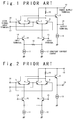
- FIG. 1 is a circuit diagram illustrating the first conventional example of the mixer circuit composed of a dual differential circuit which is composed of transistors 5 to 8, 25 and 26.
- an input signal is inputted between input terminals 14 and 15 and are mixed with a local signal which is inputted between local signal input terminals 16 and 17.
- the mixed signal is outputted to an output terminal 18 as an output signal.
- a resistor 30 is inserted between the emitters of the transistors 25 and 26 for making wide the dynamic range of a differential circuit composed of the transistors 25 and 26.
- the thermal noise generated from the resistor 30 is one of causes that the noise performance is degraded.
- Fig. 2 is a circuit diagram illustrating the second conventional example of the mixer circuit.
- the difference point in structure between the second conventional example shown in Fig. 2 and the first conventional example shown in Fig. 1 is in that the resistor 30 is removed.
- the resistor 30 is removed.
- the dynamic range of the differential circuit of an input section which is composed of the transistors 25 and 26 is made narrow.
- the noise performance becomes better than the mixer circuit of the first convention example shown in Fig. 1.
- Fig. 3 is a circuit diagram of the differential circuit extracted from the second conventional example of the mixer circuit shown in Fig. 2 and the differential circuit of the input section for the input signal is composed of the transistors 25 and 26.
- the present invention is made in the light of the above-mentioned circumstances.
- An object of the present invention is to provide a mixer circuit in which noise performance can be improved and an input dynamic range can be made wide.
- a mixer circuit includes a first unbalance type differential circuit having a first unbalance current ratio, wherein the first unbalance type differential circuit is connected to first output terminals and first input terminals, an input signal being inputted between the first input terminals; a second unbalance type differential circuit having a second unbalance current ratio inverse to the first unbalance current ratio of the first unbalance type differential circuit, wherein the second unbalance type differential circuit is connected to the first output terminals and the first input terminals in parallel to the first unbalance type differential circuit; a first balance type differential circuit connected to one of the first output terminals, connected to one of second output terminals, and connected to second input terminals such that a local signal is supplied to the first balance type differential circuit in a first connection manner; a second balance type differential circuit connected to the other of the first output terminals, connected to the other of the second output terminals, and connected to the second input terminals such that the local signal is supplied to the second balance type differential circuit in a
- the first unbalance current ratio is in a range of 4 to 8, and the most preferable that the unbalance current ratio is 6.
- the first unbalance type differential circuit is composed of first and second transistors connected to the first input terminals and the first output terminals, and having emitters connected in common, respectively.
- the second unbalance type differential circuit is composed of third and fourth transistors connected to the first input terminals and the first output terminals, and having emitters connected in common, respectively.
- the first and second transistors flow current in accordance with the first unbalance current ratio in the first unbalance type differential circuit.
- the third and fourth transistors flow current in accordance the second unbalance current ratio in the second unbalance type differential circuit.
- the first transistor may have an emitter area wider than the second transistor in proportional to the first unbalance current ratio and the fourth transistor may have an emitter area wider than the third transistor in proportional to the second unbalance current ratio.
- n transistors each having the same emitter area as the second transistor and connected in parallel may be used in place of the first transistor and n transistors each having the same emitter area as the third transistor and connected in parallel may be used in place of the fourth transistor.
- the load circuit When the converting section is composed of a load circuit connected to one of the first output terminals of the first and second balance type differential circuits, the load circuit may be composed of a resistor, or the load circuit may be a resonance circuit.
- a mixer circuit includes a first transistor whose base is connected to one of first input terminals for a first input signal, a second transistor whose base is connected to the one of the first input terminals and whose collector is connected to a first common node together with a collector of the first transistor, a third transistor whose base is connected to the other of the first input terminals, and whose emitter is connected to a first current source together with an emitter of the first transistor, wherein the first transistor can flow current n times (n is a positive value in a range of 4 to 8) more than the third transistor such that the first and third transistors form a first unbalance type differential circuit, a fourth transistor whose base is connected to the other of the first input terminals, whose collector is connected to a second common node together with a collector of the third transistor, and whose emitter is connected to a second current source together with an emitter of the second transistor, wherein the fourth transistor can flow current n times more than the second transistor such that
- a mixer circuit using a dual differential circuit comprising an input section includes a first transistor whose base is connected to a first input terminal for a first input signal, a second transistor whose base is connected to the first input terminal and whose collector is connected to a first common node together with a collector of the first transistor, a third transistor whose base is connected to a second input terminal for a second input signal, and whose emitter is connected to a first current source together with an emitter of the first transistor, wherein the first transistor can flow current n times (n is a positive value in a range of 4 to 8) more than the third transistor such that the first and third transistors form a first unbalance type differential circuit, and a fourth transistor whose base is connected to the second input terminal, whose collector is connected to a second common node together with a collector of the third transistor, and whose emitter is connected to a second current source together with an emitter of the second transistor, wherein the fourth transistor can flow current n
- Fig. 5 is a circuit diagram of the mixer circuit according to the first embodiment of the present invention.
- the mixer circuit includes an input section for an input signal composed of the first unbalance type differential circuit and the second unbalanced differential circuit.
- the first unbalance type differential circuit is composed of NPN transistors 1 and 3 whose emitters are connected in common to a constant current source 11.
- An input signal is supplied to the bases of the transistors 1 and 3.
- the emitter area of the transistor 1 is wide n times (n is a positive number), compared to that of the transistor 3.
- the transistor 1 can flow collector current n times more than the transistor 3.
- the second unbalance type differential circuit is composed of NPN transistors 2 and 4 whose emitters are connected in common to a constant current source 12.
- the input signal is also supplied to the bases of the transistors 2 and 4.
- the emitter area of the transistor 4 is wide n times, compared to that of the transistor 2.
- the transistor 4 can flow more collector current n times than the transistor 2.
- the collectors of the transistors 1 and 2 are connected to a common node 41 in common and the collectors of the transistors 3 and 4 are connected to a common node 42 in common.
- the constant current source 11 flows current of the same magnitude as the constant current source 12.
- the mixer circuit of the first embodiment is composed of the first and second local balance type differential circuits.
- the first local balance type differential circuit is composed of NPN transistors 5 and 6 and the second local balance type differential circuit is composed of NPN transistors 7 and 8.
- the bases of the transistors 5 and 8 are connected in common to a local signal input terminal 16 and the bases of the transistors 6 and 7 are connected in common to a local signal input terminal 17. That is, the local signal is supplied to the second balance type differential circuit in a connection manner inverse to that in the first balance type differential circuit.
- the emitters of the transistors 5 and 6 are connected in common to the common node 41 to which the collectors of the transistors 1 and 2 are connected in common.
- the emitters of the transistors 7 and 8 are connected to the common node 42 to which the collectors of the transistors 3 and 4 are connected in common.
- the collectors of the transistors 5 and 7 are connected in common to a power supply terminal 19 via a common node 43.
- the collectors of the transistors 6 and 8 are connected to a common node 44 in common.
- a resistor 10 is provided between the power supply terminal 19 and the common node 44.
- the common node 44 between the resistor 10 and the collector of the transistor 8 is connected to the base of an NPN transistor 9 of an output section.
- the collector of the transistor 9 is connected to the power supply terminal 19.
- the output section is further composed of a constant current source 13 and the emitter of the transistor 9 is connected to the constant current source 13.
- An output of the mixer circuit in the first embodiment is taken out from an output terminal 18 between the emitter of the transistor 9 and the constant current source 13.
- the current value of the constant current source 13 is determined based on impedance conversion.
- the mixer circuit in the first embodiment is different from the conventional examples at the following point. That is, the balance type differential circuit composed of the transistors 25 and 26 in the conventional examples is replaced by parallel connection of the unbalance type differential circuit composed of the transistors 1 and 3 and the unbalance type differential circuit composed of the transistors 2 and 4.
- Fig. 6 is a circuit diagram illustrating the input section which is extracted from the mixer circuit shown in Fig. 5.
- Fig. 7 is a characteristic diagram illustrating the simulation result of the input section shown in Fig. 6 by the simulation apparatus SPICE.
- the input section of the first embodiment is composed of the unbalance type differential circuit composed of the transistors 1 and 3 and the unbalance type differential circuit composed of the transistors 2 and 4.
- a variable voltage supply 28 is connected between the bases of the transistors 1 and 2 and the bases of the transistors 3 and 4.
- Both of the constant current source 11 and 12 flow the current of 0.5 mA.
- the current I and the voltage ⁇ V are simulated by the simulation apparatus SPICE.
- the dynamic range of the input section is simulated while n is changed, where n is an emitter area factor.
- Fig. 7 is a characteristic diagram illustrating the simulation result of the dynamic range of the input section by the simulation apparatus SPICE when n is 6.
- the value of n may be changed in accordance with the required dynamic range. That is, these unbalance type differential circuits complement the dynamic range with each other to make the total dynamic range wide.
- Fig. 8 is the circuit diagram illustrating the mixer circuit according to the second embodiment of the present invention.
- the mixer circuit of the second embodiment has substantially the same circuit structure as that of the first embodiment.
- the mixer circuit of the second embodiment is different from that of the first embodiment in the point that a resistor 20 having the same resistance as the resistor 10 is inserted between the power supply terminal 19 and the common node 43 between the collectors of the transistors 5 and 7 and the output is taken out in the differential form.
- the output section is further composed of a constant current source 29 and a transistor 21 whose collector is connected to the power supply terminal 19, whose base is connected to the common node 43 between the resistor 20 and the collectors of the transistors 5 and 7, and whose emitter is connected to the constant current source 29 which supplies the same current as the constant current source 13, in addition to the transistor 9 and the constant current source 13.
- the output is supplied in a differential manner by the output terminal 18 and the output terminal 22 between the emitter of the transistor 21 and the constant current source 29. In this case, it has the advantage that the gain can be obtained twice.
- Fig. 9 is the circuit diagram illustrating the mixer circuit according to the third embodiment of the present invention.
- the mixer circuit of the third embodiment has substantially the same circuit structure as that of the first embodiment.
- the mixer circuit of the third embodiment is different from that of the first embodiment in the point that a resistor 10 as load is replaced by a parallel resonance circuit which is composed of a capacitor 23, the resistor 10, and an inductor 24.
- band limitation can be performed to the output signal in the band by the parallel resonance circuit, there is the advantage that noise and spurious output can be suppressed.
- Fig. 10 is the circuit diagram illustrating the mixer circuit according to the fourth embodiment of the present invention.
- the mixer circuit of the fourth embodiment has substantially the same circuit structure as that of the first embodiment.
- the mixer circuit of the fourth embodiment is different from that of the first embodiment in the point that n NPN transistors 1-1, ..., 1-n each of which has the same characteristics as the transistor 3 is used in place of the transistor 1 and n NPN transistors 4-1, ..., 4-n each of which has the same characteristics as the transistor 2 is used in place of the transistor 4.
- the NPN transistors are used.
- N-channel MOS transistors could be applied in place of the NPN transistors. If the circuit diagram is rewritten, PNP transistors or P-channel MOS transistors could be also applied.
- the unbalance type differential circuits are connected in parallel for the input section of the input signal in the dual differential circuits instead of the balance type differential circuit, there is achieved the effect that the noise performance is good and moreover that the dynamic range of the differential circuit in the input section is wide.
Landscapes
- Engineering & Computer Science (AREA)
- Power Engineering (AREA)
- Physics & Mathematics (AREA)
- Nonlinear Science (AREA)
- Amplifiers (AREA)
Priority Applications (1)
| Application Number | Priority Date | Filing Date | Title |
|---|---|---|---|
| EP97102593A EP0859461A1 (fr) | 1997-02-18 | 1997-02-18 | Circuit mélangeur à étendue dynamique élevée |
Applications Claiming Priority (1)
| Application Number | Priority Date | Filing Date | Title |
|---|---|---|---|
| EP97102593A EP0859461A1 (fr) | 1997-02-18 | 1997-02-18 | Circuit mélangeur à étendue dynamique élevée |
Publications (1)
| Publication Number | Publication Date |
|---|---|
| EP0859461A1 true EP0859461A1 (fr) | 1998-08-19 |
Family
ID=8226490
Family Applications (1)
| Application Number | Title | Priority Date | Filing Date |
|---|---|---|---|
| EP97102593A Withdrawn EP0859461A1 (fr) | 1997-02-18 | 1997-02-18 | Circuit mélangeur à étendue dynamique élevée |
Country Status (1)
| Country | Link |
|---|---|
| EP (1) | EP0859461A1 (fr) |
Cited By (1)
| Publication number | Priority date | Publication date | Assignee | Title |
|---|---|---|---|---|
| FR2836305A1 (fr) * | 2002-02-15 | 2003-08-22 | St Microelectronics Sa | Melangeur differentiel classe ab |
Citations (4)
| Publication number | Priority date | Publication date | Assignee | Title |
|---|---|---|---|---|
| GB2064253A (en) * | 1979-11-23 | 1981-06-10 | Philips Nv | Controllable-gain mixer circuit |
| EP0501827A2 (fr) * | 1991-03-01 | 1992-09-02 | Kabushiki Kaisha Toshiba | Circuit multiplicateur |
| GB2260870A (en) * | 1991-10-25 | 1993-04-28 | Nec Corp | Frequency mixers |
| GB2284116A (en) * | 1993-10-27 | 1995-05-24 | Nec Corp | Mixing circuits |
-
1997
- 1997-02-18 EP EP97102593A patent/EP0859461A1/fr not_active Withdrawn
Patent Citations (4)
| Publication number | Priority date | Publication date | Assignee | Title |
|---|---|---|---|---|
| GB2064253A (en) * | 1979-11-23 | 1981-06-10 | Philips Nv | Controllable-gain mixer circuit |
| EP0501827A2 (fr) * | 1991-03-01 | 1992-09-02 | Kabushiki Kaisha Toshiba | Circuit multiplicateur |
| GB2260870A (en) * | 1991-10-25 | 1993-04-28 | Nec Corp | Frequency mixers |
| GB2284116A (en) * | 1993-10-27 | 1995-05-24 | Nec Corp | Mixing circuits |
Cited By (2)
| Publication number | Priority date | Publication date | Assignee | Title |
|---|---|---|---|---|
| FR2836305A1 (fr) * | 2002-02-15 | 2003-08-22 | St Microelectronics Sa | Melangeur differentiel classe ab |
| US6882194B2 (en) | 2002-02-15 | 2005-04-19 | Stmicroelectronics S.A. | Class AB differential mixer |
Similar Documents
| Publication | Publication Date | Title |
|---|---|---|
| US5929710A (en) | Cascode single-ended to differential converter | |
| US5121080A (en) | Amplifier with controlled output impedance | |
| CA2289212C (fr) | Dephaseur multiple actif | |
| EP0500694A1 (fr) | Amplificateur de puissance cmos entierement differentiel. | |
| US6242963B1 (en) | Differential mixer with improved linearity | |
| KR940004925A (ko) | 트랜스포머 회로 및 이중 평형 믹서 회로 | |
| JPH0452645B2 (fr) | ||
| US6138000A (en) | Low voltage temperature and Vcc compensated RF mixer | |
| EP0696847B1 (fr) | Circuit convertisseur tension-courant pouvant être alimenté par une tension d'alimentation basse | |
| US5357188A (en) | Current mirror circuit operable with a low power supply voltage | |
| KR100526642B1 (ko) | 저항기네트워크에의해공통모드전압거절을가진싱글엔드형신호로차동신호를변환하기위한전자회로 | |
| US5463309A (en) | Variable voltage to current conversion circuit | |
| US20040066232A1 (en) | Variable-gain differential input and output amplifier | |
| EP0499263A1 (fr) | Circuit amplificateur RF | |
| JPH0969730A (ja) | 周波数ミキサ回路 | |
| US5973539A (en) | Mixer circuit for mixing two signals having mutually different frequencies | |
| US6661286B2 (en) | Variable gain amplifier | |
| WO2002082642A2 (fr) | Polarisation dynamique d'emetteur | |
| GB2147754A (en) | Frequency multiplying circuit | |
| US7274256B2 (en) | Input amplifier stage in the AB class having a controlled bias current | |
| AU750998B2 (en) | Electric-field strength detection circuit | |
| EP0859460B1 (fr) | Circuit mélangeur à gamme dynamique étendue | |
| JPH06204762A (ja) | 演算増幅器及びその駆動方法 | |
| JPH04208702A (ja) | 周波数変換回路 | |
| JP3544950B2 (ja) | 可変利得増幅回路 |
Legal Events
| Date | Code | Title | Description |
|---|---|---|---|
| PUAI | Public reference made under article 153(3) epc to a published international application that has entered the european phase |
Free format text: ORIGINAL CODE: 0009012 |
|
| AK | Designated contracting states |
Kind code of ref document: A1 Designated state(s): DE GB |
|
| 17P | Request for examination filed |
Effective date: 19980918 |
|
| AKX | Designation fees paid |
Free format text: DE GB |
|
| RBV | Designated contracting states (corrected) |
Designated state(s): DE GB |
|
| STAA | Information on the status of an ep patent application or granted ep patent |
Free format text: STATUS: THE APPLICATION HAS BEEN WITHDRAWN |
|
| 18W | Application withdrawn |
Withdrawal date: 19990614 |