EP0859494A2 - Synchronisation de l'oscillateur local, dans des systèmes multiporteurs - Google Patents
Synchronisation de l'oscillateur local, dans des systèmes multiporteurs Download PDFInfo
- Publication number
- EP0859494A2 EP0859494A2 EP98102595A EP98102595A EP0859494A2 EP 0859494 A2 EP0859494 A2 EP 0859494A2 EP 98102595 A EP98102595 A EP 98102595A EP 98102595 A EP98102595 A EP 98102595A EP 0859494 A2 EP0859494 A2 EP 0859494A2
- Authority
- EP
- European Patent Office
- Prior art keywords
- complex
- ofdm
- reference symbol
- signal
- vector
- Prior art date
- Legal status (The legal status is an assumption and is not a legal conclusion. Google has not performed a legal analysis and makes no representation as to the accuracy of the status listed.)
- Withdrawn
Links
Images


Classifications
-
- H—ELECTRICITY
- H04—ELECTRIC COMMUNICATION TECHNIQUE
- H04L—TRANSMISSION OF DIGITAL INFORMATION, e.g. TELEGRAPHIC COMMUNICATION
- H04L27/00—Modulated-carrier systems
- H04L27/26—Systems using multi-frequency codes
- H04L27/2601—Multicarrier modulation systems
- H04L27/2647—Arrangements specific to the receiver only
- H04L27/2655—Synchronisation arrangements
- H04L27/2657—Carrier synchronisation
-
- H—ELECTRICITY
- H04—ELECTRIC COMMUNICATION TECHNIQUE
- H04L—TRANSMISSION OF DIGITAL INFORMATION, e.g. TELEGRAPHIC COMMUNICATION
- H04L27/00—Modulated-carrier systems
- H04L27/26—Systems using multi-frequency codes
- H04L27/2601—Multicarrier modulation systems
- H04L27/2647—Arrangements specific to the receiver only
- H04L27/2655—Synchronisation arrangements
- H04L27/2668—Details of algorithms
- H04L27/2673—Details of algorithms characterised by synchronisation parameters
- H04L27/2675—Pilot or known symbols
Definitions
- the present invention relates to an Orthogonal Frequency Division Multiplex (OFDM) Transmission System exchanging an OFDM signals between a transmission side and a receiving side and, more particularly, to a phase compensation as well as a frequency synchronization of a frequency oscillator used therein.
- OFDM Orthogonal Frequency Division Multiplex
- OFDM Orthogonal Frequency Division Muitiplexing
- an original complex data is assigned to a lots of sub-carriers orthogonal to each other on a frequency axis. These assigned complex data are applied with the Fourier transformation to convert themselves into an OFDM signal that is a digital signal modulated in time domain. Thus generated OFDM signal is transmitted to the receiving station.
- the OFDM signal from the transmitting station is applied with the processes substantially the same as those, but in a reversed order, applied on the transmitting station.
- the original complex data is reproduced from the OFDM signal. Since each modulated data assigned to sub-carrier have longer periods, the OFDM signal is well proof against bad influences due to superposition of signals having waves delayed from the direct wave in multi-paths.
- the conventional OFDM signal transmission system is constructed by an OFDM modulation apparatus MC used on a transmission side for modulating an original complex data into the generating an OFDM signal, and an OFDM demodulation apparatus DC used on a receiving side for demodulating the OFDM signal to the original complex data.
- the conventional OFDM modulation apparatus MC includes an input terminal Pim, an inverse Fourier transformer 91, a quadrature modulator 92, a local oscillator 93, and an output terminal Pom.
- the local oscillator 93 generates a local oscillating signal So.
- the input terminal Pim is connected a complex data source externally provided (not shown in Fig. 12) for receiving the original complex data Vms therefrom.
- the inverse Fourier transformer 91 is connected to the input terminal Pim for receiving the original complex data Vms therefrom.
- the inverse Fourier transformer 91 assigns the original complex data Vms, by every symbol included therein, to plural sub-carriers orthogonal to each other on the frequency axis.
- the inverse Fourier transformer 91 applies the inverse Fourier transformation process to those assigned modulated vector signals Vms which are signals in frequency domain to convert into signals in time domain, and generates a base band OFDM signal Vmr.
- the quadrature modulator 92 is connected to the inverse Fourier transformer 91 and the local oscillator 93 for receiving the base band OFDM signal Vmr and the local oscillating signal So, respectively, therefrom. Based on the oscillating signal So, the quadrature modulator 92 performs the orthogonal transformation of the base band OFDM signal Vmr, and then a frequency of the orthogonal transformed base band OFDM signal Vmr is converted to generate an OFDM (orthogonal frequency division multiplexed) signal Vmo having frequency in a middle frequency range or a radio frequency range.
- the output terminal Pom is connected to the quadrature modulator 92 for receiving the OFDM signal Vmo therefrom to supply thereof to the transmitter of the transmission station (not shown in Fig. 12).
- the OFDM demodulating apparatus DC used for demodulating the OFDM signal Vmo generated by the OFDM modulating apparatus MC is shown.
- the OFDM demodulating apparatus DC includes an input terminal Pid, an quadrature detector 101, a Fourier transformer 102, a demodulated data analyzer 103, a frequency controller 104, a local oscillator 105, and an output terminal Pod.
- the local oscillator 105 generates a local oscillating signal So'.
- the local oscillating signal So' has a frequency similar to, but is not the same as that of the signal So generated by the oscillator 93 of the OFDM modulating apparatus MC (Fig. 12). This frequency difference between two local oscillating signals essentially comes from the variation of quartz crystals each used therein.
- the input terminal Pid is connected a receiver of the receiving station (not shown in Fig. 13) for receiving the OFDM signal Vmo therefrom.
- the quadrature detector 101 is connected to the input terminal Pid and the local oscillator 105 for receiving the OFDM signal Vmo and the local oscillating signal So' therefrom, respectively.
- the quadrature detector 101 performs the orthogonal detection of OFDM signal Vmo based on the local oscillating signal So' to generate a base-band OFDM signal Vmb.
- the Fourier Transformer 102 is connected to the quadrature detector 101 for receiving the base-band OFDM signal Vmb therefrom.
- the Fourier Transformer 102 applies a Fourier Transforming to the OFDM signal Vmb by every symbol therein to generate a complex detection signal Vmd which will be output therefrom as the original complex data Vms demodulated from the OFDM signal Vmo.
- the output terminal Pod and the demodulated data analyzer 103 are connected to the Fourier Transformer 102 for receiving the demodulated complex signal Vmd therefrom.
- the demodulated complex data Vmd is not the same as the original complex data Vms with respect to the frequency. This difference in frequency disables the reproduction of the information included in the original complex data Vms from the demodulated complex data Vmd.
- the demodulated complex data Vmd is transferred outward through the output terminal Pod.
- the demodulated data analyzer 103 extracts a demodulated vector from the demodulated complex data Vmd over more than two different sub-carriers, and obtains a frequency error of the local oscillating signal So' for the orthogonal detection based on that phase shift of thus obtained demodulated complex data Vmd to generate a frequency error signal Sfe.
- This process utilizes the phenomena that the phase sift angle of the demodulated complex data, converted from the OFDM signal Vmo by the Fourier transformer 102, can be determined by the error of frequency detection, and that the frequency of sub-carrier contributes to the phase shift angle of demodulated complex data Vmd caused by the frequency detection error. Since the demodulated complex data Vmd also contains the phase shift peculiar to the modulation process itself, the demodulated data analyzer 103 detects the phase shift angle by superimposing the demodulated complex data Vmd over plural symbols.
- the frequency controller 104 is connected to the demodulated data analyzer 103 for receiving the frequency error signal Sfe to generate a frequency control signal Sfc.
- the local oscillator 105 is connected to the frequency controller therefrom for receiving the frequency control signal Sfc therefrom to generate the local oscillating signal So' having a frequency determined based on that signal Sfc.
- the frequency controller 104 controls the frequency of the local oscillating signal So', supplied to the quadrature detector 101 for the orthogonal detection, based on the frequency error signal Sfe fed from the demodulated data analyzer 103 to compensate the frequency difference between both the oscillating signal So and So'.
- the Fourier transformation of the OFDM signal Vmb is performed under the condition where the local oscillating signal So' whose frequency shifted from the direct wave is used for the orthogonal detection of OFDM signal Vmo. Therefore, a mutual interference between sub-carriers is inevitable in the demodulated complex data Vmd, disabling the demodulated data analyzer 103 to obtain the demodulated vector accurately. Consequently, the local oscillator 105 can not generate the local oscillating signal So' accurately, disabling the original complex data Vms from being reproduced from the OFDM signal Vmo.
- each sub-carrier is multi-level demodulated such as 64 quadrature amplitude modulation (64QAM)
- 64QAM quadrature amplitude modulation
- analysis of demodulated vector is subject to errors by thermal noises and others.
- the demodulated data analyzer 103 can not determine the local oscillating signal So' correctly.
- the prevent invention aims to solve the above mentioned problems by providing an OFDM transmission system which can ensure a broadband synchronization and a correction of phase shift even when a local oscillating signal for the orthogonal detection of OFDM signal is shifted from the direct wave.
- the object of the present invention is therefore to provide an orthogonal frequency division multiplex (OFDM) transmission system which solves these problems.
- OFDM orthogonal frequency division multiplex
- an OFDM transmission system for communicating an OFDM signal generated from a first complex vector data comprised of predetermined number of data symbols therein comprises an OFDM modulating means for generating said OFDM signal comprised of reference symbol indicative of phase information inserted therein at a predetermined number of symbols; and an OFDM demodulating means for demodulating said OFDM signal based on said inserted reference symbol.
- a first OFDM demodulated signal Vmo1 is comprised of predetermined number of frames, each including predetermined number N, an integer more than 2, of symbols.
- N an integer more than 2
- RS Provided at the head of each frame is a reference symbol RS, and followings are N-1 number of data symbols DS1 to DSN-1.
- the OFDM modulation apparatus MP1 includes an input terminal Pim, a reference symbol inserting unit 71, a memory 72, an inverse Fourier transformer 73, an quadrature modulator 74, a local oscillator 75, and an output terminal Pom.
- the local oscillator 75 generates a local oscillating signal So.
- the memory 72 stores reference symbol RS for the OFDM signal therein, and outputs its as a reference symbol data Sm to the reference symbol inserting unit 71 connected thereto.
- the input terminal Pim is connected a complex data source externally provided (not shown in Fig. 10) for receiving complex data Vms therefrom.
- the reference symbol inserting unit 71 is also connected to the input terminal Pim for receiving the complex data Vms therefrom, and inserts the reference symbol RS into every N-1 number of data symbols DS of the modulated vector signal Vms.
- a second complex data Vmf having frames FR each comprised of N number of symbols is generated.
- the inverse Fourier transformer 73 is connected to the reference symbol inserting unit 71 for receiving every symbol of the second complex data Vmf therefrom.
- the inverse Fourier transformer 91 assigns every symbols of the complex data Vmf to plural sub-carriers, and performs inverse Fourier transformation of those assigned complex data Vmf.
- the second complex data Vmf in frequency domain is converted into a base-band OFDM signal Vmfr in a time domain.
- the quadrature modulator 74 is connected to the inverse Fourier transformer 73 and the local oscillator 75 for receiving the base-band OFDM signal Vmfr and the oscillating signal So, respectively, therefrom.
- the quadrature modulator 74 performs orthogonal modulation of the base-band OFDM signal Vmfr based on the oscillating signal So.
- the base-band OFMD signal Vmfr is converted into a signal of intermediate frequency range or radio frequency range, and is output as the OFDM signal Vmo1 therefrom to the output terminal Pom.
- This OFDM signal Vmo1 is further transferred to an OFDM receiving apparatus through a transmission path.
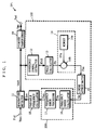
- the OFDM demodulating apparatus DP includes an input terminal Pid, a quadrature detector 11, a phase difference detector 100, a frequency error detector 200, a variable frequency oscillator 18, a Fourier Transformer 19, and an output terminal Pod.
- the input terminal Pid is connected to a receiver of the receiving station (not shown in Fig. 1) for receiving the OFDM signal Vmo1 therefrom.
- the variable frequency oscillator 18 generates an oscillating signal Sov whose frequency is variable.
- the phase error detector 100 includes a reference symbol extractor 12, a phase calculator 13, a memory 14a, a subtracter 14b, a phase difference calculator 14, and a linear approximator 15.
- the frequency error detector 200 includes a frequency error calculator 16 and a frequency error calculator 17.
- the quadrature detector 11 is connected to the input terminal Pid and the variable frequency oscillator 18 for receiving the OFDM signal Vmo1 and the variable oscillating signal Sov, respectively , therefrom.
- the quadrature detector 11 orthogonally detects the OFDM signal Vmo1 based on the variable oscillating signal Sov to generate a complex detection signal Vmd1.
- the reference symbol extractor 12 of the phase error detector is connected to the quadrature detector 11 for receiving the complex detection signal Vmd1 therefrom.
- the reference symbol extractor 12 extracts only reference symbols RS from the complex detection signal Vmd1 based on a symbol synchronization signal internally generated therein, and outputs the extracted symbols RS as an extracted reference symbol data RSd1.
- the phase calculator 13 is connected to the reference symbol extractor 12 for receiving the extracted reference symbol data RSd1 therefrom.
- the phase calculator 13 calculates the phase Ph of each reference symbol RSd1 extracted from the complex detection signal Vmd1 under the following equation (1).
- Ph arctan (Im/Re) wherein Im is a real part, and Re is an imaginary part of the reference symbol RS of the complex data Vmd1.
- the subtracter 14b is provided between the phase calculator 13 and the linear approximator 15 for receiving the phase Ph from the calculator 13, and is connected to the memory 14a for receiving the phase information IPm therefrom.
- the subtracter 14b makes a subtraction of phase IPm of complex data signal Vmf on transmitting side and phase Ph of complex detection signal Vmd1 on receiving side, and obtains the phase error Phe that is difference therebetween.
- the memory 14a and subtracter 14b construct a phase difference calculator 14 connected to the phase error calculator 14 for receiving the calculated phase Ph therefrom to calculate a phase difference Phe between the second complex data Vmf and the complex detection signal Vmd1 in phase.
- the linear approximator 15 is connected to the phase difference calculator 14 for receiving the phase error Phe therefrom.
- the linear approximator 15 approximates the phase difference Phd to a linear characteristics which can be expressed as a direct function of time for suppressing noise components in the phase difference.
- the linear approximator 15 outputs the gradient Ga of such approximated line.
- the frequency error calculator 16 of the frequency error detector 200 is connected to the linear approximator 15 for receiving the gradient Ga therefrom. Based on this gradient Ga, the frequency error calculator 16 calculates a frequency error Fe of the complex detection signal Vmd1.
- the frequency error processor 17 is connected to the frequency error calculator 16 for receiving the frequency error Fe therefrom.
- the frequency error processor 17 applying the frequency error Fe to smooth thereof over plural frames, and generates a smoothed frequency error Fes.
- the variable frequency oscillator 18 is connected to the frequency error processor 17 for receiving the smoothed frequency error Fes therefrom.
- the variable frequency oscillator 18 generates the oscillating signal Sov having frequency variable according to the smoothed frequency error Fes.
- the quadrature detector 11 can detect the OFDM signal Vmo1.
- the complex detection signal Vmd1 is generated by detecting the OFDM signal Vmo1 with respect to the oscillating signal Sov whose frequency error is corrected by the phase error detector 100 and frequency error detector 200 before the Fourier transformation by the Fourier transformer 19. Therefore, the original complex data Vms demodulated from the complex data Vmd1 is secured it's broadband synchronization.
- RSVmo1(t) the reference symbol RSVmo1(t) in the OFDM signal Vmo1 is expressed by the following equation (2).
- RSVmo1(t) RSVmfr(t) ⁇ exp(j ⁇ 2 ⁇ (fc+ ⁇ f) t) + NVmo1(t)
- RSVmfr(t) is a reference symbol RS of the base-band OFDM signal Vmfr
- t time
- j is a complex
- fc a frequency of the oscillating signal Sov output from the variable frequency oscillator 18
- NVmo1(t) is noise occurred in transmission path from the modulating apparatus MC1 to the demodulating apparatus DP1
- ⁇ f is a frequency error caused by the variation of quartz crystal in a tuner of receiver.
- the reference symbol RSVmd1(t) in the complex detection signal Vmd1 is expressed by the following equation (3).
- RSVmd1(t) RSVmfr(t) ⁇ exp(j ⁇ 2 ⁇ ft) + NVmd1(t) wherein NVmd1(t) is noise occurred in a transmission path just after the quadrature detector 11.
- the reference symbol extractor 12 outputs the reference symbol RSVmd1(t) as the extracted reference symbol data RSd1.
- phase ⁇ Vmd1(t) of reference symbol RSVmd1(t) on the receiving side is expressed by the following equation (4).
- ⁇ Vmd1(t) arctan( RSVmd1(t) )
- the phase calculator 13 outputs the reference symbol RSVmd1(t) as the phase data Ph.
- the phase calculator 14 calculates the phase ⁇ Vmd1(t) of the reference symbol RSVmd1(t) utilizing the above equations (3) and (4), as expressed as the following equation (5).
- ⁇ Vmd1(t) ⁇ Vmo1(t) + 2 ⁇ ft + ⁇ NVmd1(t)
- ⁇ Vmo1(t) is a phase of reference symbol RSVmo1 on the transmitting side
- ⁇ NVmd1(t) is a phase component of noise NVmo1(t) .
- ⁇ Vmo1(t) is previously stored in the memory 14a as the phase data IPm.
- the subtracter 14b makes a subtraction of the phases ⁇ Vmo1(t) and ⁇ Vmd1(t) to produce a phase difference ⁇ (t) , and outputs the product as the phase error Phe.
- the linear approximator 15 approximates the phase error Phe to a linear characteristics, as typically expressed by the equation (6), to suppress noise components ⁇ NVmd1(t) . Then the approximator 15 asses the gradient ⁇ of the approximated line by utilizing the least squares method.
- the frequency error calculator 16 obtains the frequency difference ⁇ f utilizing the equation (7), and outputs it as the frequency error Fe.
- the frequency error processor 17 applies any one of the following four different processes (Process 1 to Process 4) to the frequency error Fe to adjust thereof.
- adjusted frequency error Fe is output as the smoothed frequency error Fes.
- the variable frequency oscillator 18 controls the frequency fc of the local oscillating signal Sov, generated by itself, according to the smoothed frequency error signal Fes.
- the local oscillating signal Sov having the correct frequency fc is supplied to the quadrature detector 11.
- the frequency error Fe is determined based on the gradient Ga of line, a direct function of time, approximated to the phase error Phe of reference symbols RS. Therefore, even in the case that the frequency difference ⁇ f is bigger than the sub-carrier interval, the gradient Ga of approximated line simply becomes larger, enabling the correct detection of the frequency error Fe. Thus, the frequency synchronization can be secured in a broadband. Still further, frequency error detection using the reference symbols is always correct regardless of the modulation method of sub-carriers.
- FIG. 3 an OFDM demodulating apparatus according to a second embodiment of the present invention is shown.
- the OFDM demodulating apparatus DP2 in Fig. 3 has a construction similar to that shown in Fig. 1.
- the variable frequency oscillator 18 is replaced by a local frequency oscillator 18a for generating a first local oscillating signal Sov1 having a fixed frequency; and a complex multiplier 18c and a variable frequency oscillator 18b for generating a second local oscillating signal Sov2 having a variable frequency are additionally provided.
- the output of the frequency error detector 200 is connected to the variable frequency oscillator 18b.
- the quadrature detector 11 performs the quadrature detection of the OFDM signal Vmo1 based on the first local oscillating signal Sov1 to produce a complex detection signal Vmd1'.
- the reference symbol extractor 12, phase calculator 13, phase error calculator 14, and linera approximator 15 of the phase error detector 100 produces the reference symbol data RSd1', phase data Ph, phase error data Phe, and gradient data Ga, respectively, in the same manner as in the first embodiment.
- the frequency error calculator 16 of the frequency error detector 200 produces the data Fe.
- the frequency error processor 17 applies either one of the Process 1 and Process 2 to the frequency error Fe and outputs the smoothed frequency error data Fes.
- the variable frequency oscillator 18b controls the frequency of the second local oscillating signal Sov2 with respect to the smoothed frequency error data Fes, and supplies the phase variation vector to the complex multiplier 18c.
- This phase variation vector is a complex vector which can be expressed as a function of exp(j2 ⁇ ft) .
- the complex multiplier 18c applies the complex multiplication of the phase variation vector to the complex detection data Vmd1' to remove the phase variation due to frequency error included therein. As a result, the phase variation corresponding to the frequency error can be removed from the complex detection signal even when the frequency varies so badly in the receiver.
- the OFDM modulating apparatus MP2 has a construction similar to that of the apparatus MP1 in Fig. 10, but a reference complex vector inserting unit 76 and a complex multiplier 77 are additionally inserted between the input terminal Pim and the reference symbol inserting unti 71. Furthermore, the Memory 72 is connected to both the complex multipllier 77 and the reference symbol inserting unit 71 for supplying the reference symbol data Sm thereto.
- the reference complex vector inserting unit 76 inserts a reference complex vector Vrc into the original complex data Vms to produce a reference complex vector inserted data Vmsc. Specifically, the reference complex vector inserting unit 76 assigns plural sub-carriers to the original complex data Vms, and also assigns the reference complex vectors Vrc to predetermined plural sub-carriers.
- the construction of thus produced reference complex vector inserted data Vmsc is shown in Fig. 5, wherein the reference complex vectors Vrc indicated as three upward arrows, for example, each spaced by plural original complex data Vms assigned to sub-carriers indicated as upright lines on the frequency axis f.
- the unit 76 outputs every symbol of thus assigned vector Vmsc to the complex multiplier 77.
- the complex multiplier 77 performs a complex multiplication of the complex data Vmsc by the reference symbol RS (Sm) fed from the memory 72, and outputs the product Vmcc to the reference symbol inserting unit 71.
- the reference symbol inserting unit 71 inserts the reference symbol RS into the modulated complex data Vmcc, in a manner previously described with reference to Figs. 2 and 10, to further produce a modulated complex data vmf'.
- the inverse Fourier transformer 73 and the quadrature modulator 74 also perform the same processes as those in the apparatus MP1 and produces a second base-band data Vmfr' and a second OFDM signal Vmo2, respectively.
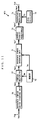
- the OFDM demodulating apparatus DP3 in Fig. 4 has a construction where the apparatus DP1 in Fig. 1 further includes an equalizer 300 connected to the Fourier transformer 19 and a phase compensator 400 connected between the equalizer 300 and the output port Pod.
- the second OFDM signal Vmo2 instead of the first OFDM signal Vmo1 is supplied to the input terminal Pim, and a first reproduced original complex data Vms1 instead of the complex data Vms is output from the output from the Fourier transformer 19 in the demodulating apparatus DP3 according to this embodiment.
- the equalizer 300 includes a reference symbol extractor 30, a memory 31, and a complex divider 32 to produce a equalized reproduced data Vmc.
- the reference symbol extractor 30 extracts reference symbol RSs1 from the first reproduced complex data Vms1 which the memory 31 stores therein.
- the complex multiplier 30 applies a complex division process to all the reproduced data Vms1 from the transformer 19 with the reference symbol RSs1 stored in the memory 31.
- the first reproduce complex data Vms1 is equalized such that components of amplitude phase distortion are removed from the first reproduced complex data Vms1 and such distortion component removed data is output as a transitional reproduced data Vmc. Note that the construction and operation of equalizer 300 are detailedly disclosed in the U.S. Patent No.
- the phase compensator 400 includes a reference vector extractor 20, a phase calculator 21, a memory 22, a phase error calculator 23, a phase error averaging unit 24, a phase converter 25, and a complex multiplier 26.
- the reference complex vector extractor 20 is connected to the complex divider 32 of the equalizer 300 for receiving the transitional reproduced data Vmc.
- the extractor 20 extracts the reference complex data Vrc from the data Vmc to produce an extracted reference complex data signal Vcs indicative of thus extracted reference complex vector Vrc.
- the phase error calculator 21 is connected to the reference complex extractor 20 for receiving the signal Vcs therefrom for calculating the phase of extracted reference complex vector Vrc.
- the memory 22 is provided for previously storing the phase information IPc indicative of the reference complex vector Vrc therein.
- the phase error calculator 23 is connected to the phase calculator 21 and memory 22 for receiving the phase signal Phc and the phase information IPc, respectively, therefrom. Based on these data Phc and IPc, the phase error calculator 23 calculates the phase error Phec which is a difference in frequency between the complex vector Vrc before and after transmission.
- the phase error averaging unit 24 is connected to the phase error calculator 23 for receiving the phase error data Phec therefrom to average the phase difference Phec and obtain an averaged phase difference Phem.
- the phase convertor 25 is connected to the averaging unit 24 for receiving the averaged phase difference Phem to covert the coordinate system of them into a polar coordinate system and to obtain a phase compensation vector Vhei necessary to compensate the phase error Phem.
- the complex multiplier 26 is connected to the complex divider 32 of the equalizer 300 for receiving the transitional reproduced data Vmc therefrom and to the phase convertor 25 for receiving the phase compensation vector Vhei therefrom.
- the complex multiplier 26 performs the complex multiplication of the transitional reproduced data Vmc which is an output from the Fourier transformer 29 and the phase compensation vector Vhei.
- the multiplier 26 compensates the phase error of the reproduced data Vmc by the compensation vector Vhei, and outputs a product as a second reproduced complex data Vmo2.
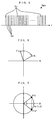
- phase shift of reference complex vector Vrc caused by the residual phase shift is shown.
- the reference complex vector Vrc that should be originally located on a position Pk rotates on the complex plane by the residual shifting amount and moves to a position P'k.
- This movement can be estimated by calculating the phase error Phec with the phase error calculator 23.
- This estimated shift movement Phec is smoothed over plural reference complex vectors by the phase error averaging unit 24.
- the complex vector for reverse-shifting the averaged phase error Phec is calculated by the phase convertor 25. Specifically, the movement amout between Pk and P'k is averaged, reversed, and then converted into a polar coordinate system, obtaining the compensation vector Vhei.
- the complex multiplier 26 performs a complex multiplication of all the reproduced vector Vmc by the phase compensation vector Vhei, and removes the influence of the phase shift.
- the original complex data Vms can be reproduced correctly even if the residual phase shift due to noise suppression by the linear approximation occurs because such phase shift is precisely estimated.
- the reference complex vector Vrc has predetermined value by multiplying the demodulated vector with reference symbol combined with a pseudo random noise signal or frequency sweeping signal, an over-concentration of power to the OFDM signal after the inverse Fourier transformation can be prevented.
- the pseudo random noise signal and the frequency sweeping signal typically including the frequency characteristics on the transmission path. Therefore, application of the pseudo random noise signal or the frequency sweeping signal to the reference symbol enables a precise estimation of transmission path characteristic, and equalization of thereof.
- the OFDM demodulating apparatus DP3 can compensate the phase error (shift) due to the local oscillating signal even if the phase error detector 100 and frequency error detector 200 are removed therefrom, and the variable frequency oscillator 18 is replaced by a local frequency oscillator. Still further, it is also possible to supply the complex detection signal Vmd1 from the complex multiplier 18c of the apparatus DP3 (Fig. 3) to the Fourier transformer 19.
- the OFDM demodulating apparatus DP4 of this example has a construction very similar to that of the apparatus DP3 shown in Fig. 4, but the phase calculator 21, memory 22, phase error calculator 23, phase error averaging unit 24, and the phase covertor 25 therein are replaced with an averaging unit 27, normalizing unit, and complex conjugate calculator 29.
- the reference complex vector inserting unit 75 of the OFDM modulating apparatus MP2 assigns plural sub-carriers to the original complex data Vms, and also assigns the reference complex vectors Vrc (A,0) to predetermined plural sub-carriers according to this embodiment. Note that A is a real number except zero. Then, the unit 76 outputs every symbol of thus assigned vector Vmsc to the complex multiplier 77. Thenafter, the operation of OFDM modulating apparatus MP2 is the same as those previously described with reference to Fig. 8.
- the averaging unit 27 is connected to the reference complex vector extractor 20 for receiving the extracted reference vector Vcs to average thereof and produce the averaged reference complex vector Vcm.
- the normalizing unit 28 is connected to the averaging unit 27 for receiving the averaged vector Vcm to divde the amplitude thereof by A therefrom, and produce a normalized complex vector Vcr.
- the complex conjugate calculator 29 is connected to the normalizing unit 28 for receiving the normalized complex vector Vcr therefrom to obtain a complex conjugate Vcc.
- the complex multiplier 26 is connected to both the complex divider 32 and the complex conjugate calculator 29 for receiving the reproduced vector Vmc and the conjugate Vcc, respectively, therefrom to obtain the complex multiple Vms 3 thereof.
- the demodulated vector Vmc from the complex divider 32 include the residual phase error caused by the noise suppression by the linear approximator 15.
- FIG. 7 the phase shift of reference complex vector Vrc caused by the residual phase shift is shown.
- P k* (Xk, -Yk) which is a complex conjugate of P K to P k.
- This complex conjugate Pk* can be obtained by the following steps.
- the averaging unit 27 smoothes the extracted reference vector Vcs; the normalizing unit 29 adjust the amplitude thereof by dividing with A; the complex conjugate calculator 29 obtains the complex conjugate Vcc; and the complex multiplier 26 applies the complex multiplication to all demodulated vectors to shift back the phase to the original position.
- the phase shift of demodulated vector can be precisely compensated by a simplified construction wherein the phase calculating means 21, 22, 23, 24, and 25 for the apparatus DP3 are not required.
- setting the reference complex vector as (1, 0), the normalizing unit 28 also can be discarded.
- the reference complex vector Vrc has predetermined value (A, 0) by multiplying the demodulated vector with reference symbol combined with a pseudo random noise signal or frequency sweeping signal, an over-concentration of power to the OFDM signal after the inverse Fourier transformation can be prevented.
- the pseudo random noise signal and the frequency sweeping signal typically including the frequency characteristics on the transmission path. Therefore, application of the pseudo random noise signal or the frequency sweeping signal to the reference symbol enables a precise estimation of transmission path characteristic, and equalization of thereof.
- the OFDM demodulating apparatus DP5 of this example has a construction very similar to that of the apparatus DP4 shown in Fig. 8, but the normalizing unit 28 is removed by setting the reference complex vector as (1,0) therefrom.
- every components of the apparatuses MP1, MP2, DP1, DP2, DP3, DP4, and DP5 can be constructed as a physical circuitry as well as software.
Landscapes
- Engineering & Computer Science (AREA)
- Computer Networks & Wireless Communication (AREA)
- Signal Processing (AREA)
- Transmitters (AREA)
- Radio Relay Systems (AREA)
- Digital Transmission Methods That Use Modulated Carrier Waves (AREA)
Applications Claiming Priority (3)
| Application Number | Priority Date | Filing Date | Title |
|---|---|---|---|
| JP3160997 | 1997-02-17 | ||
| JP3160997 | 1997-02-17 | ||
| JP31609/97 | 1997-02-17 |
Publications (2)
| Publication Number | Publication Date |
|---|---|
| EP0859494A2 true EP0859494A2 (fr) | 1998-08-19 |
| EP0859494A3 EP0859494A3 (fr) | 2000-08-23 |
Family
ID=12335953
Family Applications (1)
| Application Number | Title | Priority Date | Filing Date |
|---|---|---|---|
| EP98102595A Withdrawn EP0859494A3 (fr) | 1997-02-17 | 1998-02-16 | Synchronisation de l'oscillateur local, dans des systèmes multiporteurs |
Country Status (1)
| Country | Link |
|---|---|
| EP (1) | EP0859494A3 (fr) |
Cited By (10)
| Publication number | Priority date | Publication date | Assignee | Title |
|---|---|---|---|---|
| EP0987831A1 (fr) * | 1998-09-11 | 2000-03-22 | Motorola, Inc. | Procédé et appareil d'estimation et d'égalisation d'un canal dans un récepteur pour MDFO |
| WO2001020831A1 (fr) * | 1999-09-13 | 2001-03-22 | Matsushita Electric Industrial Co., Ltd. | Dispositif de communication ofdm et procede de detection |
| WO2002028046A3 (fr) * | 2000-09-25 | 2002-07-04 | At & T Wireless Services Inc | Procedes et dispositif permettant de reduire l'erreur de phase residuelle dans des signaux de communication mrof |
| EP1280309A1 (fr) * | 2001-07-27 | 2003-01-29 | Samsung Electronics Co., Ltd. | Récepteur OFDM et procédé correspondant utilisant un système de coordonnées polaires |
| EP1328100A1 (fr) * | 2002-01-09 | 2003-07-16 | Matsushita Electric Industrial Co., Ltd. | Récepteur OFDM (MROF) et procédé pour la correction de phase des signaux reçus par voies multiples en utilisant une séquence d'apprentissage et pour la correction de fréquence et d'horloge en utilisant des symboles pilotes |
| EP1126673A3 (fr) * | 2000-02-16 | 2004-01-07 | Thomson Licensing, Inc. | Correction d'un décalage en fréquence dans un récepteur multiporteuse |
| EP1172956A4 (fr) * | 1999-04-22 | 2006-07-05 | Nippon Telegraph & Telephone | Recepteur de communication par paquets ofdm |
| KR100754721B1 (ko) * | 2002-04-26 | 2007-09-03 | 삼성전자주식회사 | 직교주파수분할다중화 통신시스템에서 다중화 데이터 송수신 장치 및 방법 |
| EP1988676A1 (fr) * | 2007-05-03 | 2008-11-05 | Telefonaktiebolaget LM Ericsson (publ) | Détermination d'une erreur de fréquence dans un récepteur d'un système de communication sans fil |
| CN102129605A (zh) * | 2011-04-06 | 2011-07-20 | 河南工业大学 | 一种基于vmf-nsct的彩色眼底图像降噪新方法 |
Family Cites Families (5)
| Publication number | Priority date | Publication date | Assignee | Title |
|---|---|---|---|---|
| SE501608C2 (sv) * | 1994-01-18 | 1995-03-27 | Telia Ab | Förfarande och arrangemang för synkronisering vid OFDM- modulering |
| SE504787C2 (sv) * | 1994-12-14 | 1997-04-28 | Hd Divine Ab | Metod vid OFDM-mottagning för korrigering av frekvens, tidsfönster, samplingsklocka och långsamma fasvariationer |
| US5682376A (en) * | 1994-12-20 | 1997-10-28 | Matsushita Electric Industrial Co., Ltd. | Method of transmitting orthogonal frequency division multiplex signal, and transmitter and receiver employed therefor |
| JP3145003B2 (ja) * | 1995-03-23 | 2001-03-12 | 株式会社東芝 | 直交周波数分割多重伝送方式とその送信装置および受信装置 |
| EP0735730A3 (fr) * | 1995-03-28 | 1999-07-07 | Matsushita Electric Industrial Co., Ltd. | Dispositif de commande automatique de fréquence |
-
1998
- 1998-02-16 EP EP98102595A patent/EP0859494A3/fr not_active Withdrawn
Cited By (18)
| Publication number | Priority date | Publication date | Assignee | Title |
|---|---|---|---|---|
| EP0987831A1 (fr) * | 1998-09-11 | 2000-03-22 | Motorola, Inc. | Procédé et appareil d'estimation et d'égalisation d'un canal dans un récepteur pour MDFO |
| EP1172956A4 (fr) * | 1999-04-22 | 2006-07-05 | Nippon Telegraph & Telephone | Recepteur de communication par paquets ofdm |
| WO2001020831A1 (fr) * | 1999-09-13 | 2001-03-22 | Matsushita Electric Industrial Co., Ltd. | Dispositif de communication ofdm et procede de detection |
| EP1126673A3 (fr) * | 2000-02-16 | 2004-01-07 | Thomson Licensing, Inc. | Correction d'un décalage en fréquence dans un récepteur multiporteuse |
| CN1293714C (zh) * | 2000-02-16 | 2007-01-03 | 汤姆森特许公司 | 正交频分多路复用系统中的本机振荡器频率校正 |
| KR100758962B1 (ko) * | 2000-02-16 | 2007-09-17 | 톰슨 라이센싱 | 직교 주파수 분할 다중화 시스템에서의 국부 발진기주파수 정정 방법 및 장치 |
| US7548587B2 (en) | 2000-09-25 | 2009-06-16 | At&T Mobility Ii Llc | Methods and apparatus for use in reducing residual phase error in OFDM communication signals |
| WO2002028046A3 (fr) * | 2000-09-25 | 2002-07-04 | At & T Wireless Services Inc | Procedes et dispositif permettant de reduire l'erreur de phase residuelle dans des signaux de communication mrof |
| US6928120B1 (en) | 2000-09-25 | 2005-08-09 | Cingular Wireless Ii, Llc | Methods and apparatus for use in reducing residual phase error in OFDM communication signals |
| US8045634B2 (en) | 2000-09-25 | 2011-10-25 | At&T Mobility Ii Llc | Methods and apparatus for use in reducing residual phase error in OFDM communication signals |
| EP1280309A1 (fr) * | 2001-07-27 | 2003-01-29 | Samsung Electronics Co., Ltd. | Récepteur OFDM et procédé correspondant utilisant un système de coordonnées polaires |
| EP1328100A1 (fr) * | 2002-01-09 | 2003-07-16 | Matsushita Electric Industrial Co., Ltd. | Récepteur OFDM (MROF) et procédé pour la correction de phase des signaux reçus par voies multiples en utilisant une séquence d'apprentissage et pour la correction de fréquence et d'horloge en utilisant des symboles pilotes |
| US7376074B2 (en) | 2002-04-26 | 2008-05-20 | Samsung Electronics Co., Ltd | Apparatus and method for transmitting and receiving side information of a partial transmit sequence in an OFDM communication system |
| KR100754721B1 (ko) * | 2002-04-26 | 2007-09-03 | 삼성전자주식회사 | 직교주파수분할다중화 통신시스템에서 다중화 데이터 송수신 장치 및 방법 |
| EP1988676A1 (fr) * | 2007-05-03 | 2008-11-05 | Telefonaktiebolaget LM Ericsson (publ) | Détermination d'une erreur de fréquence dans un récepteur d'un système de communication sans fil |
| WO2008135541A1 (fr) * | 2007-05-03 | 2008-11-13 | Telefonaktiebolaget Lm Ericsson (Publ) | Détermination d'une erreur de fréquence dans un récepteur d'un système de communication sans fil |
| CN102129605A (zh) * | 2011-04-06 | 2011-07-20 | 河南工业大学 | 一种基于vmf-nsct的彩色眼底图像降噪新方法 |
| CN102129605B (zh) * | 2011-04-06 | 2012-09-05 | 河南工业大学 | 一种基于vmf-nsct的彩色眼底图像降噪新方法 |
Also Published As
| Publication number | Publication date |
|---|---|
| EP0859494A3 (fr) | 2000-08-23 |
Similar Documents
| Publication | Publication Date | Title |
|---|---|---|
| EP0601855B1 (fr) | Egaliseur adaptatif, capable de compenser un décalage de la fréquence porteuse | |
| JP4149044B2 (ja) | ディジタル多重搬送波信号の位相及び/又は周波数誤差を訂正する方法及び回路装置 | |
| JP3079950B2 (ja) | 直交周波数分割多重変調信号の受信装置及び伝送方法 | |
| US5959965A (en) | Digital broadcasting receiver | |
| US5875215A (en) | Carrier synchronizing unit | |
| EP2276212A2 (fr) | Appareil de traitement de signaux, procédé de traitement de signaux et système de réception | |
| JPH07162465A (ja) | 中継装置 | |
| CN102725960B (zh) | 用于相位和振荡器频率估计的方法 | |
| US7187725B2 (en) | Method and apparatus for compensating I/Q imbalance by using variable loop gain in quadrature demodulator | |
| EP0859494A2 (fr) | Synchronisation de l'oscillateur local, dans des systèmes multiporteurs | |
| JPH11112460A (ja) | 直交周波数分割多重信号復調装置 | |
| EP0933903A2 (fr) | Suppression du bruit de phase en réception multiporteur | |
| JP2010050834A (ja) | Ofdmデジタル信号等化装置、等化方法及び中継装置 | |
| JP3794412B2 (ja) | 搬送波再生装置 | |
| CN100449972C (zh) | 正交频分复用信号解调装置 | |
| JPH10290208A (ja) | Ofdm信号伝送システム | |
| JP3342967B2 (ja) | Ofdm同期復調回路 | |
| JP2000165346A (ja) | Ofdm復調装置 | |
| US7649962B2 (en) | Phase error correction circuit | |
| JP4075934B2 (ja) | 搬送波再生装置 | |
| EP1130866B1 (fr) | Correction d'erreurs en quadrature et de gain dans des récepteurs homodynes | |
| US6445752B1 (en) | Apparatus and method for phase tracking in a demodulator | |
| US6947512B1 (en) | Carrier reproducing circuit | |
| KR20040059227A (ko) | 디지털 tv의 위상 오차 추적 장치 및 방법 | |
| JP3892361B2 (ja) | 直交同期検波器、レイク受信器、干渉波キャンセラ、およびインピーダンス測定器 |
Legal Events
| Date | Code | Title | Description |
|---|---|---|---|
| PUAI | Public reference made under article 153(3) epc to a published international application that has entered the european phase |
Free format text: ORIGINAL CODE: 0009012 |
|
| AK | Designated contracting states |
Kind code of ref document: A2 Designated state(s): DE FR GB SE |
|
| AX | Request for extension of the european patent |
Free format text: AL;LT;LV;MK;RO;SI |
|
| PUAL | Search report despatched |
Free format text: ORIGINAL CODE: 0009013 |
|
| AK | Designated contracting states |
Kind code of ref document: A3 Designated state(s): AT BE CH DE DK ES FI FR GB GR IE IT LI LU MC NL PT SE |
|
| AX | Request for extension of the european patent |
Free format text: AL;LT;LV;MK;RO;SI |
|
| 17P | Request for examination filed |
Effective date: 20000913 |
|
| AKX | Designation fees paid |
Free format text: DE FR GB SE |
|
| 17Q | First examination report despatched |
Effective date: 20011010 |
|
| STAA | Information on the status of an ep patent application or granted ep patent |
Free format text: STATUS: THE APPLICATION HAS BEEN WITHDRAWN |
|
| 18W | Application withdrawn |
Withdrawal date: 20020215 |